Your Comprehensive Guide to DIY PCB Creation: From Design to Fabrication
Have you ever wondered how the intricate circuits in your favorite gadgets come to life? The answer often lies in PCBs, and the exciting news is you can create them yourself! DIY PCB (Printed Circuit Board) fabrication empowers hobbyists and professionals alike to bring custom electronic designs to reality. In this guide, we'll demystify the process, exploring various techniques from simple hand-drawn methods to more advanced fabrication, giving you the knowledge and confidence to embark on your own DIY PCB journey.
Understanding the Basics of PCB Design
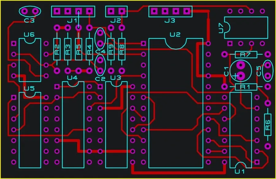
Successful DIY PCB creation hinges on a solid grasp of PCB design fundamentals. This involves understanding the processes of schematic capture, PCB layout, and selecting appropriate software tools. Mastery of these elements ensures a functional and reliable printed circuit board.
- Schematic Capture
The initial stage where electronic circuits are represented using symbols and connections. This involves selecting the right components and ensuring their interconnections accurately reflect the intended circuit function. - PCB Layout
The process of translating the schematic diagram into a physical arrangement of components and traces on the circuit board. Effective layout minimizes signal interference and ensures optimal circuit performance. - Software Tool Selection
Choosing appropriate software is vital for both schematic capture and PCB layout. Tools like KiCad, Eagle, and Altium Designer offer a range of capabilities to suit various needs, from basic designs to complex multi-layer boards. - Key Elements for PCB Design
Crucial design considerations include trace width and spacing, via placement, component footprint, board size and shape, layer count, and consideration of thermal management. These elements directly influence circuit board performance and reliability.
DIY PCB Fabrication Methods: A Detailed Comparison

Creating printed circuit boards (PCBs) at home involves several fabrication techniques, each with its own set of advantages and disadvantages. Choosing the right method depends largely on the desired precision, available resources, and the complexity of the project. This section provides a detailed comparison of the three most popular DIY PCB fabrication methods: toner transfer, photo etching, and CNC milling, to help you decide which is the best for your particular needs.
| Method | Description | Pros | Cons | Recommended Use Cases |
|---|---|---|---|---|
| Toner Transfer | Using a laser printer to transfer a toner mask onto copper clad, then etching the exposed copper. | Low cost, simple process, requires minimal equipment. | Lower resolution, can be unreliable, toner transfer can be inconsistent, less suitable for fine details. | Simple, single-sided boards, for beginners and prototypes, large traces and pads. |
| Photo Etching | Utilizes a photo-sensitive film to create a mask on the copper clad by exposure to UV light and etching. | Higher resolution compared to toner transfer, more reliable results, allows for finer details. | Requires special equipment (UV lamp), higher initial cost, more steps involved, needs careful process control. | Double-sided boards, projects with moderate complexity, needs more precision than toner transfer. |
| CNC Milling | Uses a CNC machine to physically remove copper from the board based on digital design. | High precision, fast fabrication, no chemical etching, complex designs are possible, good for professional-quality PCBs. | Requires expensive CNC milling machine, milling bits wear out, design needs to be tailored to milling process, potential for tool breakage, more complex process to setup. | Complex prototypes, high precision boards, ideal for professional and educational settings, precise trace and pad design. |
Materials and Tools for DIY PCB Projects
Successful DIY PCB fabrication hinges on having the correct materials and tools. This section details the necessary items, categorized for clarity, to ensure you have everything required for your project, from raw board material to precision drilling tools.
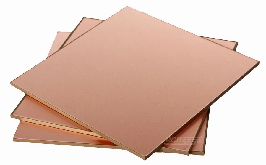
- Raw Materials:
This includes copper-clad boards (single or double-sided, FR4 is common), etchant solution (e.g., ferric chloride or ammonium persulfate), and toner transfer paper or photoresist film. - Design Transfer Tools:
For toner transfer method, you'll need a laser printer, iron, and glossy paper. For photo etching, you need a UV light source, transparent film for the mask and a developer. - Etching Equipment:
Requires a container for etching, safety gloves, eye protection, and materials for agitation or an etching machine. - Drilling Tools:
A drill (hand drill or a drill press) with a set of small drill bits, ideally carbide bits, for creating through-holes and component mounting holes. For precise drilling, a PCB drilling station with a depth gauge is ideal. For larger vias, a step drill bit is useful. - Cutting Tools:
Tools like a PCB shear, rotary tool, or a hacksaw to cut the board to the desired size, a deburring tool, files, or sandpaper to smooth rough edges. - Measurement and Marking Tools:
Ruler, calipers, permanent markers and a fine tip marker are needed for precise measurements and markings for drilling and component placement. - Soldering Equipment:
A soldering iron, solder wire, flux, and desoldering tools like a solder sucker or desoldering wick are necessary for component assembly. - Safety Equipment:
Crucial safety equipment includes safety glasses, chemical-resistant gloves, and adequate ventilation when handling chemicals like etchant solutions.
| Material/Tool | Purpose | Considerations |
|---|---|---|
| Copper-Clad Boards | Base material for the PCB | Choose single or double-sided based on design complexity. FR4 is common due to its balance of performance and cost. |
| Etchant Solution | Removes unwanted copper | Ferric chloride is common but requires proper disposal. Ammonium persulfate is faster but less stable. |
| Laser Printer | Prints the PCB design | Needed for toner transfer. A printer capable of high resolution printing is ideal. |
| UV Exposure Unit | Exposes the photoresist | Needed for photo etching. A homemade UV light box is suitable for many DIY projects. |
| PCB Drill and Drill Bits | Creates holes for components | Carbide bits are preferred for durability. A drill press is preferred over a hand drill for more accuracy. |
| Safety Glasses & Gloves | Personal safety | Essential for handling chemicals and tools. |
Step-by-Step Guide to the Toner Transfer Method
The toner transfer method is a popular and accessible technique for creating DIY PCBs, ideal for beginners due to its low cost and simple equipment requirements. This method involves printing your PCB design onto a specialized transfer paper, then using heat and pressure to transfer the toner to a copper-clad board. Subsequent etching removes the exposed copper, leaving your circuit traces.
- Prepare Your PCB Design
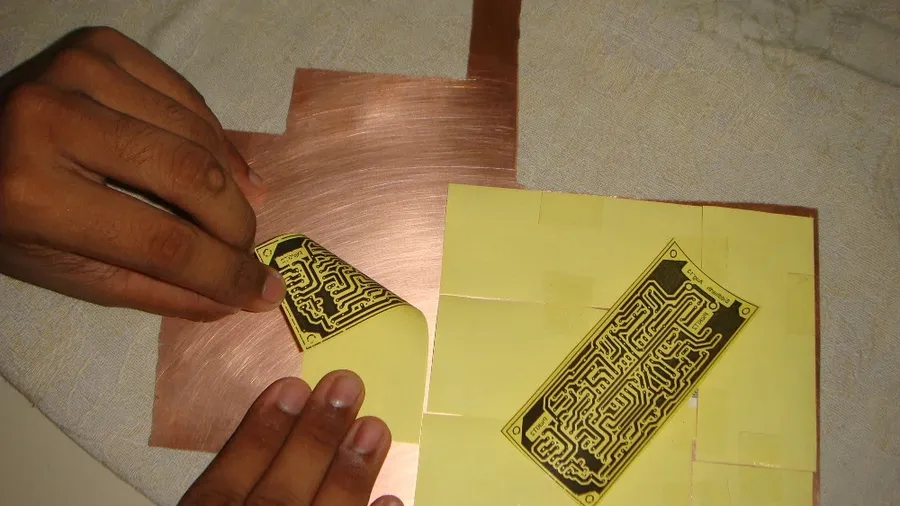
Begin by finalizing your PCB layout using design software like KiCad, Eagle, or Altium. Ensure that your design is mirrored for toner transfer. Print your design onto specialized toner transfer paper or glossy photo paper using a laser printer; ink jet printers will not work for this method. - Prepare the Copper-Clad Board
Clean the copper surface of the board thoroughly. Use fine-grit sandpaper or steel wool to remove any oxidation or contaminants, then wipe it with isopropyl alcohol to ensure good toner adhesion. Avoid touching the cleaned surface with bare hands. - Transfer the Toner
Position the printed transfer paper (toner side down) onto the cleaned copper surface of the board. Secure it in place with heat-resistant tape. Use a household iron set to the highest heat (no steam), apply even pressure across the transfer paper for 5-10 minutes. The board should be placed on a heat resistant flat surface and not a cloth. Avoid movement during transfer. Ensure sufficient pressure to maximize toner adhesion. - Remove the Transfer Paper
After the transfer process, allow the board to cool for a few minutes. Gently submerge the board in warm water and let the paper soften. Carefully peel away the transfer paper to leave the toner adhered to the copper surface. You can use a soft brush or cloth to aid the removal process. If toner is missing, repeat the transfer process with higher heat, greater pressure or a longer transfer time. - Etch the PCB
Prepare an etching solution, such as ferric chloride or ammonium persulfate, according to the manufacturer's instructions. Place the board in the etchant, agitating it periodically. Monitor the etching process closely and remove it once all the exposed copper is dissolved. This process can take 5-20 min depending on the etchant and temperature. Rinse the board thoroughly with water immediately after etching. - Remove the Toner
After the etching is complete, remove the toner by using a solvent such as acetone or paint thinner and a soft cloth or paper towel. Be careful to use in a well ventilated area and not to come into contact with your skin. - Drill Holes
Use a PCB drill press with appropriate drill bits to create the required holes for through-hole components. Use a magnifying lamp for visibility and precision. Clean the drilled PCB before populating with components. A PCB drill is preferable to a hand drill.
| Challenge | Solution |
|---|---|
| Incomplete toner transfer | Ensure sufficient heat, pressure, and transfer time; use appropriate toner transfer paper. |
| Uneven etching | Use fresh etchant, agitate the solution, and monitor the process closely; maintain proper etching solution temperature. |
| Toner lifting during etching | Clean the copper surface thoroughly; ensure good toner adhesion during transfer process; use higher quality toner |
| Difficulty removing transfer paper | Soak the board in warm water; gently rub the paper with a soft brush. |
Mastering the Photo Etching Technique
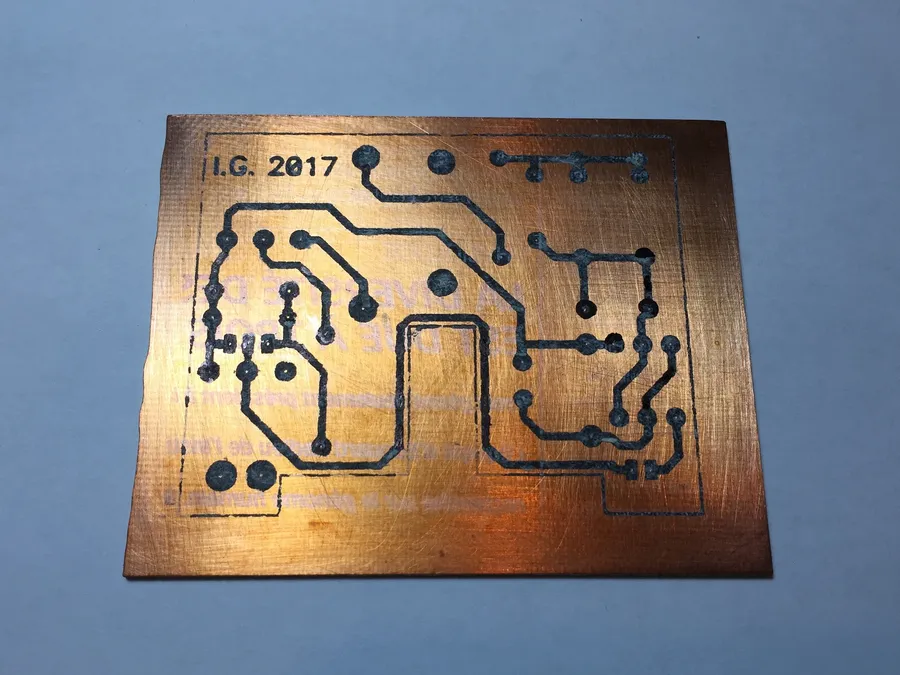
Photo etching offers a precise method for creating DIY PCBs, leveraging light-sensitive materials to transfer intricate designs onto copper-clad boards. This technique involves creating a photo-mask, exposing a photosensitive board to UV light, and then etching away the unwanted copper, resulting in a highly detailed and reliable circuit board.
- Creating the Photo-mask
The photo-mask is a crucial element, typically a transparent film with opaque areas representing the circuit traces and pads. This can be printed on transparency film using a laser printer with high resolution and contrast. Ensuring the mask is completely opaque in the design areas is essential for precise etching. - Preparing the Photosensitive PCB
Photosensitive PCB boards are coated with a light-sensitive resist. The board must be handled carefully in a low-light environment to prevent premature exposure. Clean the board thoroughly to remove any contaminants that might affect the resist adhesion or UV exposure. - Exposing the Board to UV Light
The photo-mask is placed directly onto the photosensitive PCB board and then exposed to a UV light source. The light hardens the resist in the exposed areas, which will later protect the copper from the etching solution. Exposure time is critical; too little will result in incomplete hardening, and too much can cause over-exposure, affecting the design’s integrity. - Developing the Exposed Board
After UV exposure, a developer solution is used to remove the unhardened resist, revealing the copper that needs to be etched. The developing process must be carefully timed to avoid over-developing, which could damage the intended trace patterns. Agitating the board gently in the developer can ensure a uniform result. - Etching the Copper
The board is submerged into an etchant solution, typically ferric chloride. This chemical dissolves the exposed copper, leaving behind the protected traces and pads. The etchant must be kept at the correct temperature, and the solution should be gently agitated to ensure even etching. The etching process needs to be monitored closely to avoid over-etching, which can lead to broken or reduced trace width.
| Step | Description | Key Considerations |
|---|---|---|
| 1. Photo-mask Creation | Print circuit design on transparency film. | High resolution, complete opacity of black areas |
| 2. Board Preparation | Clean and handle photosensitive board carefully. | Avoid direct light, remove contaminants |
| 3. UV Exposure | Expose the board through the photo-mask to UV light. | Accurate exposure time is critical |
| 4. Developing | Remove unhardened resist with a developer solution. | Monitor development time to avoid over-developing. |
| 5. Etching | Submerge in etchant to remove exposed copper. | Maintain correct etchant temperature and monitor process closely |
Advanced Techniques: CNC Milling for PCBs
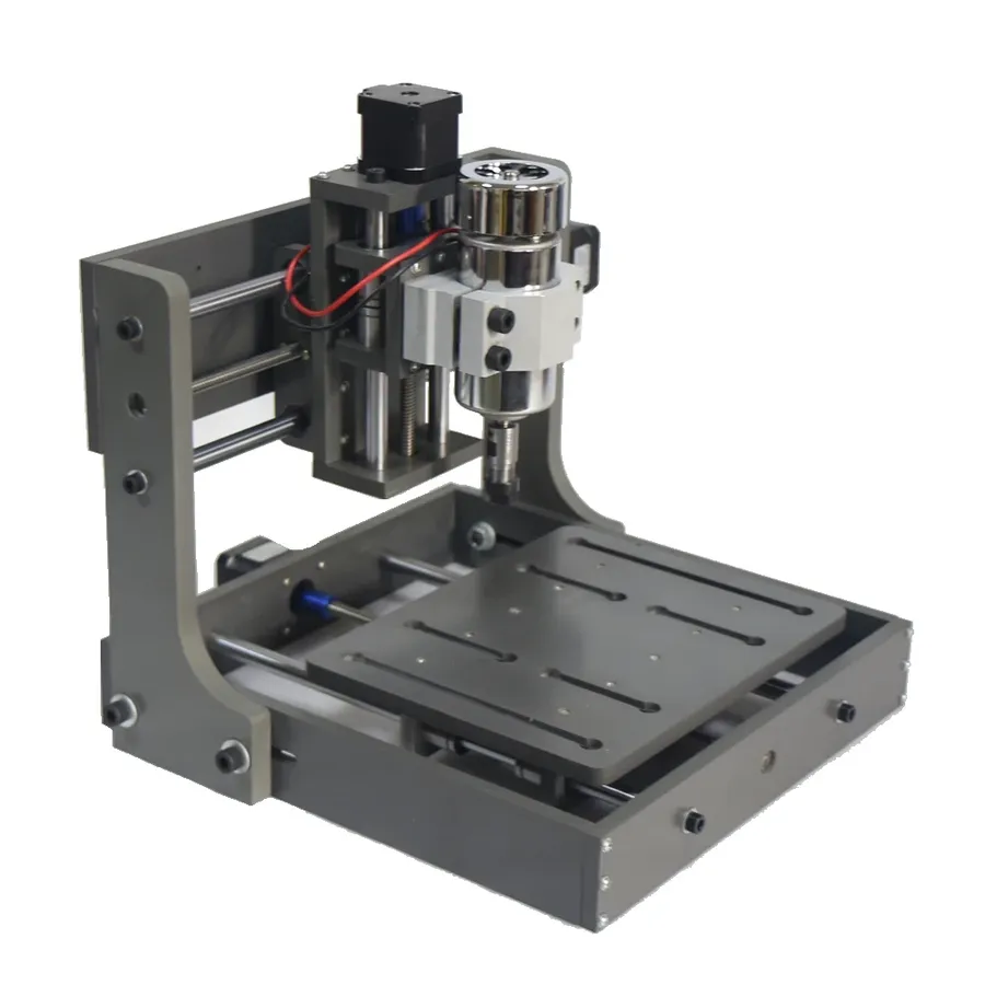
CNC (Computer Numerical Control) milling offers a precise and repeatable method for creating DIY PCBs, moving beyond the limitations of chemical etching or toner transfer. This approach is particularly beneficial for intricate designs and high-precision requirements, allowing for professional-quality results directly from your home workshop.
CNC PCB milling involves using a specialized machine to physically remove copper from a copper-clad board according to the digital design. The process requires careful consideration of several key aspects including machine selection, software for design and control, milling tool selection, and material selection.
- Machine Setup
A CNC milling machine capable of fine movements and accurate positioning is essential. The machine must be stable and properly calibrated. Considerations include spindle speed, step resolution, and the material clamping method. A flat and secure mounting surface is critical for the PCB blank. - Software Integration
The design process for CNC milling starts with PCB design software (like KiCad, Eagle, or Altium). The design is then converted to G-code, which the CNC machine can understand. Software like FlatCAM or similar is used for this conversion and toolpath generation. Careful adjustment of parameters like milling depth and feed rates are needed to ensure the toolpaths are correct. - Milling Tool Selection
The choice of milling tools (end mills, engraving bits) is crucial for achieving quality results. Select the correct tool for the desired cut width and depth; typically smaller diameter tools are better for fine details and track milling, with larger tools for area removal. Always choose tools with a suitable material and geometry for PCB milling. Tungsten carbide tools are recommended due to their hardness and durability. - Best Practices
Before milling, do a 'dry run' to check the path is correct. Start with slow feed rates and speeds, and increase them gradually if the results are good. Properly secure the PCB blank to the machine bed to ensure precision and prevent movement. Use dust extraction to keep the cutting area clear and maintain good visibility. Pay special attention to tool wear and replace tools when necessary.
| Aspect | Considerations |
|---|---|
| Machine Type | Desktop CNC, specific PCB milling machines |
| Design Software | KiCad, Eagle, Altium |
| CAM Software | FlatCAM, or similar to generate G-code |
| Milling Tools | End mills, engraving bits (Tungsten carbide) |
| Milling parameters | Feed rates, spindle speeds, cutting depth |
Essential Design Rules for DIY PCB Success
Successful DIY PCB fabrication hinges on adhering to essential design rules that ensure functionality and reliability. These rules encompass track width, spacing, via sizes, and general layout considerations, which prevent common issues such as short circuits, signal integrity problems, and manufacturing defects. Ignoring these guidelines can lead to non-functional boards and wasted effort; therefore, a meticulous approach to design is crucial.
| Design Rule | Description | Typical Value (for DIY) | Potential Issue if Ignored |
|---|---|---|---|
| Track Width | The width of copper traces carrying electrical signals. | 0.3mm (12 mils) for power, 0.2mm (8 mils) for signal traces. Adjust based on current requirements and copper thickness. | Overheating due to insufficient current capacity; broken traces. |
| Track Spacing | The minimum clearance between copper traces. | 0.2mm (8 mils) minimum. Aim for larger spacing whenever possible. | Short circuits; insulation breakdown leading to shorts. |
| Via Size | Diameter of plated through holes for connecting layers. | 0.8 mm outer diameter, 0.4mm drill diameter. Adjust based on the via's function and equipment capability. | Difficulty in soldering; non-functional layer connections; broken vias due to undersized drill bits or oversized pads. |
| Pad Size | Size of the copper area around component holes to facilitate soldering. | Diameter approximately 1.5 - 2 times of the drill hole; the exact size will also depend on component specification | Difficulty in soldering, solder joints may not hold well; pad lifting. |
| Copper Pour Clearance | The distance between a copper fill and any other copper feature. | 0.2 mm (8 mils) minimum | Short circuits; insulation breakdown leading to shorts. |
| Silkscreen Placement | Positioning of silkscreen for component labels and other markings. | Avoid silkscreen on pads and vias. Maintain at least 0.15 mm clearance from copper features to prevent misprints and interference. | Difficulties in soldering; misidentification of components. |
| Thermal Relief | Connection between copper pours and component pins, especially for power pins. | Use spoke style connections to prevent heat from dissipating too rapidly into the copper pour; typically 4 spokes per pin | Difficulties in soldering power pins; insufficient solder flow and cold solder joints. |
It's crucial to note that these values are guidelines and may require adjustment based on your specific fabrication method and project requirements. For example, toner transfer method has less accuracy than photo etching or CNC milling, therefore, minimum spacing might need to be wider to avoid issues such as shorts. Always check your design against these rules to ensure the best possible outcome.
- Use a PCB design software
Employ design software that automatically checks for rule violations. Software like KiCad, Eagle, or Altium Designer are commonly used. - Start with simple designs
Begin with less complex layouts. Simplify your designs to minimize the risk of error while you are still learning. - Thoroughly review your designs
Review your layout multiple times, checking every trace, via, and pad. Print a 1:1 copy to physically inspect. - Test your PCBs
Before populating the board, test for shorts using a multimeter. Test continuity for signal traces and power rails.
Frequently Asked Questions About DIY PCBs
This section addresses common queries related to DIY PCB creation, providing concise answers and practical guidance for enthusiasts and beginners alike. We aim to clarify the most frequently asked questions, enabling you to confidently embark on your PCB fabrication journey.
- Can I make my own PCB at home?
Yes, it's entirely feasible to make PCBs at home using various methods, including toner transfer, photo etching, and CNC milling. Each method has its own complexity and required tools, but they all allow for the fabrication of custom circuit boards without professional facilities. The suitability of a method depends on the user's skills, budget, and desired precision. - What is the cheapest way to make a PCB?
The toner transfer method is generally the most cost-effective method for DIY PCB fabrication. It requires readily available materials like a laser printer, glossy paper, an iron, and etching chemicals. While it may not offer the highest precision, it is an excellent starting point for hobbyists and is widely accessible due to its low material and equipment costs. Further refinement can be made by using a laminator or specialized transfer paper. - Is it hard to design your own PCB?
PCB design can range from simple to complex, but it is not inherently difficult to learn with modern tools. User-friendly software, tutorials, and online resources make it accessible to beginners. Mastering PCB design does require time and practice, but the basic skills needed to create a simple board are easy to learn. Key concepts include schematic capture, board layout, and following design rules. - Can I print my own PCB?
Yes, using the toner transfer method, you essentially 'print' your PCB design onto a special transfer medium. You can also use other more specialized technologies like direct-write printers, which deposit conductive ink directly onto the substrate but are more expensive. When people refer to 'printing' their PCB, it usually means they are referring to printing the design mask using the toner transfer method. - What are some essential tools I need to get started with DIY PCBs?
Essential tools for DIY PCB fabrication include a laser printer or inkjet printer (for toner transfer or photo etching), copper-clad boards, etching chemicals, a UV light source (for photo etching), drilling tools (for creating holes for components), a laminator or iron (for toner transfer), and a good design software package. A few more useful tools include safety glasses, gloves, and ventilation. - What design software do you recommend for DIY PCB creation?
Several free and open-source design software options are available, such as KiCad, EasyEDA, and Autodesk EAGLE. These platforms provide all necessary tools for schematic capture and PCB layout. The choice of software depends on personal preference, complexity requirements, and experience level, but most of these packages offer robust features and are suitable for both hobbyists and professional use. - How can I ensure that my DIY PCB will work reliably?
Reliability in DIY PCBs depends on adherence to design rules, accuracy in fabrication, and thorough inspection. Following the appropriate trace widths and spacing based on current requirements, correct layer stack up, and checking for shorts or opens are very important. Testing with an appropriate multimeter and visual inspection to verify the fabrication will ensure reliable operation. Attention to detail and careful execution at every stage are crucial to build a reliable PCB.
Troubleshooting Common DIY PCB Issues
Creating DIY PCBs can be a rewarding experience, but it's not without its challenges. This section provides a systematic approach to identifying and resolving the most common issues encountered during the fabrication process, such as etching problems, broken traces, and pad issues.
- Etching Problems
Uneven etching, where some areas of copper are removed more than others, can be due to inconsistent etchant application, contaminated etchant, or uneven temperature. To resolve this, ensure uniform agitation during etching, prepare a fresh batch of etchant, and maintain a consistent temperature throughout the process. Over-etching, where too much copper is removed, can be due to leaving the board in the etchant too long. To avoid this, monitor the process carefully and remove the board once the desired copper is removed. - Broken Traces
Broken or incomplete traces can result from a flawed mask or uneven toner transfer. Inspect the mask carefully for any imperfections before the etching process. For toner transfer, ensure a smooth and even transfer by using a hot laminator and proper pressure. A magnifying glass can be used to inspect for broken traces after etching. If any are found, you can repair them with conductive ink or a thin wire, carefully soldered. - Pad Issues
Issues with pads, like lift-off or incomplete formation, are often due to poor toner transfer, inadequate etching, or improper drilling. Ensure toner is evenly applied by using a quality transfer paper and laminator. Adjust etching times for optimal pad creation, and carefully align your drill bit with the pad centers. Use a center punch to guide the drill bit to avoid pad damage. - Residue on the board after etching
Residue is normally caused by toner resist or excess etchant and it can be removed with a solvent such as acetone and a soft brush. - Short circuits
Short circuits can occur because the copper traces are too close to each other. Verify that the PCB design is correct before printing and use PCB design software to verify the rules and standards. - Drilling problems
Drilling problems can be caused by a dull drill bit or poor drilling technique, it is recommended to use a new drill bit and drill the PCB at low speeds.
DIY PCB fabrication is an empowering skill that allows you to create custom electronic projects at home. From initial design to final fabrication, understanding the various methods and principles will make your DIY PCB projects a success. Whether you start with basic toner transfer or explore advanced CNC milling, the journey of making your own PCBs is sure to be a rewarding one, opening up countless possibilities for innovation and learning in electronics. Always remember to prioritize safety and take your time to learn each step, and you'll be creating your own circuits in no time!