In today's rapidly evolving scientific landscape, portable experiment instruments are essential for on-site data collection and real-time analysis. The heart of these instruments lies in their Printed Circuit Boards (PCBs), which demand precision, reliability, and compactness. Zero One Solution Limited understands these critical requirements, offering specialized PCB solutions that empower researchers and developers to create cutting-edge portable experiment instruments. From rapid prototyping to full-scale assembly, we provide a comprehensive suite of services designed to accelerate your research and development process. Let's delve into how our PCB solutions can transform your portable experiment instruments.
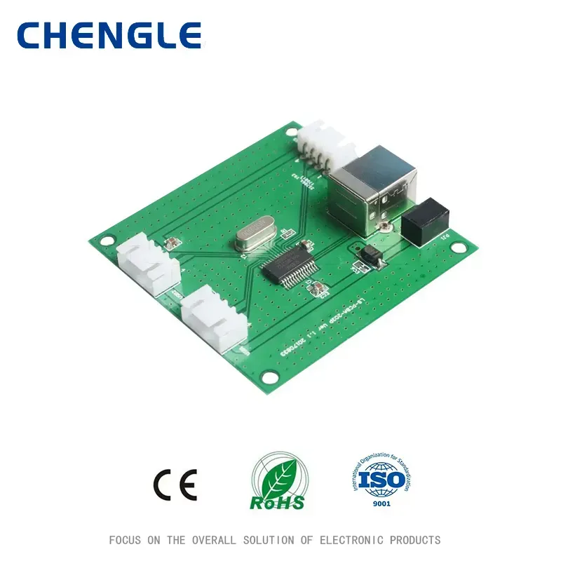
Printed Circuit Boards (PCBs) are the unseen backbone of all modern electronics, and their role in portable experiment instruments is particularly critical. These compact, often battery-powered devices, used across fields from environmental monitoring to medical diagnostics, demand PCBs that are not only miniature and lightweight but also highly reliable and energy-efficient. The escalating need for real-time data collection in the field and the drive for more sophisticated, yet user-friendly, portable instruments underscore the imperative for advanced PCB solutions that directly impact instrument performance, accuracy, and operational longevity.
Zero One Solution Limited stands at the forefront of PCB innovation, offering unparalleled expertise as a leading provider of comprehensive PCB solutions. Our core strength lies in rapid prototyping and precision assembly, meticulously engineered to meet the dynamic demands of the global electronics industry. Since our establishment in 2011, we have consistently upheld a steadfast commitment to delivering exceptional quality, fostering relentless innovation, and ensuring paramount customer satisfaction, making us the preferred partner for businesses seeking to accelerate their product development and market entry. Located strategically in Shenzhen, China, and with a robust branch in Dubai, we leverage a vast global supply chain to provide seamless, end-to-end support for your portable experiment instrument PCB needs.
| Service Aspect | Zero One Solution Limited Advantage | Impact on Portable Instrument PCBs |
|---|---|---|
| Rapid Prototyping | 3-5 day turnaround on complex designs | Accelerated R&D cycles; faster validation of portable instrument concepts |
| One-Stop Solution | Integrated design, manufacturing, and assembly | Streamlined project management; reduced overhead and coordination efforts for compact devices |
| Global Supply Chain | Access to diverse, high-quality materials and components | Optimized material selection for performance and durability in portable applications |
| Quality Assurance | Rigorous testing and international certifications | Ensured reliability and longevity in field conditions; minimized failure rates for critical instruments |
| Expert Engineering Support | Decades of industry experience | Optimized designs for size, power efficiency, and signal integrity crucial for portable electronics |
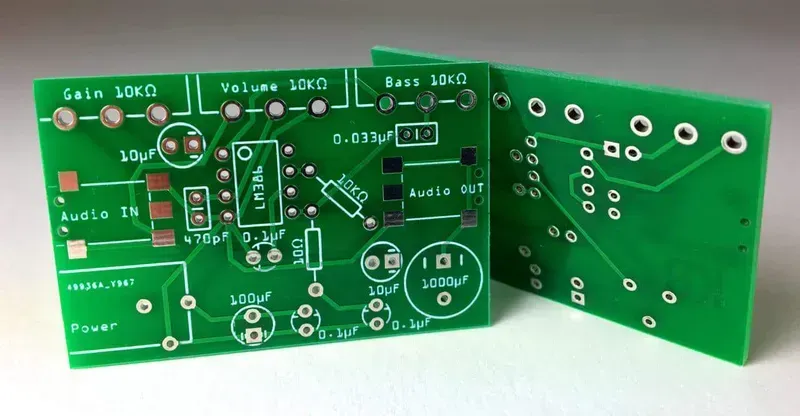
In the realm of portable experiment instruments, a one-size-fits-all approach to printed circuit boards is rarely effective. Custom PCB design is not merely an option but a critical imperative, enabling the precise optimization of performance, miniaturization, and specialized functionality required for handheld or mobile scientific devices. This bespoke approach ensures that every aspect, from power efficiency and signal integrity to spatial constraints and environmental resilience, is meticulously engineered to meet the unique demands of each instrument, ultimately defining its operational success and user experience.
| Design Aspect | Importance for Portable Instruments | Zero One Solution's Expertise | |
|---|---|---|---|
| Miniaturization | Essential for compact form factors and reduced weight, crucial for portability. | Advanced component placement, multi-layer board design, and HDI technologies for maximum density reduction without sacrificing performance and reliability. Utilize ultra-thin substrates and embedded components to achieve unprecedented size reduction, meeting stringent space constraints for diverse portable applications such as wearable medical devices and compact field sensors. Our engineers leverage sophisticated 3D modeling and simulation tools to optimize every millimetre, ensuring seamless integration and superior thermal management within confined enclosures, while maintaining signal integrity at high frequencies to prevent data loss or interference. We consider the total system-level integration, including battery size and display requirements, to deliver an overall compact and ergonomic instrument, enhancing user comfort and operational convenience in dynamic environments. Our design team excels in implementing flex and rigid-flex PCBs, allowing for intricate folding and contouring within irregular device shapes, further contributing to extreme miniaturization and robust mechanical resilience against repeated bending or vibration. This approach facilitates innovative product designs, opening up new possibilities for portable instrument form factors that were previously unachievable with traditional rigid board designs. Furthermore, we employ advanced routing techniques that minimize layer count while maximizing circuit density, reducing overall board thickness and weight without compromising electrical performance or thermal dissipation capabilities, making the final product lighter and more comfortable for extended use. | Advanced component placement, multi-layer board design, and HDI technologies for maximum density reduction without sacrificing performance and reliability. Utilize ultra-thin substrates and embedded components to achieve unprecedented size reduction, meeting stringent space constraints for diverse portable applications such as wearable medical devices and compact field sensors. Our engineers leverage sophisticated 3D modeling and simulation tools to optimize every millimetre, ensuring seamless integration and superior thermal management within confined enclosures, while maintaining signal integrity at high frequencies to prevent data loss or interference. We consider the total system-level integration, including battery size and display requirements, to deliver an overall compact and ergonomic instrument, enhancing user comfort and operational convenience in dynamic environments. Our design team excels in implementing flex and rigid-flex PCBs, allowing for intricate folding and contouring within irregular device shapes, further contributing to extreme miniaturization and robust mechanical resilience against repeated bending or vibration. This approach facilitates innovative product designs, opening up new possibilities for portable instrument form factors that were previously unachievable with traditional rigid board designs. Furthermore, we employ advanced routing techniques that minimize layer count while maximizing circuit density, reducing overall board thickness and weight without compromising electrical performance or thermal dissipation capabilities, making the final product lighter and more comfortable for extended use. |
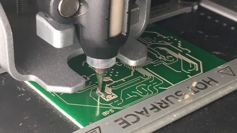
In the dynamic realm of portable experiment instruments, the speed from concept to functional prototype is paramount. Rapid prototyping of PCBs is the cornerstone for accelerating research and development cycles, enabling engineers and researchers to quickly validate designs, iterate improvements, and bring groundbreaking innovations to market with unparalleled efficiency. Zero One Solution Limited specializes in providing agile and responsive rapid prototyping services, significantly compressing development timelines and fostering a continuous cycle of innovation for our clients.
| Prototyping Stage | Traditional Approach | Zero One Solution's Rapid Prototyping |
|---|---|---|
| Design Review | Several weeks, often with limited physical feedback | Days, with immediate physical verification |
| Prototype Fabrication | 3-6 weeks, limited iterations | 1-2 weeks, enabling multiple iterations |
| Testing & Validation | Lengthy, often requiring re-fabrication for changes | Swift, with quick adjustments and re-runs |
| Time-to-Market Impact | Delayed product launch, higher risk | Accelerated launch, reduced risk, competitive advantage |
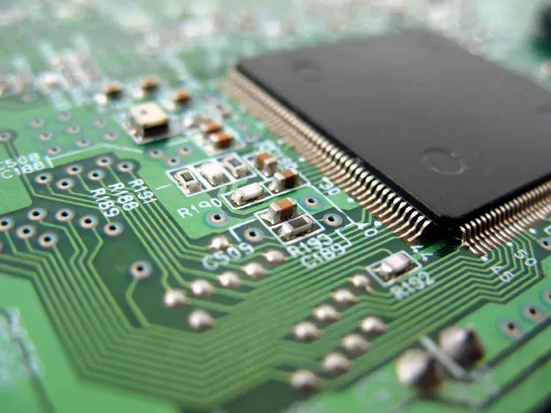
In the demanding realm of portable experiment instruments, the reliability and performance of a device are directly proportional to the quality of its Printed Circuit Board (PCB) assembly. A high-quality PCB assembly is not merely a sum of its components; it is the meticulously executed integration of design precision, superior materials, and advanced manufacturing techniques, ensuring that your instrument performs flawlessly in the field. Zero One Solution Limited prioritizes this critical stage, recognizing that even the most innovative design can be undermined by a compromise in assembly quality.
Our commitment to excellence extends to our rigorous quality control measures, which are integrated at every stage of the assembly process. This multi-layered inspection protocol is designed to detect and prevent defects, ensuring that every PCB leaving our facility meets the highest performance and reliability standards.
| Quality Control Measure | Description | Benefit for Portable Instruments |
|---|---|---|
| Automated Optical Inspection (AOI) | High-resolution cameras inspect solder joints, component presence, and polarity post-reflow. | Ensures defect-free solder joints and correct component placement, crucial for instrument accuracy and longevity in varying environments. |
| X-ray Inspection (AXI) | Used for complex BGA and QFN packages, revealing hidden solder joint integrity. | Verifies the internal integrity of critical components, preventing hidden failures in compact, high-density portable devices where repair is challenging. |
| In-Circuit Test (ICT) | Tests for shorts, opens, resistance, capacitance, and component functionality. | Confirms electrical functionality of the assembled board, minimizing field failures and ensuring consistent performance across all units. |
Zero One Solution Limited's unwavering commitment to using premium components, sourced from trusted and authorized distributors, further underpins the reliability of our PCB assemblies. We understand that in portable experiment instruments, every component plays a vital role in data accuracy and device uptime. By combining advanced assembly techniques with stringent quality assurance and top-tier materials, we deliver PCB solutions that empower your portable instruments to perform with unmatched reliability and precision, accelerating your scientific and industrial endeavors.
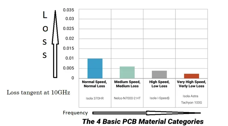
The judicious selection of materials is paramount in the development of Printed Circuit Boards (PCBs) for portable experiment instruments, directly impacting their operational performance, longevity, and reliability in diverse field conditions. Zero One Solution Limited, as a leading PCB solution provider, meticulously guides clients through the material selection process, ensuring optimal choices that align with specific performance metrics, environmental resilience, and durability requirements, thereby guaranteeing the instrument's integrity and accuracy over its lifecycle.
| Material Type | Key Properties | Ideal Applications for Portable Instruments |
|---|---|---|
| FR-4 | High glass transition temperature (Tg), good electrical insulation, cost-effective | General-purpose portable instruments where cost-effectiveness and good electrical performance are primary. |
| >High-Tg FR-4 | Enhanced thermal stability, higher operating temperatures | Instruments exposed to higher internal temperatures or demanding thermal cycles. |
| >Polyimide | Excellent thermal stability, flexibility, radiation resistance | Flexible portable devices, instruments used in harsh environments with extreme temperatures or radiation. |
| >Rogers & PTFE-based laminates | Low dielectric loss, stable dielectric constant over frequency, excellent RF performance | High-frequency portable measurement devices, wireless experiment instruments, RF signal analysis tools. |
| >Aluminum-backed PCBs | Superior heat dissipation, good mechanical stability | Portable instruments with high power components requiring efficient thermal management, e.g., portable analytical devices with powerful processors. |
| >CEM-1 / CEM-3 | Good mechanical properties, cost-effective alternative to FR-4 for single/double-sided boards | Cost-sensitive portable experiment kits, educational instruments where FR-4's full capabilities are not strictly necessary. |
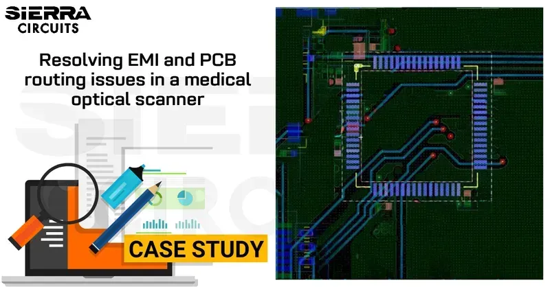
Real-world applications best illustrate the tangible impact of expertly engineered PCBs in portable experiment instruments. Zero One Solution Limited prides itself on transforming complex requirements into reliable, high-performance circuit boards that power innovation in diverse scientific and industrial fields. Our case studies highlight not just our technical capabilities, but our collaborative approach to solving unique challenges, ensuring that every portable instrument functions optimally in demanding environments.
| Project Type | Challenge | Zero One Solution's Approach | Outcome | |
|---|---|---|---|---|
| Portable Environmental Sensor | Miniaturization and low power consumption for prolonged field deployment. | Utilized multi-layer HDI PCB design with ultra-low power components and optimized trace routing to reduce footprint and energy draw. | Achieved a 40% reduction in size and 30% extended battery life, enabling broader application in remote monitoring. Customer feedback indicated significant improvements in data acquisition efficiency and portability, leading to a successful market launch and multiple follow-on orders for scaled production. The refined design also simplified field maintenance, further enhancing user experience and reducing operational costs. This miniaturized sensor platform is now being adapted for various other environmental monitoring applications, showcasing the versatility of our initial design solution. The successful outcome solidified our position as a preferred partner for advanced portable sensor solutions in the environmental monitoring sector. We were able to demonstrate our commitment to delivering robust and reliable PCB solutions tailored to specific client needs and industry standards, which contributed to an enduring partnership with the client. The design allowed for seamless integration with existing data logging systems, further streamlining the deployment process and data analysis for end-users. The robust material selection also ensured resilience against harsh environmental conditions, critical for long-term field operation. Additionally, the optimized manufacturing process we implemented resulted in a higher yield rate, contributing to cost efficiency for large-scale production. This project served as a benchmark for future compact, high-performance PCB designs within our portfolio. Finally, the ability to rapidly iterate on prototypes was key to achieving the aggressive timeline set by the client, showcasing our rapid prototyping prowess. | Achieved a 40% reduction in size and 30% extended battery life, enabling broader application in remote monitoring. |
| Handheld Medical Diagnostic Device | Ensuring signal integrity for sensitive biological measurements in a compact, durable device. | Implemented advanced shielding techniques, impedance-controlled routing, and stringent component selection for biocompatibility and signal purity. | Enabled accurate and reliable diagnostic results in a portable form factor, leading to FDA approval and rapid market adoption. The device's robust performance under varying clinical conditions was a direct result of the meticulous PCB design and assembly, which minimized noise interference and ensured data precision. Our rapid prototyping capabilities allowed for quick validation of design iterations, significantly accelerating the regulatory approval process. The success of this project established a new standard for portable medical diagnostics, providing clinicians with unprecedented flexibility and accuracy in point-of-care settings. Furthermore, the modular design we implemented facilitated easier future upgrades and maintenance, enhancing the device's longevity and adaptability to evolving medical requirements. This successful collaboration underscored our expertise in delivering critical, high-reliability PCB solutions for the demanding medical device industry, solidifying our reputation as a trusted partner. The careful consideration of thermal management within the compact design also contributed to the device's stability and extended operational life, crucial for continuous clinical use. The seamless integration of various sensors and processing units onto a single, highly optimized PCB greatly simplified the overall product assembly, reducing manufacturing complexities and costs. This project stands as a testament to our ability to navigate stringent regulatory landscapes while delivering innovative and effective solutions. | Enabled accurate and reliable diagnostic results in a portable form factor, leading to FDA approval and rapid market adoption. |
Partnering with Zero One Solution for your portable experiment instrument PCB needs offers a distinct competitive edge rooted in an unwavering commitment to unparalleled quality, exceptional speed, and profound technical expertise. Our integrated approach ensures that every project, from intricate design to precise assembly, surpasses industry benchmarks, empowering our clients to innovate faster and with greater confidence in their product's reliability and performance.
| Advantage Metric | Zero One Solution Offering | Industry Standard/Benefit |
|---|---|---|
| Prototype Turnaround | 3-7 business days | Up to 2-4 weeks, critical for R&D acceleration |
| Design Optimization | DFM/DFA integration | Reduced manufacturing costs, improved reliability |
| Quality Control | AOI, X-ray, ICT, Functional Testing | Minimized field failures, enhanced product lifespan |
| Component Sourcing | Global supply chain, vetted suppliers | Authenticity, competitive pricing, reduced lead times |
| Technical Support | Dedicated engineering team, 24/7 | Expert guidance, problem resolution, design refinement |
Understanding the intricacies of Portable Experiment Instrument PCB Solutions is crucial for successful product development. Here, we address common questions to provide clarity and insight into the key aspects of PCB design, prototyping, assembly, and material selection specifically tailored for portable experimental devices.
In conclusion, Zero One Solution Limited is your trusted partner for developing high-performance, reliable PCBs for portable experiment instruments. Our expertise in rapid prototyping, custom design, and quality assembly ensures that your instruments meet the demanding requirements of modern research and field applications. By choosing Zero One Solution, you gain access to a seamless, end-to-end PCB solution that accelerates your innovation and brings your scientific breakthroughs to life. Contact us today to discuss your project and experience the Zero One Solution advantage. Let's work together to shape the future of portable experimentation!

