The intricate dance of electrons within electronic devices owes much to the precision of the drilled PCB. From smartphones to satellites, the foundation of every circuit board relies on accurately placed holes. These seemingly simple perforations are vital for component mounting, signal transmission, and the overall functionality of electronic systems. This article will dive deep into the world of drilled PCB, revealing the processes, challenges, and advancements that underpin modern electronics, connecting the engineering marvel to our daily lives.
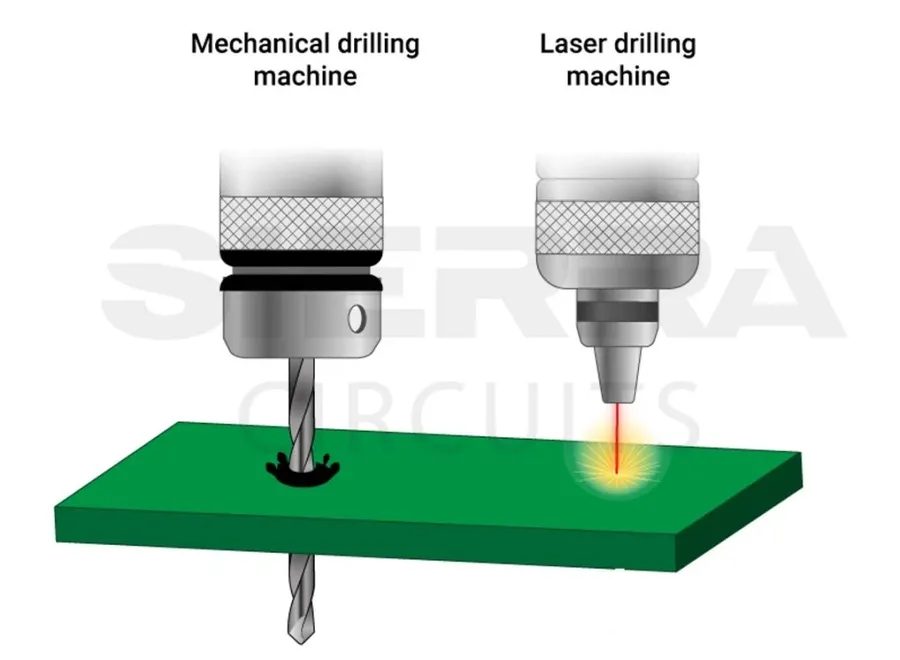
Drilled holes in Printed Circuit Boards (PCBs) are fundamental to their functionality, serving critical roles in component mounting, electrical interconnections, and mechanical stability. The precision of these drilled features is paramount, directly influencing the performance and reliability of the final electronic product. Deviations from specified hole parameters can lead to issues ranging from poor solder joints to catastrophic circuit failures.
Fundamentally, drilled holes on PCBs facilitate the physical insertion and secure attachment of electronic components. Through-hole components, for example, rely on these precisely drilled apertures to establish a stable mechanical interface with the PCB substrate. Moreover, these holes provide the pathways for electrical signals to traverse between different layers of a multi-layered PCB, allowing for complex circuit designs to be realized. In addition to electrical and component mounting functionality, the drilled features also provide mechanical support that is crucial in preventing structural integrity issues with the assembled board.
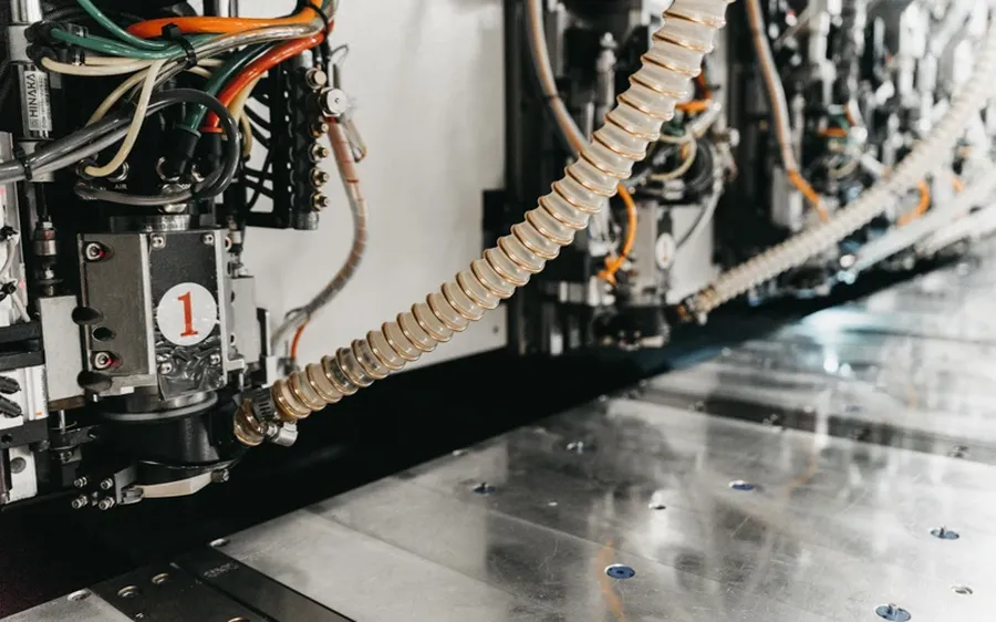
Mechanical drilling is the predominant method for creating holes in printed circuit boards (PCBs), essential for component mounting, electrical connections, and mechanical support. This process involves using precision drill bits, controlled spindle speeds, and accurate depth management to achieve high-quality and consistent hole fabrication. The selection of drill bit types directly influences the quality and precision of the drilled holes, making it a critical factor in PCB manufacturing.
| Drill Bit Type | Material | Application | Advantages | Disadvantages |
|---|---|---|---|---|
| Solid Carbide | Tungsten Carbide | General PCB Drilling | High hardness, good wear resistance, suitable for high-speed drilling. | More expensive than HSS, can be brittle |
| High-Speed Steel (HSS) | Steel Alloy | Less demanding applications, prototype PCBs | Lower cost, more flexible. | Lower hardness, lower wear resistance, not ideal for high-volume production |
| Diamond Coated | Tungsten Carbide with Diamond Coating | Highly abrasive materials, FR-4 | High wear resistance, reduces burrs and rough hole walls | Expensive |
| Cobalt Steel | Steel alloyed with Cobalt | Difficult materials, high heat applications | Heat resistance, suitable for materials that generate high heat during drilling | More expensive than HSS |
The mechanical drilling process involves several key stages. First, the PCB is securely positioned on the drilling machine. A drill bit, chosen based on the material and required hole size, is then mounted on the spindle. The machine then precisely controls the spindle speed and the feed rate as the drill penetrates the board, creating the hole. Accurate depth control is crucial to avoid damaging the underlying layers of the PCB. Post-drilling, the boards are cleaned to remove any debris from the drilling process. This mechanical process allows the creation of highly precise and repeatable holes, ensuring reliable connections and proper component alignment. Drill selection is crucial as it impacts hole wall quality, diameter accuracy, and the overall yield of the drilling process. Proper maintenance and replacement schedules for drill bits are also critical to maintain the necessary precision and quality.
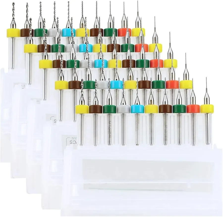
Precision in PCB drilling is governed by several critical parameters, each influencing the final board's functionality and reliability. These parameters include drill size, drilling depth, positional accuracy, and hole diameter tolerance, all of which must be carefully controlled to ensure optimal electrical and mechanical performance. Accurate control over these factors directly impacts the quality and yield of the PCB manufacturing process.
| Parameter | Description | Impact on PCB | Typical Values | Challenges |
|---|---|---|---|---|
| Drill Size | The diameter of the drill bit used to create a hole. | Determines the size of the mounting hole for components, via size, or mechanical attachments. Incorrect size can result in poor component fit or compromised electrical connections. | 0.1 mm to 6.35 mm (0.004" to 0.250"), varies widely based on component needs. | Maintaining the precise drill bit diameter, especially with wear and tear; selecting an appropriate drill bit size based on the pad size of the component. |
| Drill Depth | The depth to which the drill penetrates the PCB material. | Crucial for creating through-holes, blind vias, or back-drilled holes. Improper depth can lead to incomplete connections or damage to underlying layers. | Varies based on PCB layer structure and via type. Controlled by drilling machine settings. | Achieving consistent depth, especially in multi-layer PCBs; managing drill bit wear to ensure consistent hole depth. |
| Positional Accuracy | The precision with which the drill bit is positioned before drilling each hole. Measured by the variance between the planned hole location and the actual location | Affects alignment between different layers of the PCB, as well as the proper positioning of components. Misalignment can result in short circuits, open circuits or component misplacement. | Typically within ±25µm (±0.001"), though can be more precise for advanced boards. Controlled by drill machine and optical registration. | Maintaining precision with high-volume production and tool wear; ensuring accurate registration of each layer in multi-layer PCBs. |
| Hole Diameter Tolerance | The allowed variation in the diameter of the drilled hole from the intended size. | Ensures that components fit correctly, and vias make reliable connections. Too much deviation can cause poor fit or connectivity issues. | Typically ±0.05 mm (±0.002") for through holes, tighter for vias and controlled depth holes. | Controlling hole diameter across different materials and PCB thicknesses; maintaining consistent hole diameter throughout the production run. |
The challenge of small hole drilling is particularly noteworthy. Smaller holes, typically those used for vias, require higher precision and often lead to increased drill bit wear and breakage. Achieving precise hole diameters and positional accuracy becomes increasingly difficult as hole size decreases. In addition, small holes are more susceptible to burrs and wall roughness, which can impact signal integrity.
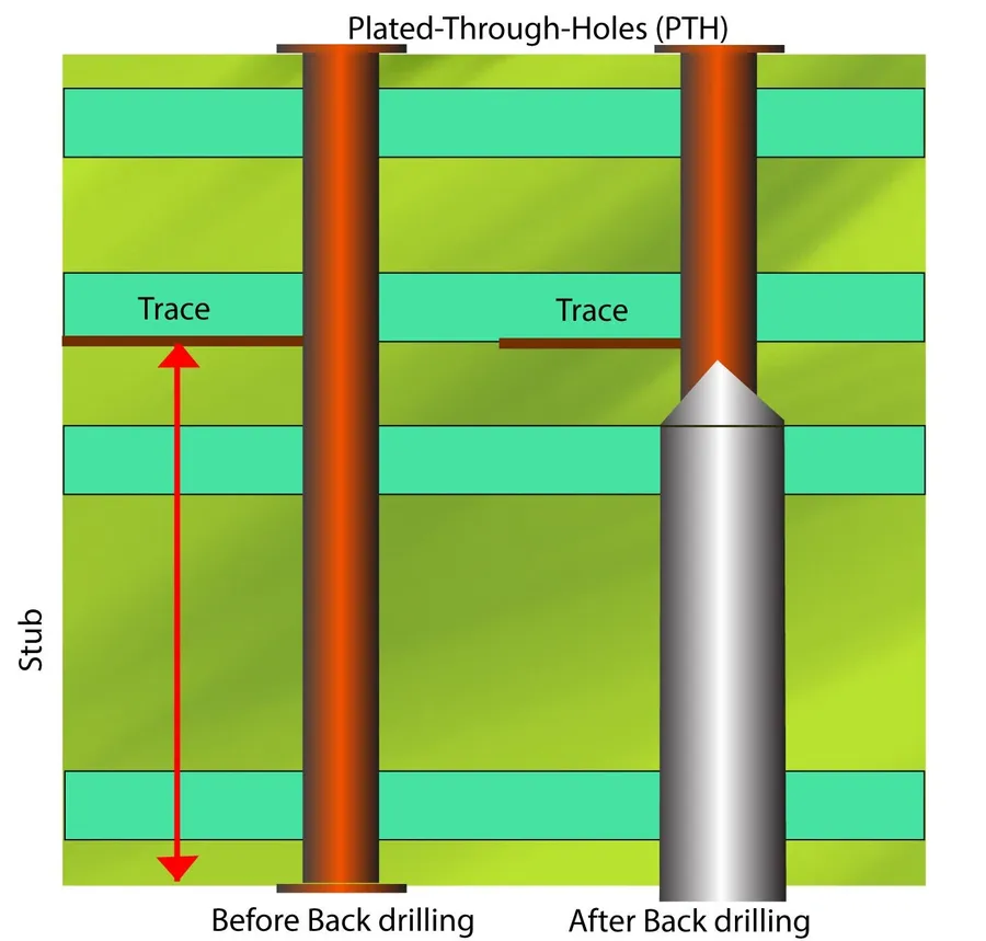
Back drilling, also known as controlled-depth drilling, is a specialized technique used in printed circuit board (PCB) fabrication to remove the unused portion, or 'stub', of a via. This process is critical for improving signal integrity, particularly in high-speed and high-frequency applications, by minimizing signal reflections and distortions that can arise from these stubs.
The back drilling process involves precisely drilling a hole from the back side of the PCB to remove the portion of the via that extends beyond the layer where the signal is being routed. This requires accurate depth control to avoid damaging the active signal layers and ensure the proper connection of the remaining via portion.
Key considerations in back drilling include: drill bit selection, to match the via diameter and material, the drilling depth to precisely remove via stubs, and the process control to maintain positional accuracy and avoid over drilling.
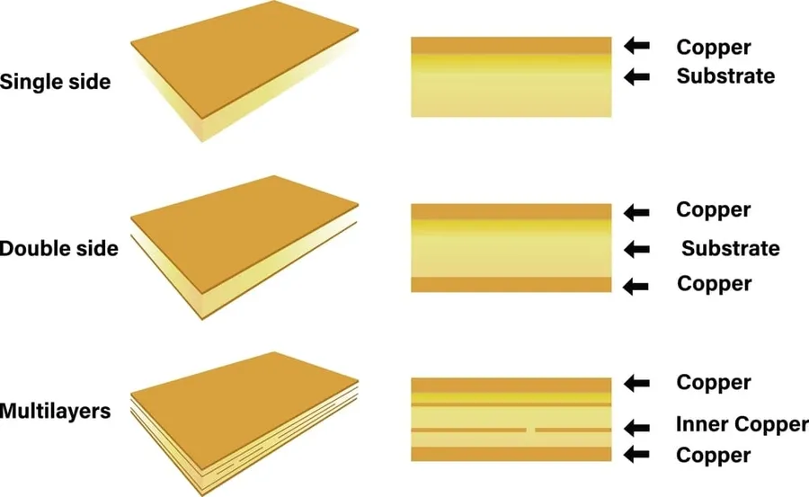
The selection of materials in PCB fabrication significantly dictates the drilling process parameters, tool requirements, and potential issues encountered during production. Different materials exhibit varying mechanical and thermal properties, which necessitate tailored drilling strategies to achieve precise and high-quality hole formation.
| Material Type | Drilling Considerations | Tooling Implications | Common Issues |
|---|---|---|---|
| FR-4 (Fiberglass Epoxy) | Moderate drilling speeds, standard feed rates. Good machinability. | Carbide drill bits are typical. Standard geometry is sufficient. | Fiber pullout, burring |
| High Tg FR-4 | Requires precise control of temperatures due to higher glass transition temperature, Moderate drilling speeds and feed rates. | Carbide drill bits with enhanced wear resistance, optimized geometry. | Increased wear, thermal stress |
| Flexible PCB (e.g., Polyimide) | Lower drilling speeds and feeds are required due to soft material, Precise depth control is crucial. | Specialized drill bits with sharp cutting edges. Micro-drilling tools are common. | Tearing, material deformation |
| Metal Core PCB (MCPCB) | Lower drilling speed, special cooling solutions and high feed rate to reduce the heat generation during drilling is important. | Diamond coated drills, or specialized drills | Tool wear, hole quality issues due to harder material. |
| Teflon/PTFE | Careful management of drilling speed and feed rates because of its soft nature | Specialized sharp carbide drill bits to prevent material build up | Hole deformation, material tear-out |
The drilling process is influenced by the specific material properties. For example, harder materials like FR-4 require robust tools and optimized speeds and feeds to prevent premature tool wear. Conversely, softer materials like flexible polyimide require slower speeds and specific drill geometries to avoid tearing and deformation. Selecting the appropriate drill bit type, such as carbide for standard materials or diamond-coated for abrasive materials, is essential to maintaining hole quality and preventing damage to the PCB.
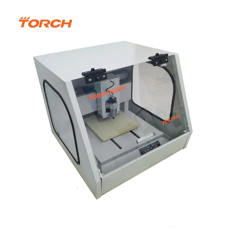
Achieving high precision in PCB drilling is paramount for functionality and reliability; however, the process is fraught with challenges. These challenges encompass issues from the physical integrity of the drilling tools to the accuracy of the drilled holes, each potentially impacting the performance of the final electronic product.
These challenges can have significant impacts on the functionality of the PCB.
To mitigate these challenges, various solutions are implemented in PCB manufacturing:
This section addresses common inquiries regarding drilled PCBs, offering clarity on various aspects from hole types to drilling impacts on design and performance. These insights will assist in understanding the critical role drilling plays in PCB fabrication.
The evolution of drilled PCB technology is being shaped by the increasing demand for miniaturization, higher performance, and improved manufacturing efficiency. Emerging trends are focused on enhancing drilling precision, speed, and cost-effectiveness, leading to advanced techniques and automation that will be pivotal in the future of electronics manufacturing.
The precision of drilled PCB is an unseen but vital aspect of modern technology. From the initial drilling to advanced techniques like back drilling, every step significantly impacts the performance and reliability of electronic devices. As technology continues to evolve, so will the methods used to create these essential components. The continued advancement of drilled PCB technologies guarantees more efficient, reliable and advanced electronic products.

