In today's rapidly evolving technological landscape, remote experimentation has become an indispensable tool for education, research, and development. The core of any successful remote experiment platform lies in its robust and reliable Printed Circuit Board (PCB) design. Zero One Solution Limited, a leading provider of rapid prototyping PCB solutions, offers comprehensive services to meet the unique demands of remote experimentation. With our expertise in PCB design, manufacturing, and assembly, we empower innovators to push the boundaries of scientific exploration from anywhere in the world. Imagine a world where students can conduct complex experiments from their homes, researchers can collaborate across continents, and engineers can test prototypes without the constraints of physical location. The key to unlocking this potential? High-quality, dependable PCB solutions tailored for remote experiment platforms. This article delves into the critical aspects of PCB design for remote experimentation, highlighting Zero One Solution's capabilities and commitment to delivering cutting-edge solutions.
Introduction: The Rise of Remote Experimentation
The paradigm of scientific inquiry and technological development is undergoing a profound transformation, driven by the escalating adoption of remote experimentation platforms. This shift is not merely a convenience but a necessity, enabling researchers, engineers, and educators to conduct complex tests, analyze data, and iterate designs from virtually anywhere in the world. The democratization of access to specialized equipment, often geographically dispersed or prohibitively expensive for individual institutions, underscores the critical evolution towards digitized and networked research environments. This globalized approach to experimentation necessitates robust and reliable hardware foundations, particularly in the realm of Printed Circuit Board (PCB) solutions, which serve as the central nervous system for these sophisticated remote systems.
Why is remote experimentation gaining traction? Remote experimentation offers unparalleled accessibility, cost-efficiency by reducing travel and on-site setup, enhanced collaboration opportunities across global teams, and the ability to conduct experiments in hazardous or inaccessible environments. It democratizes scientific inquiry and accelerates innovation cycles.
What sectors are most impacted by this rise? While initially prominent in academia and research institutions for disciplines like physics, chemistry, and engineering, remote experimentation is rapidly expanding into industrial R&D, product testing, quality control, and even K-12 and higher education, enabling hands-on learning remotely.
What are the primary challenges in implementing remote experiment platforms? Key challenges include ensuring data integrity and security, managing latency and connectivity issues, developing intuitive user interfaces, and critically, designing and manufacturing highly reliable and precise hardware components, particularly PCBs, to ensure accurate and repeatable results.
The Critical Role of PCBs in Remote Experiment Platforms
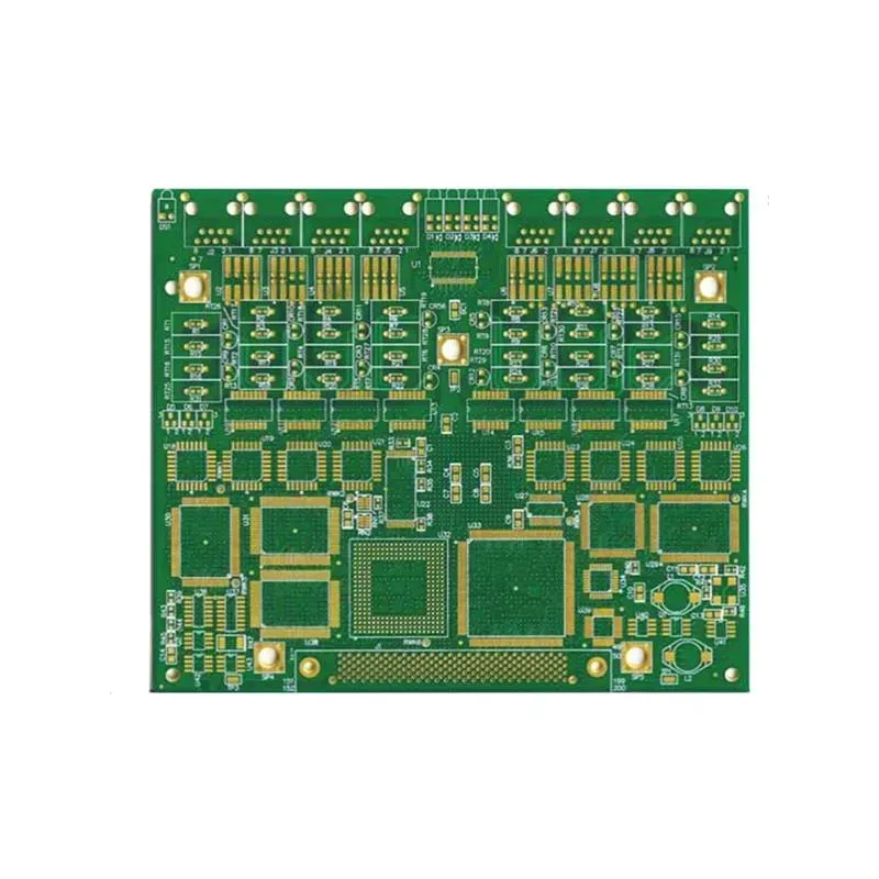
High-Quality PCB Board
The Printed Circuit Board (PCB) serves as the foundational nervous system for any remote experiment platform, dictating its performance, reliability, and ultimately, the integrity of experimental data. In environments where physical presence is impossible or impractical, the robust and precise functionality of the underlying electronics, primarily enabled by high-quality PCBs, becomes paramount. This criticality stems from the need for unwavering signal integrity, efficient power delivery, and resilient thermal management, all of which directly impact the accuracy, stability, and safety of remote experimentation.
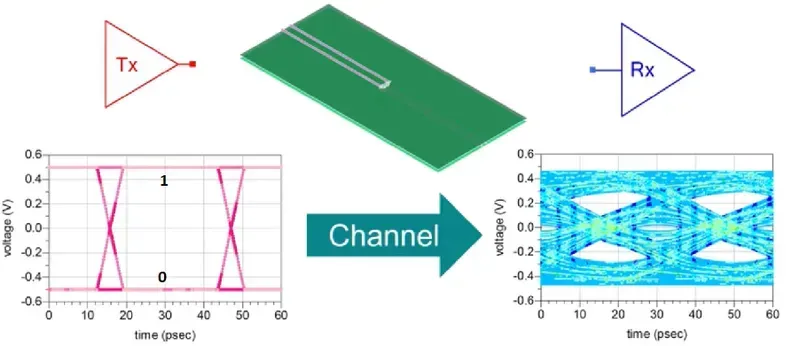
Why is signal integrity so important for Remote Experiment Platform PCBs? Signal integrity is crucial because remote experiments often involve precise measurements and data transmission over distances. Poor signal integrity can lead to data loss, noise interference, and inaccurate readings, compromising the validity of experimental results. High-quality PCB design minimizes impedance mismatches, crosstalk, and electromagnetic interference (EMI), ensuring that signals are transmitted cleanly and accurately from sensors to processing units and communication modules.
How does PCB design contribute to the stability of remote experiments? Stability in remote experiments hinges on consistent and reliable electronic performance, which is a direct outcome of superior PCB design. A well-designed PCB ensures stable power distribution, preventing voltage fluctuations that can lead to erroneous data or component failure. Furthermore, robust physical layout and component placement reduce susceptibility to vibrations and environmental stressors, maintaining operational integrity over extended periods without direct intervention.
What role does PCB quality play in ensuring the safety of Remote Experiment Platforms? Safety is a non-negotiable aspect, particularly in remote or hazardous experimental settings. High-quality PCBs incorporate proper insulation, creepage, and clearance distances to prevent short circuits, arcing, and electrical hazards. Effective thermal management via PCB design prevents overheating of components, mitigating risks of fire or damage to sensitive equipment, thus safeguarding both the experiment and the surrounding environment from potential catastrophic failures.
Are there specific PCB material considerations for remote experiment platforms? Yes, material selection is critical. For remote experiment platforms, materials with stable dielectric properties, good thermal conductivity, and high reliability under varying environmental conditions are preferred. For instance, FR-4 is common, but for high-frequency or high-temperature applications, specialized laminates like Rogers or polyimide-based materials might be necessary to maintain performance and longevity, directly impacting the platform's accuracy and stability.
How does miniaturization impact PCB design for remote experimentation? Miniaturization is a significant trend in remote experimentation, requiring highly compact and integrated PCB designs. This often involves using high-density interconnect (HDI) technology, multi-layer boards, and advanced packaging techniques. While beneficial for space and weight, it intensifies challenges related to thermal dissipation, signal integrity, and manufacturing precision, demanding expert design and fabrication to maintain performance and reliability.
Key Considerations for Remote Experiment Platform PCB Design
PCB Signal Integrity Testing
Designing Printed Circuit Boards (PCBs) for remote experiment platforms demands meticulous attention to specific engineering principles to ensure accurate data acquisition, stable operation, and long-term reliability. Unlike general-purpose PCBs, those for remote experiments must mitigate unique challenges such as signal degradation over long distances, precise power delivery in varied environments, and effective heat dissipation to maintain performance, making these considerations paramount for success.
Signal Integrity (SI) Management Maintaining signal integrity is critical for accurate data transmission in remote experimental setups. This involves careful impedance matching, minimizing crosstalk between traces, and employing proper grounding techniques. High-frequency signals are particularly susceptible to degradation, necessitating advanced PCB layout strategies like controlled impedance routing and differential pair routing to preserve signal quality and prevent data corruption over extended periods or distances. Simulation tools are essential to predict and mitigate SI issues before manufacturing.
Robust Power Distribution Network (PDN) A stable and efficient power distribution network is vital for consistent operation of sensitive instrumentation in remote platforms. The PDN must be designed to minimize voltage drops and ripple, especially in environments where power sources might be unstable or limited. This includes optimizing power plane and trace widths, selecting appropriate decoupling capacitors, and considering the use of power management ICs to regulate voltage and current. Effective PDN design ensures reliable power delivery to all components, preventing operational inconsistencies and measurement errors.
Thermal Management Strategies Heat dissipation is a significant challenge in compact, often enclosed, remote experiment platforms. Components like microcontrollers, FPGAs, and power regulators generate heat, and if not properly managed, can lead to reduced component lifespan, performance degradation, or even catastrophic failure. Effective thermal management involves strategic component placement to facilitate airflow, utilizing thermal vias, integrating heat sinks, and incorporating copper pours on PCBs to act as thermal planes. Passive and active cooling solutions must be considered based on the power density and operational environment of the platform.
Design Aspect
Key Considerations
Impact on Remote Experiment Performance
Component Selection
Industrial-grade components, extended temperature ranges, low power consumption
Ensures reliability in harsh environments, reduces operational costs
Minimizes interference from external sources, prevents data corruption
Mechanical Robustness
Board thickness, material selection, mounting provisions, vibration resistance
Withstands physical stresses during transport and operation, ensures longevity
Connectivity & Interfaces
Standardized connectors, robust headers, secure data links (wired/wireless)
Facilitates seamless integration with sensors and actuators, enables reliable communication
Zero One Solution's Expertise in PCB Solutions
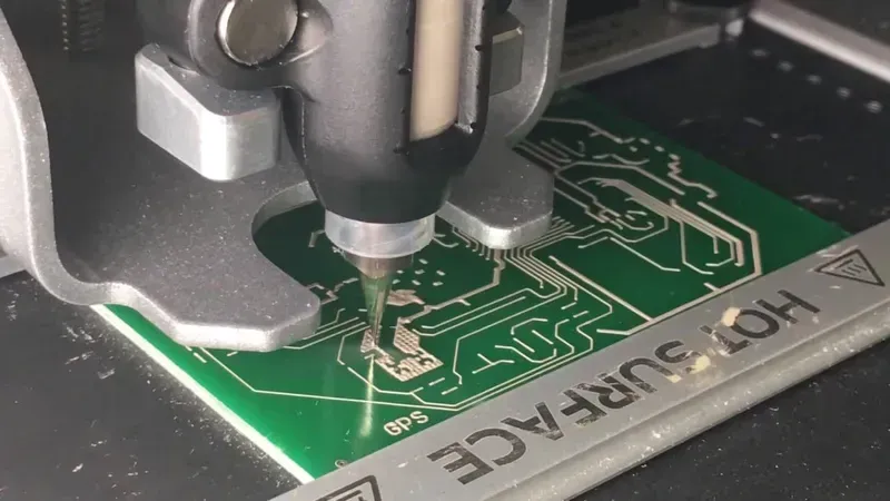
PCB Rapid Prototyping
Zero One Solution Limited stands at the forefront of PCB technology, offering unparalleled expertise in delivering robust and reliable PCB solutions critical for the demanding requirements of remote experiment platforms. Our commitment to precision engineering, accelerated development cycles, and comprehensive quality assurance ensures that every PCB we produce is optimized for the intricate needs of cutting-edge research and development. We empower innovators to transform concepts into tangible, high-performance realities, ensuring seamless data acquisition, stable operation, and system integrity in remote environments.
Rapid Prototyping Excellence Our specialized rapid prototyping services enable clients to swiftly iterate and validate designs. Leveraging advanced equipment and agile methodologies, we compress development timelines from weeks to days, significantly accelerating the market entry of your remote experiment platform innovations without compromising quality or performance. This speed is crucial for meeting the dynamic demands of R&D cycles and maintaining a competitive edge in fast-evolving sectors like IoT, biomedical, and industrial automation, where remote experimentation is paramount.
Our Comprehensive PCB Design Process
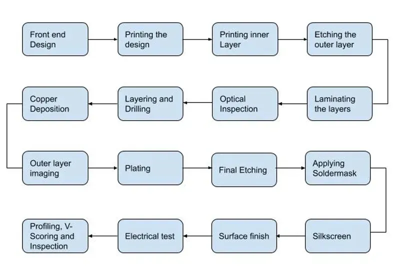
PCB Design Process
Zero One Solution Limited's comprehensive PCB design process is meticulously structured to transform complex concepts into high-performance, reliable remote experiment platform solutions. Our iterative approach prioritizes precision, efficiency, and seamless collaboration, ensuring that every design meets stringent technical specifications and exceeds client expectations from initial consultation through final product delivery.
Phase 1: Initial Consultation and Requirements Analysis We begin with an in-depth consultation to thoroughly understand your remote experiment platform's functional requirements, environmental conditions, performance targets, and budget constraints. This crucial phase involves detailed discussions to capture every nuance of your project, including power delivery, signal integrity, thermal management, and mechanical integration needs. Our experienced engineers translate these requirements into a comprehensive design specification, serving as the blueprint for subsequent stages. This ensures alignment and clarity from the outset, minimizing revisions and accelerating the development cycle. For instance, in a recent project for a high-frequency remote sensor, we identified specific impedance control requirements during this phase, which were critical for data accuracy over long distances, preventing potential signal degradation that could compromise experimental results. This proactive identification is a hallmark of our design process, leading to robust and predictable outcomes. According to IEEE standards, proper impedance matching is paramount for high-speed digital and analog signals, directly impacting the reliability of data transmission in remote systems. Our adherence to such industry best practices is integrated from this foundational stage, ensuring the integrity of the entire PCB solution.
To further illustrate our structured approach, consider the subsequent phases:
Phase 2: Schematic Design and Component Selection Leveraging the detailed specifications, our engineers develop a robust schematic, meticulously selecting components that balance performance, cost, and availability. We prioritize components with proven reliability and adherence to industry standards, ensuring longevity and stability for your remote platform. Our extensive database of qualified components, coupled with real-time supply chain insights, mitigates risks associated with obsolescence and lead times. For example, in designing a remote agricultural monitoring system, we carefully selected low-power, wide-temperature-range components to ensure operation in harsh outdoor environments, extending the system's operational lifespan and reducing maintenance needs. This proactive selection process is supported by our deep understanding of various industry applications and component characteristics. Our strategic partnerships with leading component manufacturers further enhance our ability to source optimal parts, ensuring that the selected components not only meet technical specifications but also contribute to the overall cost-effectiveness and manufacturability of the PCB.
Phase 3: PCB Layout and Routing This phase is where the schematic comes to life. Our layout specialists, employing advanced EDA tools, meticulously arrange components and route traces, strictly adhering to design rules for signal integrity, power distribution, thermal dissipation, and manufacturability (DFM). We employ techniques like differential pair routing, ground plane optimization, and via stitching to ensure signal purity and minimize electromagnetic interference (EMI/EMC), crucial for reliable remote operation. For instance, in a medical remote diagnostic device, our layout engineers implemented precise trace impedance control and isolation techniques to prevent crosstalk and ensure accurate data transmission from sensitive sensors, critical for patient safety and diagnostic reliability. Our proficiency in intricate multi-layer designs allows us to optimize board space while maintaining peak performance, a vital consideration for compact remote experiment modules. This rigorous approach to layout is informed by decades of experience in high-density interconnect (HDI) and high-speed design, ensuring the physical layout translates directly into predictable electrical performance.
Phase 4: Prototyping and Testing Following layout, we proceed with rapid prototyping, leveraging our in-house manufacturing capabilities to quickly produce initial board iterations. These prototypes undergo rigorous testing, including functional testing, signal integrity analysis, power integrity validation, and environmental stress testing. This iterative testing phase identifies and rectifies any potential issues early in the development cycle, preventing costly delays down the line. For example, a remote industrial control unit prototype underwent extensive vibration and temperature cycling tests to simulate real-world harsh environments, ensuring its robustness and operational integrity before mass production. Our testing protocols are aligned with IPC standards, guaranteeing that the manufactured PCBs meet global quality benchmarks. This commitment to thorough validation ensures that the final product is not only functional but also exceptionally reliable under specified operating conditions, providing peace of mind for our clients.
Phase 5: Manufacturing and Assembly Upon successful prototype validation, the design transitions to full-scale manufacturing and assembly. Zero One Solution offers comprehensive DFM (Design for Manufacturability) and DFA (Design for Assembly) analysis throughout the design process to optimize for production efficiency and cost-effectiveness. Our state-of-the-art facilities in Shenzhen and a robust global supply chain ensure high-quality production, whether for low-volume R&D prototypes or high-volume production runs. We employ advanced assembly techniques, including SMT and through-hole, coupled with stringent quality control measures like automated optical inspection (AOI) and X-ray inspection, to ensure every board meets the highest quality standards. This final phase benefits from our integrated one-stop service model, from bare board fabrication to final assembly and testing, providing clients with a seamless and reliable pathway to product realization.
Benefits of Choosing Zero One Solution for Your PCB Needs
Partnering with Zero One Solution for your Remote Experiment Platform PCB Solution provides a distinct competitive edge, leveraging our decade-plus expertise in rapid prototyping and comprehensive PCB services to accelerate your innovation cycle. We empower you with not just components, but a strategic alliance that translates into tangible benefits, ensuring your remote experimentation initiatives are built on a foundation of reliability, efficiency, and cost-effectiveness.
Unrivaled Rapid Turnaround Times Our specialized focus on rapid-response R&D prototype manufacturing means your designs move from concept to physical prototype with unparalleled speed. This agility is critical for iterative development in remote experiment platforms, allowing for faster validation and reduced time-to-market. Our optimized workflows and advanced manufacturing capabilities in Shenzhen minimize delays, transforming your innovative ideas into functional hardware within tight deadlines, giving you a significant first-mover advantage in a competitive landscape.
Cost-Effectiveness Without Compromise Zero One Solution Limited's strategic global supply chain network, headquartered in Shenzhen and with a branch in Dubai, allows us to source high-quality components and materials at competitive prices. This translates into cost-effective PCB solutions for your remote experiment platforms, without ever sacrificing quality or performance. We optimize material utilization and streamline production processes, ensuring you receive the best value for your investment, making advanced experimentation more accessible and economically viable.
Exceptional Customer Support and Collaborative Partnership Beyond manufacturing, Zero One Solution prides itself on fostering a collaborative relationship with our clients. Our dedicated team of veteran engineers provides responsive and insightful customer support from initial consultation through to post-delivery. We act as an extension of your R&D team, offering expert guidance, design-for-manufacturability (DFM) feedback, and proactive communication to address any challenges. This commitment to partnership ensures a seamless and successful journey for your Remote Experiment Platform PCB Solution.
Case Studies: Successful Remote Experiment Platform Projects
Remote Experiment Platform
At Zero One Solution Limited, our commitment to pioneering high-reliability PCB solutions has directly empowered the realization of complex remote experimentation platforms across diverse sectors. These case studies underscore our expertise in translating intricate design requirements into robust, functional PCBs, accelerating innovation and delivering tangible scientific and industrial advancements.
Project Focus
Industry
PCB Solution Provided
Key Outcome
Remote Medical Diagnostics
Healthcare
High-density, low-power, EMI-shielded PCB for sensor integration
Enabled real-time, accurate patient monitoring from remote locations, enhancing diagnostic capabilities and patient care accessibility with minimal signal noise and robust data transmission.
Project Focus
Industry
PCB Solution Provided
Key Outcome
Environmental Sensor Network
Environmental Monitoring
Ruggedized, low-power consumption PCB with integrated wireless communication modules
Facilitated long-term deployment of autonomous environmental sensors in harsh conditions, providing reliable data collection for climate research and pollution tracking over extended periods without frequent maintenance.
Project Focus
Industry
PCB Solution Provided
Key Outcome
Industrial Robotics Control
Manufacturing Automation
Multi-layer, high-current capacity PCB with optimized thermal management and high-speed data interfaces
Supported precise and stable control of robotic arms in remote manufacturing facilities, improving operational efficiency and reducing human exposure to hazardous environments through reliable power delivery and rapid command execution.
Project Focus
Industry
PCB Solution Provided
Key Outcome
Academic Research Lab Automation
Education/Research
Modular, reconfigurable PCB arrays for diverse experimental setups
Accelerated research cycles by enabling remote control and data acquisition for multiple experiments simultaneously, fostering collaboration and maximizing equipment utilization within academic institutions globally.
The Future of Remote Experimentation: Trends and Innovations
The landscape of remote experimentation is evolving rapidly, driven by technological advancements and the increasing demand for accessible, scalable, and sophisticated research capabilities. As a leading PCB solution provider, Zero One Solution Limited is actively engaged in shaping this future by anticipating key trends and innovating to meet emerging demands. The integration of advanced connectivity, artificial intelligence, and miniaturization will redefine how experiments are conducted and analyzed remotely.
What are the primary emerging trends in remote experimentation? Emerging trends in remote experimentation are largely driven by advancements in connectivity, data processing, and hardware miniaturization. Key trends include the widespread adoption of 5G and satellite internet for ultra-low latency data transmission, enabling real-time control and feedback. The integration of AI and machine learning for predictive analysis, automated anomaly detection, and intelligent experiment design is also becoming prevalent. Furthermore, the development of highly integrated, miniaturized PCB solutions is crucial for creating portable and distributed remote experimental setups, facilitating deployment in diverse environments previously inaccessible or cost-prohibitive for traditional lab equipment.
Zero One Solution Limited's strategic positioning within the global PCBA supply chain, coupled with our expertise in rapid-response R&D prototype manufacturing, allows us to swiftly adapt to these evolving trends. We are actively investing in R&D to support next-generation remote experiment platforms.
Trend
Impact on Remote Experimentation
Zero One Solution's Readiness
5G & Low-Latency Connectivity
Enables real-time control, high-throughput data streaming, and truly interactive remote experiences.
Expertise in high-frequency PCB design and signal integrity to support advanced wireless modules; rapid prototyping for quick iteration of connectivity solutions.
AI & Machine Learning Integration
Automates data analysis, optimizes experiment parameters, and enables predictive maintenance for remote hardware.
Developing PCBs optimized for embedded AI processors and high-speed data transfer; collaborating with AI hardware developers to integrate their requirements into robust PCB designs.
Miniaturization & Edge Computing
Allows for smaller, more portable, and distributed experimental setups; processing data closer to the source reduces latency and bandwidth needs.
Specialization in high-density interconnect (HDI) PCBs and micro-component assembly; expertise in power-efficient designs for battery-operated remote devices.
How does Zero One Solution Limited contribute to these future trends? Zero One Solution Limited contributes significantly by providing cutting-edge PCB solutions that are foundational to these innovations. Our rapid prototyping capabilities allow researchers and developers to quickly iterate on designs for 5G modules, AI accelerators, and miniaturized sensor arrays. We prioritize signal integrity, thermal management, and power efficiency in our designs, which are critical for the demanding requirements of future remote experiment platforms. Our global supply chain network ensures access to the latest components and materials, enabling us to stay at the forefront of technological advancements and offer solutions that are both innovative and manufacturable at scale.
Conclusion: Empowering Innovation with Reliable PCB Solutions
In the rapidly evolving landscape of remote experimentation, the foundational element for success lies in robust and reliable Printed Circuit Board (PCB) solutions. As demonstrated, the intricate demands of remote platforms—from precise signal integrity to efficient thermal management—underscore the indispensable role of expertly engineered PCBs. Zero One Solution Limited stands as a beacon in this domain, providing not just components, but comprehensive, cutting-edge PCB solutions that are meticulously designed, manufactured, and assembled to empower innovation across diverse industries. Our commitment to quality, efficiency, and advanced technological integration ensures that every remote experiment platform we support is built on a foundation of uncompromised reliability, enabling researchers and engineers to push the boundaries of discovery and development with confidence.
How do Zero One Solution's PCBs enhance the reliability of remote experiment platforms? Zero One Solution enhances reliability by focusing on critical PCB design factors such as superior signal integrity, robust power delivery networks, effective thermal management, and meticulous component selection. Our adherence to stringent manufacturing tolerances and comprehensive testing protocols further minimizes potential points of failure, ensuring stable and consistent performance for remote experimentation setups. This holistic approach guarantees that our PCBs provide a resilient backbone for complex remote operations, reducing downtime and enhancing data accuracy.
In conclusion, Zero One Solution Limited offers comprehensive and reliable PCB solutions tailored for the unique demands of remote experiment platforms. From design and rapid prototyping to manufacturing and assembly, our services empower researchers, educators, and engineers to conduct experiments and accelerate innovation from anywhere in the world. By focusing on high-quality PCB design, we ensure the accuracy, stability, and safety of remote experiments, paving the way for groundbreaking discoveries. Embrace the future of remote experimentation with Zero One Solution. Contact us today to discuss your project requirements and discover how our PCB solutions can help you achieve your goals. Visit our website or connect with our team to learn more about our rapid prototyping and global PCBA supply chain services. Let's collaborate to unlock new possibilities in remote experimentation!