In the realm of physics education, demonstration boards serve as invaluable tools for illustrating complex principles and fostering hands-on learning. These boards, often intricate in design, require robust and reliable PCB (Printed Circuit Board) solutions to function effectively. Zero One Solution Limited, a leader in PCB rapid prototyping, provides comprehensive services to meet the demanding needs of physics experiment demonstration board development. From design to manufacturing and assembly, we empower educators and researchers to bring their innovative concepts to life with speed and precision. But how do you choose the optimal PCB solution for your physics demonstration board? What are the key considerations in design and manufacturing to ensure accurate and reliable experimental results? This article delves into the world of PCB solutions for physics experiment demonstration boards, exploring the design intricacies, manufacturing processes, and the critical role Zero One Solution plays in delivering cutting-edge solutions.
Physics Experiment Demonstration Boards are indispensable tools in both educational and research settings, serving as critical platforms for visualizing abstract physical principles and complex phenomena. These specialized PCBs are meticulously designed to enable hands-on experimentation, allowing students and researchers to observe, measure, and analyze physical laws in real-time, thereby bridging the gap between theoretical knowledge and practical application. They are fundamental in fostering deeper understanding, critical thinking, and problem-solving skills, accelerating the pace of scientific discovery and learning.
Designing printed circuit boards (PCBs) for physics experiment demonstration boards demands a meticulous approach to ensure the integrity and precision of experimental results. Unlike general-purpose electronics, these PCBs are often the backbone for sensitive measurements, high-frequency signal generation, or precise control systems, necessitating an uncompromising focus on signal integrity, minimized noise, and optimal component density to facilitate accurate data acquisition and reliable operation.
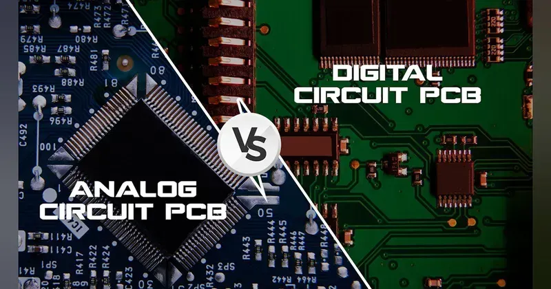
At the core of cutting-edge physics experiment demonstration boards lies impeccable PCB design, a domain where Zero One Solution Limited excels. Our profound expertise in PCB design for physics applications is not just about laying out traces; it's about engineering precision, ensuring signal integrity, and mitigating noise in the most demanding environments. We understand that the success of complex physics experiments hinges on the underlying electronic infrastructure, and our designs are meticulously crafted to meet these rigorous demands, driving innovation and accurate results.
| Design Area | Zero One Solution's Expertise | Impact on Physics Experiments |
|---|---|---|
| Sensitive Analog Circuits | Minimizing noise, high-precision signal conditioning, ultra-low drift designs for sensor interfaces. | Ensures accurate data acquisition from delicate sensors, crucial for precise measurements in experiments like quantum optics or material science. |
| High-Frequency Designs | Impedance matching, controlled impedance routing, parasitic inductance/capacitance reduction, RF/microwave considerations. | Preserves signal integrity for high-speed data transfer and radio frequency applications (e.g., spectroscopy, particle accelerators), preventing signal degradation and reflections. |
| Mixed-Signal Systems | Effective isolation between analog and digital domains, optimized grounding strategies, crosstalk mitigation. | Enables the seamless integration of control logic with precise measurement circuits, common in advanced experimental setups requiring both digital control and analog sensing. |
| Thermal Management | Optimized thermal vias, heat sinks integration, material selection for efficient heat dissipation. | Maintains stable operating temperatures for sensitive components, preventing drift and ensuring long-term reliability and accuracy of experimental results. |
| High-Density Interconnect (HDI) | Stacked microvias, fine line technology, compact component placement. | Allows for miniaturization and increased functionality in complex demonstration boards, crucial for integrating more features into a limited space. |
Our team of veteran engineers, leveraging two decades of experience from Silicon Valley, possesses a deep understanding of the unique challenges presented by physics applications. We go beyond standard design practices, employing advanced simulation tools and our proprietary design methodologies to address specific needs such as extreme temperature ranges, high electromagnetic interference environments, and ultra-low current measurements. This comprehensive approach ensures that every PCB we design for physics experiment demonstration boards is robust, reliable, and performs exactly as required for groundbreaking research and educational initiatives.
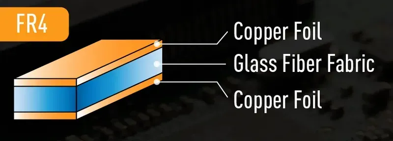
The choice of PCB material is a critical determinant of the performance, signal integrity, and long-term reliability of a physics experiment demonstration board. In complex experimental setups, where precise measurements and minimal interference are paramount, the dielectric properties, thermal conductivity, and mechanical stability of the substrate directly impact the accuracy and reproducibility of results. Selecting the appropriate material is not merely a design consideration but a fundamental requirement to ensure the board effectively fulfills its educational and research objectives, preventing signal loss, thermal runaway, and structural degradation that could compromise experimental integrity.
| Material Type | Key Properties | Typical Applications in Physics Boards | Advantages | Disadvantages |
|---|---|---|---|---|
| FR-4 (Standard Epoxy Glass) | Cost-effective, good electrical insulation, widely available | General purpose, low-frequency, non-critical signal paths | Low cost, good mechanical strength | Higher dielectric loss at high frequencies, less stable Dk/Df over temperature |
| Rogers Corporation Materials (e.g., RO4000 series) | Low dielectric loss (Df), stable dielectric constant (Dk) across frequencies and temperatures, excellent thermal stability | High-frequency RF/microwave circuits, sensitive analog front-ends, impedance-controlled lines | Superior signal integrity for high-speed/RF, low loss, excellent Dk stability | Higher cost than FR-4, can be more challenging to process |
| Teflon (PTFE/FEP based) | Extremely low dielectric loss, very stable Dk, excellent chemical resistance, wide operating temperature range | Ultra-high frequency (millimeter-wave), high-power applications, cryogenic experiments | Best-in-class electrical performance, highly stable, chemically inert | Very high cost, difficult to process (drilling, lamination), poor mechanical rigidity |
| Polyimide | High temperature resistance, excellent mechanical strength, good chemical resistance, flexible options available | High-temperature experiments, flexible circuits for compact setups, space applications | High thermal stability, good flexural endurance | Higher cost than FR-4, can absorb moisture more readily than other materials |
| Ceramic (e.g., Alumina) | Excellent thermal conductivity, very low dielectric loss, high temperature resistance, rigid | High-power circuits, power amplifiers, high-temperature sensors, integrated passive devices | Superior thermal management, excellent electrical performance at high temperatures | Brittle, high cost, limited board sizes, complex fabrication |
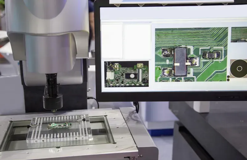
Ensuring the precision and reliability of Physics Experiment Demonstration Boards hinges critically on a meticulously controlled manufacturing process and stringent quality assurance. At Zero One Solution, our commitment to excellence translates into a multi-stage fabrication workflow, integrating cutting-edge technology and rigorous inspection protocols to guarantee PCBs that meet the exacting demands of scientific applications. This robust approach ensures every board performs flawlessly, providing accurate and repeatable experimental results essential for both education and advanced research.
| Quality Control Stage | Purpose | Technology Utilized | Benefit for Physics Boards |
|---|---|---|---|
| DFM Review | Proactive identification of manufacturing challenges | CAD analysis, expert engineering review | Ensures high yield and reliability for complex layouts |
| AOI (Automated Optical Inspection) | Detecting surface defects and inconsistencies | High-resolution cameras, image processing algorithms | Critical for maintaining signal integrity in sensitive circuits |
| X-Ray Inspection | Verifying hidden solder joints (BGAs, QFNs) | Computed tomography, digital radiography | Guarantees reliable connections for densely packed components |
| In-Circuit Testing (ICT) | Verifying electrical functionality of individual components and nets | Bed-of-nails fixtures, automated test programs | Confirms accurate component placement and electrical continuity |
| Functional Testing (FCT) | Simulating operational environment | Custom test jigs, specific input/output verification | Ensures the board meets its intended experimental purpose and performance criteria |
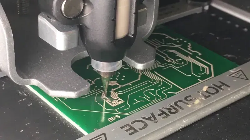
Rapid prototyping is a cornerstone of innovation, particularly for the intricate demands of Physics Experiment Demonstration Board Solutions. At Zero One Solution Limited, our rapid prototyping services are engineered to drastically shorten the design-to-deployment cycle, empowering researchers and educators to validate concepts, refine designs, and accelerate the development of groundbreaking physics demonstrations. This agility is critical in an environment where iterative refinement is key to achieving precise experimental setups and robust educational tools.
| Benefit | Impact on Physics Experiment Board Development | Traditional Prototyping Disadvantage |
|---|---|---|
| Accelerated Time-to-Market | Faster introduction of new experimental setups and educational tools. | Slow validation, delaying educational and research advancements. |
| Cost Efficiency | Reduced overall development costs through early error detection and optimization. | Increased expenses due to late-stage design flaws and repeated, lengthy cycles. |
| Enhanced Design Flexibility | Ability to experiment with various circuit configurations and component layouts. | Limited scope for innovation due to high cost and time investment per iteration. |
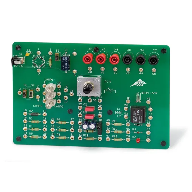
Zero One Solution has consistently delivered high-performance PCB solutions for a diverse range of physics experiment demonstration boards, enabling educators and researchers to bring complex theoretical concepts to life with tangible, reliable hardware. Our expertise shines in overcoming unique challenges inherent in these specialized applications, from managing intricate signal paths in quantum physics setups to ensuring robust power delivery in high-energy particle simulations. Through meticulous design, material selection, and advanced manufacturing, we transform conceptual models into functional, educational tools.
| Project Type | Challenge Overcome | Zero One Solution's Contribution | Impact on Education/Research |
|---|---|---|---|
| Quantum Entanglement Demonstrator | Mitigating signal noise and interference in picovolt-level measurements; ensuring precise phase coherence across multiple channels. | Designed custom multi-layer PCBs with optimized ground planes and differential routing, utilizing low-loss Rogers materials for superior signal integrity. Implemented advanced shielding techniques. | Enabled clearer visualization of quantum phenomena, enhancing student comprehension and facilitating advanced research into quantum computing principles. |
| Project Type | Challenge Overcome | Zero One Solution's Contribution | Impact on Education/Research |
|---|---|---|---|
| High-Energy Particle Detector Array | Handling high current transients and dissipating significant heat while maintaining component density and minimizing crosstalk. | Developed robust power distribution networks on heavy copper PCBs with integrated thermal vias. Optimized layout for efficient heat transfer and isolated sensitive analog front-ends. | Provided a stable, reliable platform for simulated particle detection, allowing for accurate data acquisition and analysis in educational settings. |
| Project Type | Challenge Overcome | Zero One Solution's Contribution | Impact on Education/Research |
|---|---|---|---|
| Optical Bench Alignment System | Achieving sub-micron precision for laser alignment and stability over extended periods in varying environmental conditions. | Fabricated ultra-flat PCBs with tight impedance control and specialized solder mask finishes to prevent light scattering. Employed selective gold plating for critical contact points. | Facilitated precise control over optical components, significantly reducing setup time for experiments and improving the accuracy of results in optics laboratories. |
| Project Type | Challenge Overcome | Zero One Solution's Contribution | Impact on Education/Research |
|---|---|---|---|
| Magnetic Field Mapping Device | Integrating sensitive magnetic sensors with high-speed data acquisition circuitry on a compact board, while minimizing electromagnetic interference (EMI). | Utilized advanced stacking and routing techniques for mixed-signal designs, incorporating dedicated analog and digital ground planes. Employed specific ferrite bead and capacitor placements for EMI suppression. | Delivered a highly accurate and compact device for visualizing complex magnetic fields, making abstract concepts concrete for students and researchers. |
| Project Type | Challenge Overcome | Zero One Solution's Contribution | Impact on Education/Research |
|---|---|---|---|
| Acoustic Resonance Chamber Controller | Ensuring precise frequency generation and measurement in a noisy acoustic environment, requiring robust signal filtering and amplification. | Designed PCBs with isolated analog and digital sections, implementing multi-stage active filters and robust power supply decoupling. Selected components with high SNR. | Enabled repeatable and accurate control of acoustic experiments, providing a reliable platform for studying sound wave phenomena and resonance. |
Choosing the right PCB solution provider is paramount for the success of physics experiment demonstration boards, which demand precision, reliability, and robust performance. Zero One Solution Limited stands as a beacon of excellence in this specialized field, offering a unique blend of technical prowess, rapid service delivery, and unwavering commitment to quality that translates directly into superior educational and research tools. Our comprehensive approach ensures that every demonstration board not only meets but exceeds the stringent requirements of advanced physics experimentation.
In conclusion, the development of physics experiment demonstration boards hinges on high-quality, reliable PCB solutions. Zero One Solution Limited stands at the forefront of this field, providing comprehensive services from initial design to final assembly. By choosing Zero One Solution, educators and researchers gain access to cutting-edge technology, rapid prototyping capabilities, and expert support, enabling them to create innovative and effective learning tools. Contact Zero One Solution today to discuss your PCB needs and accelerate the development of your next physics experiment demonstration board. Share this article with your colleagues and let us know your thoughts in the comments below!

