Revolutionizing Electronics: Choosing the Right Embedded Components PCB Manufacturer
2025.01.13
In today’s fast-paced tech world, the demand for smaller, more powerful electronic devices is ever-increasing. Embedded components PCB technology offers a revolutionary solution by integrating resistors, capacitors, and even active components directly within the circuit board layers, which leads to higher performance and miniaturization. This article will explore what this innovative process entails and guide you on selecting the right embedded components PCB manufacturer to bring your cutting-edge designs to life.
Understanding Embedded Components PCB Technology
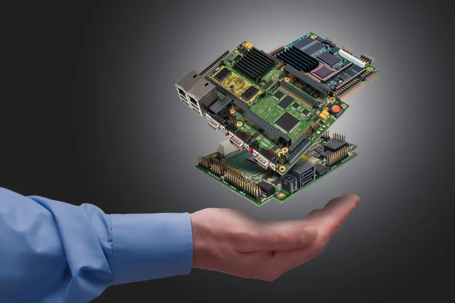
Embedded Components PCB
Embedded component PCB technology involves integrating electronic components within the inner layers of a printed circuit board (PCB), rather than mounting them on the surface. This contrasts with traditional surface mount technology (SMT), where components are soldered onto the outer layers of the PCB. Embedding components offers significant advantages, primarily in miniaturization and performance, and it is a key area of innovation in modern electronics manufacturing.
Key Concept: Layer Integration Embedded components are placed within the PCB substrate, becoming a part of the layered structure. This requires precise fabrication techniques to ensure proper electrical and mechanical integration.
Contrast with SMT Unlike SMT, where components are attached to the PCB surface post-fabrication, embedded components are integrated during the board manufacturing process itself.
Advantages over Traditional Methods The primary benefits include reduced board size, improved electrical performance due to shorter interconnects, and enhanced thermal management by utilizing the board's inner layers as a heat sink.
Feature
Embedded Components PCB
Surface Mount Technology (SMT)
Component Placement
Integrated within PCB layers
Mounted on PCB surface
Board Size
Smaller, more compact
Larger, less dense
Electrical Performance
Improved due to shorter interconnects
Potentially limited by longer traces
Thermal Management
Enhanced, with PCB layers acting as heatsinks
Can require additional heatsinks
Manufacturing Process
More complex, integrated process
Less complex, separate assembly process
Benefits of Using Embedded Components in PCBs
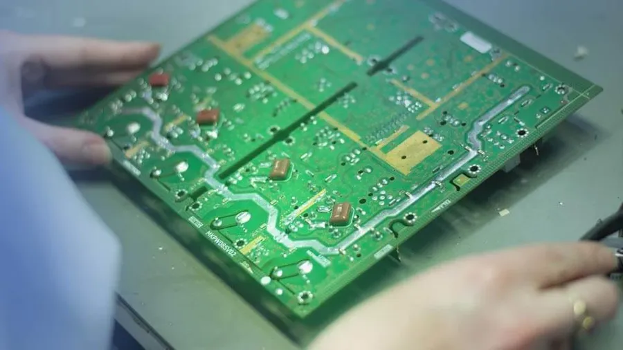
PCB Internal Components
Embedding components within printed circuit boards (PCBs) offers significant advantages over traditional surface mount technology (SMT), fundamentally altering how electronic devices are designed and manufactured. These benefits encompass reduced size, improved electrical performance, enhanced thermal management, and increased reliability, all contributing to more efficient and robust electronic systems.
Benefit
Description
Impact on Electronic Device Design
Reduced Size
Embedding components within internal layers of the PCB allows for a higher density of components, minimizing the overall footprint of the board.
Enables smaller and more compact electronic devices, crucial for applications with stringent size constraints such as wearables and IoT devices.
Improved Electrical Performance
Shorter interconnects and controlled impedance achieved through embedded components result in reduced signal path lengths and parasitic inductances.
Enhances signal integrity, reduces signal loss, and enables higher operating frequencies and faster data transfer rates.
Enhanced Thermal Management
Embedded components facilitate more direct heat dissipation paths to internal layers of the PCB, often incorporating thermal vias and conductive planes.
Reduces hot spots and improves overall heat distribution across the PCB, crucial for high-power applications and preventing component failures.
Increased Reliability
Components are protected within the PCB structure, shielding them from environmental factors and mechanical stress.
Increases the robustness and lifespan of the electronic system, reducing failures and maintenance.
The benefits of embedding components in PCBs extend beyond individual component performance and contribute to a more streamlined and robust manufacturing process, which is becoming increasingly important in high-performance electronic products.
Types of Components Embedded in PCBs
Embedded Resistors and Capacitors
Embedded component technology in PCBs enables the integration of various passive and active components directly within the substrate layers, offering a higher level of miniaturization and performance. This approach differs significantly from traditional surface mount technology (SMT) by incorporating components during the PCB fabrication process. This allows for a more compact design and improved performance characteristics.
Component Type
Description
Typical Materials
Common Use Cases
Resistors
Provide a defined resistance to electrical current flow.
Thick-film pastes, thin-film materials
Current limiting, voltage division
Capacitors
Store electrical energy in an electric field.
Ceramic materials, polymer films
Bypassing, decoupling, filtering
Inductors
Store energy in a magnetic field and resist changes in current.
Copper coils, ferrite materials
Filtering, impedance matching
Diodes
Allow current flow in one direction.
Silicon, Gallium Arsenide
Rectification, signal modulation
Transistors
Semiconductor devices used to switch or amplify electronic signals and electrical power.
Silicon, Germanium
Switching, amplification
Integrated Circuits (ICs)
Complex circuits built on a single semiconductor chip, often containing multiple transistors and other elements.
Silicon
Complex logic, memory, signal processing
The selection of materials is crucial for embedded components, as these materials must be compatible with the PCB fabrication processes and provide stable electrical characteristics across operating temperatures and environmental conditions. Material choices are driven by factors including electrical conductivity, dielectric strength, and thermal properties. For example, thick-film pastes with specific resistivity characteristics can be used for embedded resistors, while ceramic-based dielectrics are common for embedded capacitors. The materials need to be able to withstand the temperatures and pressures of the lamination process.
Selecting a Reliable Embedded Components PCB Manufacturer
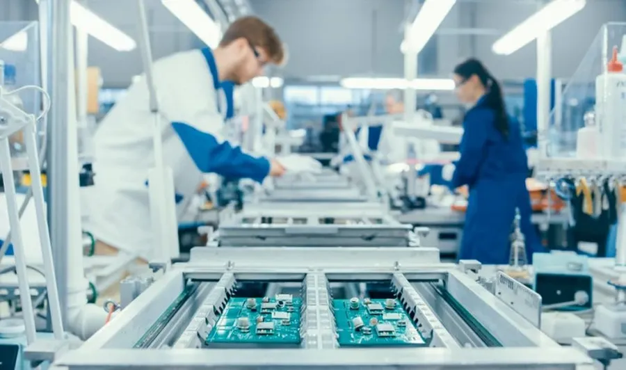
PCB Manufacturing Facility
Choosing the right embedded components PCB manufacturer is paramount for ensuring the success of any electronic product integrating this advanced technology. The selection process should be thorough, encompassing a manufacturer's technological capabilities, adherence to quality standards, possession of relevant certifications, and ability to meet required turnaround times.
This section delves into the critical evaluation criteria essential for selecting a manufacturer capable of delivering high-quality, reliable embedded PCB solutions. A collaborative partnership with a capable manufacturer is not just beneficial, it's often essential for projects of this kind.
Technology Capabilities A suitable manufacturer must possess advanced manufacturing technologies and techniques specifically tailored for embedded components. This includes precision placement equipment, thin core lamination, microvia drilling, and specialized plating processes. Verify the manufacturer's proficiency in handling specific component types and material requirements that match your design.
Quality Standards and Control A manufacturer's adherence to rigorous quality standards is a non-negotiable aspect. Seek manufacturers that are certified according to industry standards like ISO 9001, IPC-A-600, and others that are relevant. Investigate their quality control procedures, such as in-process inspection and testing, and inquire about their defect rate. A robust quality system directly translates to higher reliability and less risk of failure.
Relevant Certifications Beyond basic quality standards, look for specific certifications that attest to a manufacturer’s proficiency with embedded components technology. Certifications such as those related to specific material handling, cleanliness standards, or high-reliability assembly can provide added confidence in a manufacturer's capabilities.
Turnaround Time and Production Capacity Assess the manufacturer's ability to meet your production timeline. Evaluate their production capacity, lead times for prototypes and mass production, and responsiveness to schedule changes. A manufacturer with sufficient capacity and flexibility to meet the project's specific demands is crucial for keeping a project on track.
Experience and Expertise A manufacturer's experience in embedded components is an important factor. Their past projects, client references, and any case studies that highlight expertise in this specialized field are good indicators of the manufacturer’s proficiency and can help in predicting their ability to successfully handle your requirements. Partnering with an experienced manufacturer greatly mitigates risks and improves the chances of success.
Communication and Collaboration Effective communication between the design team and the manufacturer is vital. Evaluate the communication channels the manufacturer utilizes and their responsiveness to queries and issues. A partner that can offer technical support and work collaboratively in all stages of the project is beneficial for problem-solving and project success.
Cost Analysis Cost is always an important aspect to consider. However, it is important to balance cost with quality, reliability, and a manufacturer’s experience. Seek a manufacturer that can provide a cost-effective solution without jeopardizing the quality of the embedded components PCB.
Embedded PCB Manufacturing Processes
PCB Lamination Process
The fabrication of embedded component PCBs involves a series of sophisticated processes, each critical to ensuring the functionality and reliability of the final product. These processes go beyond standard PCB manufacturing techniques, integrating component placement directly within the PCB's layers.
Key manufacturing steps include:
Thin Core Technology: Utilizing very thin core materials is fundamental to enabling the embedding of components. These materials provide the necessary substrate for component placement and interconnection within the PCB layers, demanding precision in material handling and processing.
Cavity Formation: Creating cavities or recesses within the PCB is essential to accommodate the embedded components. This process requires high precision techniques, often involving laser ablation or controlled depth etching, to ensure accurate component placement and alignment.
Precision Printing: This step involves the precise deposition of conductive inks and materials to form the interconnections and conductive pathways. High resolution printing techniques, like inkjet printing or screen printing, are used to guarantee accurate pattern transfer and electrical performance of the internal circuitry.
Component Placement: Components are placed into the formed cavities using automated pick-and-place equipment specifically designed for handling and positioning of small and often delicate embedded components. Accuracy is paramount, with advanced vision systems often used to ensure precise placement.
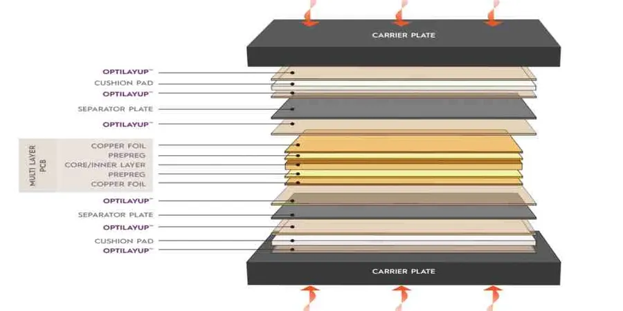
Lamination: The lamination process is used to encapsulate the embedded components, and create the multilayer structure. This involves applying heat and pressure to bond the layers, ensuring that embedded components are securely enclosed and protected. Proper lamination control is vital for maintaining structural integrity and performance.
Interconnection Formation: The interconnections from the embedded components are connected to the circuits of the next layer by via formation and subsequent plating. This step creates electrical links for the whole circuit.
Final Inspection and Testing: Rigorous testing, including electrical testing and X-ray inspection, is conducted to verify the integrity and functionality of the embedded components and interconnections. This ensures that each manufactured PCB meets the desired specifications and performance criteria, leading to a reliable end-product.
Frequently Asked Questions About Embedded Components PCBs
This section addresses common questions regarding embedded components in PCBs, offering precise and concise answers to assist in understanding this advanced technology. These FAQs cover essential aspects, from basic definitions to manufacturing considerations.
What are embedded components in PCBs? Embedded components in PCBs are electronic components, such as resistors, capacitors, inductors, and even integrated circuits, that are placed within the inner layers of a printed circuit board during the manufacturing process, rather than being mounted on the surface. This differs significantly from traditional surface mount technology (SMT).
Why embed components within a PCB? Embedding components offers several key advantages, including: reduced overall device size, improved electrical performance due to shorter interconnects, enhanced thermal management by distributing heat more evenly, and increased reliability due to the components being protected within the board structure. It facilitates higher component densities than standard SMT.
What types of components can be embedded in PCBs? A variety of components can be embedded, including passive components like resistors, capacitors, and inductors. Active devices such as diodes, transistors, and even integrated circuits can be embedded with proper design and manufacturing considerations, and selecting components based on their size, material compatibility and thermal endurance.
Who are the leading manufacturers of embedded components PCBs? Identifying the 'best' manufacturer depends largely on specific project needs, including technology requirements, volume, and quality certifications. However, several reputable manufacturers are known for their capabilities in this area; typically the manufacturers who support advanced technologies such as HDI, flexible or rigid-flex PCBs will have experience in embedded components. It is recommended to evaluate potential partners based on their specific technological capabilities, quality standards, and relevant certifications for your project.
What are the key manufacturing processes for embedded PCBs? Key processes include precision printing of conductive layers, embedding components using pick-and-place or similar technologies, lamination of layers using heat and pressure, microvia formation for interlayer connections, and precision etching to create the desired patterns. Accurate registration and controlled parameters are critical at each step to maintain reliability.
Are embedded component PCBs more expensive than standard PCBs? Initially, embedded component PCBs can involve higher costs due to more complex materials and processes, involving higher precision. However, the reduction in overall size, increased performance, and higher reliability often lead to long-term cost savings in terms of reduced component count, more efficient designs, and lower failure rates in the field.
What is the reliability of embedded components? Embedded components are typically more reliable due to the protection offered by being encapsulated within the PCB layers. This shields them from environmental factors and mechanical stress, improving their operational longevity and reduces the risk of connection failures.
Cost Considerations for Embedded Components PCBs
The cost of embedded component PCBs is a multifaceted issue, encompassing initial expenses in materials and manufacturing but potentially delivering significant long-term savings through enhanced performance and reliability. Understanding these cost factors is crucial for making informed decisions about incorporating this advanced technology into electronic designs.
Several factors influence the overall cost of embedded component PCBs:
Material Costs Specialized dielectric materials, conductive inks, and the embedded components themselves contribute to the initial material cost. The quality and type of these materials directly affect both the price and performance of the final product.
Tooling and Setup Producing embedded PCBs requires precision tooling, advanced manufacturing equipment, and meticulous setup procedures, especially when dealing with ultra-fine geometries or multiple layer embedding. These upfront investments can be substantial but are essential for consistent high-quality output.
Manufacturing Complexity The intricate nature of embedding components within the PCB layers necessitates specialized processes such as thin core technology, precision lamination, and laser micro-machining. These processes increase manufacturing complexity, consequently influencing the cost. The more layers of embedding there are and the finer the tolerances, the higher the manufacturing cost will be.
Assembly Costs While embedding components can reduce the need for some surface mount processes, specialized assembly techniques may still be required for other components. Additionally, the precise nature of embedded structures demands robust inspection and testing procedures.
While the initial investment for embedded component PCBs might appear higher than traditional PCBs, the long-term advantages can justify this expenditure. The benefits include:
Reduced System Size Embedding components leads to smaller, more compact circuit board designs. This can translate to lower material usage and reduced overall costs in the broader product.
Improved Electrical Performance The shorter signal paths inherent in embedded designs can lead to enhanced performance, reduced signal interference, and better overall circuit operation. This reduction in interference and improvement in performance increases efficiency and longevity and thus reduces long term costs.
Enhanced Reliability Embedded components are protected from external factors like moisture and mechanical stress, leading to higher reliability and a longer product lifespan. This results in lower warranty costs and reduces overall costs associated with failures.
Improved Thermal Management Embedding components often improves the thermal dissipation within the device, which can reduce the need for bulky heat sinks and potentially lower thermal management costs.
In conclusion, cost considerations for embedded component PCBs must take into account both upfront expenditures and the potential long-term gains through performance, reliability, and size advantages. Evaluating these factors is essential in making an economically sound decision about whether to adopt this advanced technology.
Future Trends in Embedded Components PCB Technology
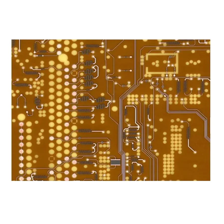
Flexible Embedded PCB
The field of embedded components PCB technology is rapidly evolving, driven by the demand for smaller, more efficient, and higher-performing electronic devices. Future trends point towards significant advancements in materials, manufacturing processes, and component integration, promising to revolutionize the design and capabilities of next-generation electronics.
Advanced Materials Integration The integration of novel materials with enhanced electrical, thermal, and mechanical properties is a key focus. This includes the use of nano-materials, advanced polymers, and ceramics to achieve higher component densities and improved performance characteristics. The development of materials that offer superior heat dissipation and reduced signal loss is particularly critical for high-frequency applications.
Finer Geometries and High-Density Interconnects The push for miniaturization requires the ability to manufacture PCBs with finer lines, spaces, and vias. Advanced lithography techniques, along with innovations in etching and plating, are crucial for creating high-density interconnects (HDI) and microvias with greater precision. These developments facilitate the integration of more components into smaller areas, enabling the production of compact and powerful devices.
3D Integration Techniques Moving beyond traditional 2D PCB designs, 3D integration is gaining traction. Techniques like through-silicon vias (TSVs) and stacked die technology enable the vertical stacking of components and interconnects within a PCB, further reducing the footprint and increasing functional density. These advancements are essential for creating highly integrated and compact electronic systems.
Enhanced Reliability and Durability Future trends also emphasize improved reliability and durability for embedded component PCBs. This includes the development of more robust manufacturing processes and materials that can withstand harsh environmental conditions such as extreme temperatures, humidity, and vibration. Enhanced reliability is crucial for applications in automotive, aerospace, and industrial sectors.
AI-Driven Design and Manufacturing Artificial intelligence (AI) and machine learning (ML) are increasingly being applied in PCB design and manufacturing. AI-powered tools can automate design processes, optimize layouts for performance and manufacturability, and predict potential issues before they arise. ML algorithms can also enhance process control and improve yields by learning from manufacturing data. This integration of AI will accelerate development cycles and improve overall efficiency.
Sustainable Manufacturing Practices There is a growing emphasis on sustainable manufacturing practices in the PCB industry. This involves the use of eco-friendly materials, reduction of waste, and the adoption of energy-efficient processes. The use of recyclable materials, water-based solvents, and closed-loop manufacturing systems is gaining popularity. This move towards more sustainable methods helps reduce the environmental impact of electronics manufacturing.
Embedded components PCB technology is reshaping the landscape of electronics, offering significant benefits in performance, size, and reliability. By understanding the intricacies of this technology and carefully selecting an experienced embedded components PCB manufacturer, you can leverage these advantages to create innovative and highly competitive electronic products. Partnering with a skilled pcb manufacturer is crucial to bring these complex designs to market successfully and efficiently. The future of electronics is built on embedded technology, and the right partner will guide you to its full potential.