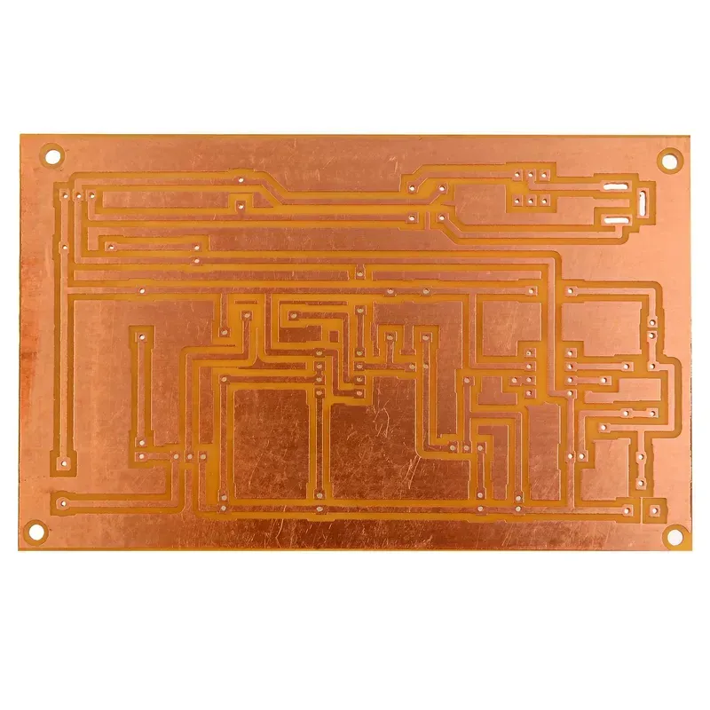
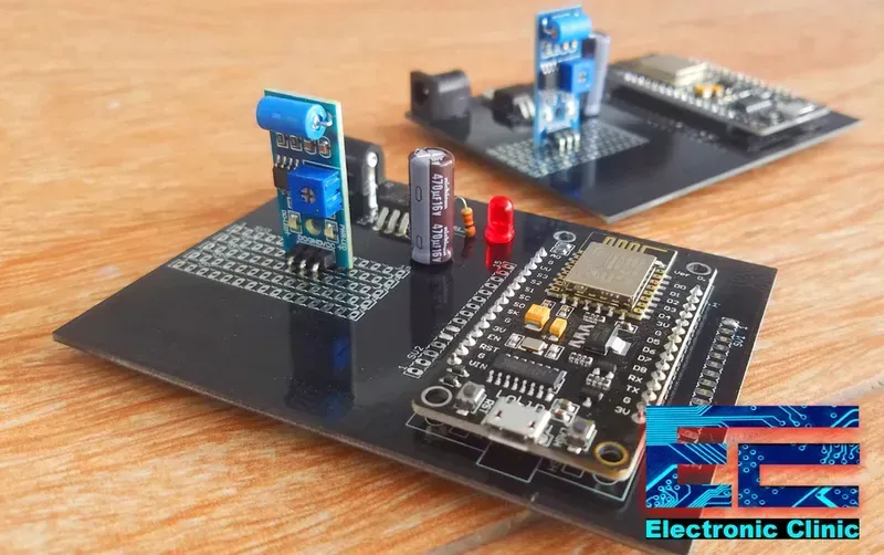
In the realm of geophysics, seismic monitoring stations stand as sentinels, vigilantly listening for the subtle tremors and powerful upheavals that shape our planet. These sophisticated systems rely heavily on the accuracy and reliability of their electronic components, particularly the Printed Circuit Boards (PCBs) that form their central nervous system. At Zero One Solution Limited, we understand the critical role these PCBs play, and we offer comprehensive PCB solutions tailored specifically for seismic monitoring applications. This article delves into the intricacies of designing, manufacturing, and assembling PCBs for seismic monitoring stations, highlighting the key considerations and innovative approaches that ensure optimal performance and data integrity.
Introduction: The Vital Role of PCBs in Seismic Monitoring
Seismic monitoring stations are critical infrastructure for understanding Earth's dynamic processes, from detecting earthquakes and volcanic activity to monitoring structural integrity in engineering projects. At the core of their sophisticated operation are Printed Circuit Boards (PCBs), which serve as the central nervous system for data acquisition, signal processing, and communication. The reliability and precision of these PCBs directly dictate the accuracy and continuity of seismic data, making their design and manufacturing paramount. Zero One Solution Limited, with over a decade of expertise in rapid prototyping and one-stop PCB solutions, understands these stringent demands, providing robust and high-performance PCBs essential for dependable seismic monitoring systems.
What are seismic monitoring stations? Seismic monitoring stations are sophisticated installations equipped with seismometers and other sensors to detect and record ground motion caused by seismic waves. These stations play a crucial role in earthquake early warning systems, geological research, and resource exploration by providing real-time data on seismic events globally. Their continuous operation relies heavily on the reliability of their embedded electronic systems, primarily driven by high-quality PCBs.
Function
PCB's Critical Role
Impact of PCB Failure
Data Acquisition
Analog-to-digital conversion, sensor interfacing
Loss of crucial seismic data
Signal Processing
Noise filtering, amplification, data aggregation
Corrupted or inaccurate data analysis
Communication
Data transmission to central processing units
Breakdown in real-time alert systems
Power Management
Efficient power distribution to components
System instability and potential shutdowns
The operational environment for seismic monitoring stations can be extremely challenging, often involving remote locations with varying temperatures, humidity, and potential electromagnetic interference. This necessitates PCBs that are not only high-performing but also exceptionally durable and resilient. Zero One Solution Limited leverages its extensive experience in advanced PCB fabrication and assembly to produce boards that withstand these harsh conditions, ensuring long-term operational stability and data integrity for critical seismic applications.
Key Design Considerations for Seismic Monitoring PCBs
Designing Printed Circuit Boards (PCBs) for seismic monitoring stations demands a meticulous approach, prioritizing unwavering reliability and precision under extreme conditions. The core challenge lies in capturing minute seismic signals accurately while withstanding environmental stressors like temperature fluctuations, moisture, and vibrations. Effective PCB design for these critical applications hinges on addressing fundamental principles such as signal integrity, noise reduction, and robust thermal management to ensure continuous, high-fidelity data acquisition.
Signal Integrity and Noise Reduction Maintaining signal integrity is paramount for accurate seismic data. This involves careful trace routing to minimize impedance mismatches and crosstalk, ensuring that delicate sensor signals are not corrupted. Techniques like differential signaling, controlled impedance traces, and strategic placement of decoupling capacitors are employed to achieve high signal-to-noise ratios. Furthermore, implementing proper grounding strategies, such as star grounds or ground planes, effectively mitigates common-mode noise and electromagnetic interference (EMI), which can severely compromise data quality in sensitive seismic instrumentation. Shielding critical components and sensitive signal paths also plays a vital role in preventing external noise ingress, crucial for distinguishing subtle seismic events from background interference. Zero One Solution Limited leverages advanced simulation tools to optimize layouts for superior signal performance, guaranteeing the fidelity of critical seismic data streams.
Material Selection for Harsh Environments The operational environment of seismic monitoring stations often includes remote, unconditioned locations exposed to significant temperature extremes, humidity, and mechanical stress. Therefore, selecting PCB substrate materials with excellent thermal stability, low moisture absorption, and robust mechanical properties is crucial. Materials such as high-Tg FR-4, polyimide, or specialized ceramic-filled laminates offer superior performance in these demanding conditions compared to standard FR-4. These materials minimize dimensional changes due to temperature variations, reducing stress on components and interconnections, and ensuring long-term reliability. Zero One Solution Limited guides clients in selecting optimal materials, considering factors like dielectric constant stability across temperature ranges and chemical resistance to environmental contaminants, ensuring the PCB's longevity and consistent performance.
Thermal Management Strategies Seismic monitoring equipment, especially processors and data acquisition modules, generates heat that, if not effectively dissipated, can lead to component degradation, performance drift, or outright failure. Robust thermal management is indispensable to maintain operational stability and extend the lifespan of the PCB. Strategies include incorporating thick copper layers for improved heat spreading, utilizing thermal vias to transfer heat to ground planes or heatsinks, and strategically placing heat-generating components to optimize airflow within the enclosure. For high-power components, dedicated heatsinks or even active cooling solutions might be integrated. Zero One Solution Limited employs thermal simulation software to analyze heat distribution and optimize PCB layouts for efficient thermal dissipation, preventing hot spots and ensuring components operate within their specified temperature limits, vital for reliable, continuous seismic data collection.
Material Selection: Ensuring Reliability in Extreme Conditions
The operational integrity of printed circuit boards (PCBs) in seismic monitoring stations is fundamentally reliant on the meticulous selection of materials, given the extreme environmental conditions they must endure. From vast temperature fluctuations to high humidity and vibrational stress, the chosen substrate, laminate, and copper foil significantly dictate the long-term reliability and accuracy of the collected seismic data. At Zero One Solution Limited, our material selection process is a rigorous exercise in engineering precision, focusing on characteristics such as superior thermal stability, low dielectric loss, and excellent moisture resistance to guarantee unwavering performance.
Material Type
Key Properties
Typical Seismic Application Suitability
FR-4 (Standard Epoxy Glass)
Cost-effective, good electrical and mechanical properties, widely available.
General-purpose monitoring, less extreme environments, non-critical signal paths where cost is a primary driver. Good for base layers or less sensitive circuits due to its balance of performance and cost, though thermal and moisture limitations need consideration for outdoor, exposed applications without proper enclosure and environmental control strategy. It performs best indoors or in controlled environments
Applications with significant power dissipation or higher operating temperatures, ensuring dimensional stability and reliability under thermal stress. Ideal for densely populated boards where heat generation from components is a concern. Recommended when the operational temperature range exceeds the capabilities of standard FR-4, as seen in stations with intensive data processing units or power management circuits
Rogers (PTFE/Ceramic/Hydrocarbon)
Low dielectric constant (Dk) and dissipation factor (Df), excellent high-frequency performance, stable over temperature.
RF and microwave circuits, high-speed data acquisition, antenna systems where signal integrity and minimal signal loss are paramount. Essential for precise signal transmission from sensitive seismic sensors to data converters, where any signal degradation can compromise the accuracy of seismic event detection and analysis. Its low Dk and Df ensure that signal propagation speeds are consistent and losses are minimized, crucial for maintaining timing and amplitude accuracy in high-frequency seismic signals
Polyimide
Exceptional thermal resistance, chemical resistance, mechanical flexibility (in flex/rigid-flex forms).
High-temperature environments, critical components requiring extreme durability, flexible interconnections in constrained spaces. Excellent for applications exposed to extreme temperature variations or requiring repeated flexing, offering a high degree of reliability in harsh, dynamic environments. Its superior thermal properties make it suitable for deep-borehole seismic sensors or applications in geothermally active regions. Can also be used as a prepreg material in multilayer PCBs to enhance overall board reliability and reduce delamination risk under thermal cycling
Ceramic/Alumina
Extremely high thermal conductivity, low CTE, excellent electrical insulation.
Power modules, high-frequency modules, extreme temperature environments. Used as a substrate for power amplifier modules or high-temperature sensor interfaces, offering superior heat dissipation and mechanical stability where component temperature control is critical. Ideal for circuits that generate significant heat and require active cooling or are exposed to very high ambient temperatures, providing a stable platform for heat-sensitive components.
Beyond the primary substrate, critical consideration is given to the copper foil thickness, determined by the current carrying requirements and the need for impedance control. Additionally, solder mask and surface finishes like ENIG (Electroless Nickel Immersion Gold) or OSP (Organic Solderability Preservative) are selected for their protective qualities against oxidation, corrosion, and to ensure reliable solder joint formation under varied climatic conditions. This multi-faceted approach to material selection underscores our commitment to delivering seismic monitoring PCB solutions that are not only high-performing but also supremely resilient and reliable.
Advanced PCB Manufacturing Techniques for Precision and Durability
PCB Etching Process
Precision and durability are paramount for PCBs operating within seismic monitoring stations, demanding advanced manufacturing techniques that go beyond standard practices. The effectiveness of a seismic monitoring station hinges on its ability to capture subtle ground movements with unwavering accuracy and withstand environmental stressors. This necessitates manufacturing processes that ensure exceptional signal integrity, robust mechanical stability, and long-term reliability. Zero One Solution Limited leverages state-of-the-art fabrication methodologies to meet these exacting requirements, guaranteeing that every PCB can perform flawlessly under the most demanding conditions.
High-Precision Etching for Fine Traces Our manufacturing employs advanced etching techniques, such as differential etching and plasma etching, to achieve ultra-fine traces and spaces. This precision is critical for high-density interconnect (HDI) designs prevalent in seismic monitoring equipment, minimizing signal loss and ensuring precise data transmission. Control over etch uniformity is paramount to avoid impedance variations that could distort sensor readings.
Laser Drilling for Microvias For multi-layer PCBs in seismic applications, traditional mechanical drilling is often insufficient. We utilize laser drilling technology to create microvias, enabling higher circuit density and improved signal paths in compact designs. This technique reduces overall board size while enhancing performance and allowing for more complex component integration, essential for advanced sensor arrays.
Controlled Plating for Robust Connections The plating process is meticulously controlled to ensure uniform copper deposition within vias and on traces. Advanced plating solutions, including electroless and electrolytic plating, are used to create robust and reliable interconnections capable of enduring mechanical stress and temperature fluctuations. This prevents delamination and ensures long-term electrical conductivity in harsh environments.
Manufacturing Stage
Key Technique
Benefit for Seismic PCBs
Fabrication
Direct Imaging (DI)
Enhanced precision for complex trace geometries and improved signal integrity. Ensures consistent layer alignment for reliable performance in sensitive applications like seismic monitoring where data accuracy is critical and signal distortion must be minimized. Reduces the risk of short circuits and open circuits, contributing to overall board reliability and longevity under continuous operation in harsh environments, including those with significant vibrations or temperature fluctuations.
Drilling
Laser Drilling for Microvias
Enables higher component density and shorter signal paths, crucial for compact seismic sensors. This method also minimizes mechanical stress on the board, leading to greater durability and resistance to fatigue failure, which is especially important for equipment subjected to constant seismic activity or environmental vibrations.
Plating
Electroless Nickel Immersion Gold (ENIG)
Provides excellent solderability and protects exposed copper from oxidation, enhancing long-term reliability in varying climatic conditions. The flat surface finish is ideal for fine-pitch components often used in seismic data acquisition, preventing issues during assembly and ensuring stable electrical connections. Enhances the board's resistance to corrosion, a key factor for outdoor or underground seismic installations where moisture and other environmental contaminants are present, thereby extending the operational lifespan of the monitoring equipment.
Solder Mask Application
Liquid Photoimageable (LPI) Solder Mask
Offers precise application and excellent adhesion, protecting circuits from environmental damage and shorting. Its high resolution supports fine-pitch component assembly and prevents solder bridging, which is vital for high-reliability systems like those used in seismic monitoring that must operate error-free for extended periods without maintenance.
Quality control is integrated at every stage of our manufacturing process. We employ Automated Optical Inspection (AOI) to detect subtle defects, X-ray inspection for internal layer alignment and drill registration, and electrical testing to verify circuit continuity and insulation resistance. These rigorous checks guarantee that every PCB meets the stringent performance and durability specifications required for seismic monitoring stations, providing an uncompromised foundation for accurate and reliable data collection.
Component Placement and Layout Strategies for Optimal Performance
Seismic Sensor PCB Layout
In the demanding realm of seismic monitoring, the performance of a PCB is not solely determined by its robust materials or advanced manufacturing; equally critical are the meticulous strategies employed for component placement and layout. Precision in these aspects is paramount to ensuring accurate data acquisition, minimizing signal interference, and maintaining the integrity of sensitive sensor readings. Effective layout mitigates electromagnetic interference (EMI) and crosstalk, which can severely degrade the fidelity of the minute seismic signals, directly impacting the station's ability to detect and analyze ground movements with the required accuracy.
Minimizing Signal Interference and Crosstalk Signal integrity is foundational for seismic data. We employ differential signaling for critical data paths, routing traces parallel and tightly coupled to cancel out common-mode noise. Guard traces and proper spacing between signal lines are utilized to minimize capacitive and inductive coupling, effectively reducing crosstalk. For high-frequency signals, controlled impedance routing is strictly adhered to, preventing reflections and maintaining signal fidelity across the board. This meticulous approach ensures that the tiny electrical signals from seismic sensors are accurately transmitted and processed without corruption from neighboring traces.
Optimal Placement of Sensitive Components for Accurate Data Acquisition Sensitive analog components, such as Analog-to-Digital Converters (ADCs) and low-noise amplifiers, are strategically placed to be as close as possible to the input connectors and sensors. This minimizes the length of analog signal traces, thereby reducing their susceptibility to noise pick-up and impedance mismatches. Digital components and power supply circuits are isolated from analog sections using dedicated ground planes and careful component orientation to prevent their switching noise from affecting the sensitive analog front end. Thermal considerations also guide placement, ensuring heat-generating components are positioned to allow for efficient dissipation, preventing localized hot spots that can introduce drift or inaccuracy in sensitive measurements.
Grounding Techniques to Reduce Noise and Improve Signal Integrity A robust grounding strategy is indispensable for noise reduction. We implement multi-layer PCBs with dedicated ground planes to provide low-impedance return paths for all signals, minimizing ground bounce and common-mode noise. Star grounding techniques are employed for sensitive analog circuits, ensuring that each critical component has a direct, dedicated path to a central ground point, preventing ground loops. Stitching vias are liberally used to connect different ground planes, creating a contiguous ground reference across all layers. This comprehensive grounding approach effectively shunts noise to ground, preserving the signal-to-noise ratio critical for reliable seismic data.
PCB Assembly and Testing: Guaranteeing Functionality and Longevity
SMT PCB Assembly
The meticulous assembly and rigorous testing of Printed Circuit Boards (PCBs) are paramount in ensuring the functionality, reliability, and longevity of seismic monitoring stations. Even the most impeccably designed PCB will fail without precise assembly and comprehensive validation under simulated operational stresses. At Zero One Solution Limited, our advanced assembly capabilities and multi-stage testing protocols are engineered to deliver PCBs that withstand the demanding conditions inherent in seismic monitoring, thereby guaranteeing consistent and accurate data acquisition.
Advanced PCB Assembly Techniques We employ a diverse range of assembly techniques to meet the specific requirements of seismic monitoring PCBs, which often feature a mix of high-precision components. Surface Mount Technology (SMT) offers high component density and automated placement, crucial for compact seismic sensors. Through-Hole Technology (THT) is utilized for robust components requiring stronger mechanical bonds, such as connectors and power regulation circuitry, ensuring durability against vibrations. Our mixed technology approach optimally combines SMT and THT on a single board, leveraging the strengths of both for complex seismic applications.
Automated Optical Inspection (AOI) AOI is a critical non-contact inspection method used early in the assembly process to identify defects such as missing components, incorrect polarity, solder bridges, and shorts. Utilizing high-resolution cameras and advanced algorithms, AOI ensures that component placement is precise and solder joints are defect-free, significantly reducing the likelihood of costly reworks and enhancing overall reliability before functional testing begins.
In-Circuit Testing (ICT) ICT is a powerful diagnostic tool that electrically tests individual components and circuit nodes on the assembled PCB. By applying test signals and measuring responses, ICT can detect manufacturing defects like opens, shorts, resistance, capacitance, and component functionality issues. This comprehensive electrical verification ensures that each circuit on the seismic monitoring PCB operates as designed, providing a high level of confidence in the board's integrity.
Functional Testing and Environmental Simulation Beyond initial electrical checks, seismic monitoring PCBs undergo rigorous functional testing to validate their performance under real-world operating conditions. This includes simulating varying temperatures (thermal cycling), humidity levels, and vibrational stresses to expose potential weaknesses or intermittent failures. Such environmental testing, including burn-in processes, accelerates the aging of components and boards, guaranteeing their longevity and stable operation in the challenging outdoor or remote environments typical of seismic stations.
Quality Control and Traceability Our commitment to quality extends to comprehensive traceability protocols. Each PCB undergoes stringent quality checks at every stage of assembly and testing, with detailed records maintained for materials, processes, and test results. This ensures complete transparency and allows for rapid identification and resolution of any issues, upholding the highest standards for critical applications like seismic monitoring.
Zero One Solution Limited: Your Partner for Seismic Monitoring PCB Solutions
Finished Seismic Monitoring Station PCB
At Zero One Solution Limited, we understand the critical demands of seismic monitoring, where the reliability and precision of printed circuit boards are paramount. Leveraging over a decade of expertise and a strategic global presence, we offer a comprehensive, one-stop solution for the entire PCB lifecycle – from design and rapid prototyping to manufacturing and assembly – specifically tailored for the stringent requirements of seismic monitoring stations. Our commitment to cutting-edge technology and rigorous quality control ensures that your seismic instruments are equipped with PCBs engineered for unparalleled performance and longevity in even the most challenging environments.
Full-Spectrum PCB Design & Engineering Our seasoned engineers provide expert design services, optimizing layouts for superior signal integrity, noise reduction, and thermal management, crucial for sensitive seismic data acquisition. We integrate advanced features and adhere to industry standards, ensuring your PCBs are robust and reliable.
Rapid Prototyping for Accelerated Development Understanding the fast-paced nature of R&D, Zero One Solution Limited specializes in rapid prototyping. We compress development cycles, enabling quick iterations and validation of your seismic monitoring PCB designs, significantly reducing your time-to-market.
Precision Manufacturing with Global Reach Headquartered in Shenzhen with a branch in Dubai, we harness a sophisticated global supply chain network for manufacturing. Our facilities utilize advanced techniques for etching, drilling, and plating, guaranteeing the precision and durability required for high-performance seismic applications.
Advanced Assembly & Rigorous Testing From SMT and through-hole assembly to mixed technologies, our state-of-the-art assembly lines ensure impeccable component placement. Every PCB undergoes comprehensive testing, including Automated Optical Inspection (AOI), In-Circuit Testing (ICT), and environmental simulations, to validate functionality and ensure long-term reliability in harsh conditions.
Seamless One-Stop Service & Supply Chain Management Eliminate the complexities of managing multiple vendors. Zero One Solution Limited offers an integrated one-stop solution, streamlining your entire PCB procurement process from initial concept to final delivery. Our robust supply chain management ensures timely delivery and cost-effectiveness.
Service Area
Key Benefit for Seismic Monitoring PCBs
Zero One Solution Advantage
PCB Design
Optimized for signal integrity, low noise, and environmental resilience
Deep expertise in sensor interface and data acquisition circuits
Rapid Prototyping
Accelerated product development and iteration
Fastest turnaround times in the industry for complex designs
Manufacturing
High-precision fabrication for demanding specifications
Access to advanced materials and processes via global network
Assembly
Reliable component integration and superior solder joints
Automated processes ensuring consistency and defect minimization
Testing & Validation
Guaranteed functionality and longevity in harsh environments
Comprehensive suite of electrical, functional, and environmental tests
Future Trends in Seismic Monitoring PCB Technology
The landscape of seismic monitoring is continuously evolving, driven by rapid advancements in sensor technology, miniaturization, and communication protocols. These innovations directly influence the design and functionality of PCBs, pushing the boundaries of what's possible in real-time geological data acquisition and analysis. Future trends in seismic monitoring PCB technology will focus on enhanced integration, increased data processing capabilities, and improved power efficiency, essential for deploying more sophisticated and widely distributed sensor networks.
Advancements in Sensor Technology and PCB Design Impact The integration of Micro-Electro-Mechanical Systems (MEMS) accelerometers and gyroscopes is revolutionizing seismic sensing, enabling smaller, more sensitive, and lower-power solutions. This shift demands highly integrated PCBs with optimized layouts for minimal noise and interference, often featuring smaller footprints and multi-layer designs to accommodate complex circuitry and high-speed data paths from these advanced sensors. PCB designs must also address the increased thermal density resulting from higher component integration, requiring sophisticated thermal management strategies within the board itself.
Future seismic monitoring PCBs will incorporate cutting-edge features to meet the demands of next-generation seismic stations:
Flexible PCBs for Enhanced Deployment and Durability Flexible PCBs (FPCBs) and rigid-flex PCBs are gaining traction for seismic applications due to their ability to conform to irregular shapes and withstand significant vibration and shock. This allows for more compact and robust sensor modules, enabling deployment in challenging or confined environments where traditional rigid boards are impractical. The inherent flexibility also reduces stress on solder joints, increasing the overall reliability and longevity of the system in dynamic seismic conditions, which is crucial for long-term deployments in remote or harsh terrains. Their lightweight nature also facilitates easier transportation and installation.
The evolution of communication protocols is also a key driver:
Embedded Systems for Autonomous Data Processing The trend towards edge computing dictates that more processing power is integrated directly onto the seismic monitoring PCB. Embedded systems, featuring powerful microcontrollers or FPGAs, will enable real-time data filtering, initial analysis, and anomaly detection at the sensor node itself. This reduces the sheer volume of raw data transmitted, optimizing bandwidth and power consumption, particularly critical for remote, battery-powered stations. Such systems will also facilitate self-diagnosis and calibration, reducing maintenance requirements and improving system uptime.
Data transmission will see significant innovation:
Wireless Communication and Advanced Data Transmission Protocols The reliance on wired connections for seismic stations is diminishing, with an increasing shift towards robust wireless communication protocols like LoRaWAN, NB-IoT, or even satellite communication for remote locations. PCBs will need to integrate high-efficiency RF front-ends, advanced antenna designs, and robust power management circuits to support these wireless modules. Furthermore, the development of secure and efficient data compression algorithms directly on the PCB will be vital to transmit large volumes of seismic data reliably and quickly over limited bandwidths, ensuring timely access to critical information during seismic events.
FAQs about Seismic Monitoring Station PCBs
Understanding the intricacies of Printed Circuit Boards (PCBs) for seismic monitoring stations is crucial for ensuring the reliability and accuracy of critical geological data collection. These FAQs aim to address common inquiries regarding the design, material selection, and testing of PCBs specifically engineered for the demanding environments of seismic applications, offering clear, authoritative insights to guide informed decision-making.
Why is material selection so critical for Seismic Monitoring Station PCBs? Material selection is paramount because seismic monitoring stations operate in diverse and often extreme environments, from remote outdoor locations with fluctuating temperatures to subterranean installations facing high humidity and pressure. The PCB substrate must possess exceptional thermal stability, moisture resistance, and low dielectric loss to maintain signal integrity and prevent degradation over extended periods. Materials like high-Tg FR-4, polyimide, or specialized Rogers laminates are chosen based on their ability to withstand these harsh conditions and ensure consistent performance, directly impacting the longevity and reliability of the seismic data acquisition system.
What are the primary design considerations for high-performance Seismic Monitoring Station PCBs? Key design considerations for high-performance Seismic Monitoring Station PCBs revolve around maintaining signal integrity, minimizing noise, and ensuring robust power delivery. This includes meticulous impedance control for high-frequency signals, strategic component placement to reduce crosstalk and electromagnetic interference (EMI), and efficient grounding schemes. Furthermore, thermal management is critical to prevent overheating of sensitive sensors and processing units, often involving optimized copper pours and thermal vias. The layout must also accommodate robust connectors and mechanical resilience to endure vibrations and physical stresses inherent in seismic environments.
How do you ensure the durability and longevity of PCBs in seismic monitoring applications? Ensuring durability and longevity involves a multi-faceted approach, starting with the selection of robust, high-performance materials capable of withstanding extreme temperatures, moisture, and mechanical stress. Advanced manufacturing techniques, including precise etching, robust plating, and high-quality solder masks, contribute to the PCB's physical integrity. Furthermore, specialized coatings like conformal coating are often applied post-assembly to provide additional protection against environmental factors. Rigorous testing, including thermal cycling, vibration testing, and highly accelerated life testing (HALT), validates the PCB's resilience and expected operational lifespan under simulated real-world conditions.
What specific testing procedures are essential for Seismic Monitoring Station PCBs? Essential testing procedures for Seismic Monitoring Station PCBs extend beyond standard functional tests to include rigorous environmental and reliability assessments. These include In-Circuit Testing (ICT) to verify component placement and solder integrity, Automated Optical Inspection (AOI) for defect detection, and X-ray inspection for hidden solder joints. Crucially, environmental stress screening (ESS) such as thermal shock, humidity exposure, and vibration testing simulates operational conditions to expose latent defects. Signal integrity analysis and noise immunity tests are also critical to ensure accurate data acquisition in sensitive seismic applications.
In conclusion, the effectiveness of seismic monitoring stations hinges significantly on the quality and reliability of their PCB solutions. Zero One Solution Limited is dedicated to providing cutting-edge PCB design, manufacturing, and assembly services that meet the stringent demands of this critical application. By focusing on high-reliability materials, advanced design techniques, and rigorous testing procedures, we ensure that our PCBs deliver exceptional performance and contribute to a safer, more informed world. Contact Zero One Solution today to discuss your seismic monitoring PCB requirements and discover how our expertise can benefit your project. Share this article to spread awareness about the importance of reliable PCB solutions in seismic monitoring!