In today's fast-evolving world of wearable technology, the smart belt is emerging as a key device for health monitoring, fitness tracking, and even safety applications. At the heart of every smart belt lies a sophisticated printed circuit board (PCB) that integrates various sensors, microcontrollers, and communication modules. Zero One Solution Limited specializes in providing cutting-edge PCB solutions for smart belt sensors, enabling our clients to create innovative products that meet the demands of the modern consumer. How can you choose the best PCB solution for your smart belt project? What are the key considerations in designing and manufacturing a reliable and high-performance smart belt sensor PCB? In this article, we will delve into the world of smart belt sensor PCBs, exploring the design challenges, manufacturing processes, and the comprehensive solutions offered by Zero One Solution Limited.
The burgeoning market for smart belts represents a significant leap in wearable technology, transforming traditional accessories into sophisticated data-gathering devices. These innovative products, integrating advanced sensor technology and compact Printed Circuit Boards (PCBs), are rapidly finding applications across diverse sectors, from health and fitness monitoring to industrial safety and personal security. The core of a smart belt's functionality resides in its PCB, which serves as the central nervous system, housing and connecting the critical sensors and processing units that enable real-time data acquisition and analysis. As demand for seamless integration and enhanced functionality grows, the precision and reliability of the PCB become paramount, directly impacting the smart belt's performance, durability, and overall user experience.
Designing a Printed Circuit Board (PCB) for smart belt sensors requires a meticulous approach, as the unique application demands a convergence of miniaturization, flexibility, and robust performance. The core challenge lies in seamlessly integrating advanced sensor technology into a wearable form factor that is both comfortable and highly reliable. Achieving this necessitates a deep understanding of key design considerations, including stringent size constraints, the imperative for exceptional flexibility, optimized power consumption, and unwavering signal integrity. These factors are not merely individual elements but rather interconnected pillars that profoundly influence every decision from component selection to the intricate PCB layout, ultimately determining the smart belt's functionality and user experience.
| Design Consideration | Description | Impact on PCB Design |
|---|---|---|
| Size Constraints | Smart belts require ultra-compact PCBs to ensure comfort and aesthetic appeal, often necessitating multi-layer designs and high-density interconnect (HDI) technologies. | Dictates component footprint, trace width, spacing, and the overall PCB dimensions. Miniaturization often leads to complex routing challenges and thermal management considerations. |
| Flexibility Requirements | The PCB must withstand repeated bending, twisting, and stretching without compromising electrical performance or structural integrity, crucial for comfortable and durable wearables. | Requires flexible or rigid-flex PCB substrates (e.g., polyimide), careful trace routing to avoid stress points, and optimized bend radius planning to prevent material fatigue and delamination. |
| Power Consumption Optimization | Battery-powered smart belts demand ultra-low power designs to extend battery life and reduce recharging frequency, critical for user convenience. | Influences component selection (low-power ICs, efficient voltage regulators), power management circuit design, and potentially the use of power-gating techniques or energy harvesting solutions. Efficient power routing is also critical. |
| Signal Integrity | Maintaining clean and accurate sensor data, especially from sensitive biomedical or motion sensors, is paramount to the smart belt's functionality and reliability. | Requires careful impedance matching, proper grounding schemes, isolation of analog and digital signals, and strategic component placement to minimize noise, crosstalk, and electromagnetic interference (EMI). High-speed data lines demand controlled impedance routing and termination strategies. |
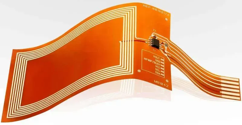
The foundation of any high-performance smart belt sensor PCB lies in the meticulous selection of its substrate material. This choice is paramount, directly influencing the device's flexibility, durability, signal integrity, and overall longevity, especially given the dynamic bending and environmental exposure inherent in wearable technology. For smart belts, the PCB must not only house intricate sensor arrays and processing units but also conform seamlessly to the human body, necessitating materials that can withstand repeated flexing without compromising electrical or mechanical performance.
| Material Type | Key Properties | Advantages for Smart Belt PCBs | Disadvantages for Smart Belt PCBs | Typical Applications |
|---|---|---|---|---|
| Polyimide (PI) - Flexible PCB (FPC) | Excellent flexibility, high temperature resistance, good electrical properties, lightweight | Conforms to body contours, high durability under repeated bending, ideal for compact designs | Higher cost than rigid PCBs, more complex manufacturing processes | Wearable electronics, medical devices, automotive flexible circuits |
| FR-4 (Rigid PCB) | High rigidity, good electrical insulation, cost-effective, widely available | Suitable for rigid sections or modules not requiring flexibility, robust component mounting | Lacks flexibility, prone to cracking under bending stress, not suitable for dynamic applications | General electronics, computers, power supplies (limited for smart belts) |
| Liquid Crystal Polymer (LCP) | Excellent flexibility, very low moisture absorption, high frequency performance, biocompatible | Superior moisture resistance for outdoor/sweat environments, good for high-speed signals | Very high cost, specialized processing required | Medical implants, high-frequency modules, aerospace |
| PEN (Polyethylene Naphthalate) | Good flexibility, better thermal stability than PET, lower cost than PI | Cost-effective flexible alternative, suitable for less demanding bending applications | Lower temperature resistance than PI, less robust for extreme bending cycles | Flexible displays, some flexible sensors, disposable medical devices |
Zero One Solution Limited excels in guiding clients through this critical material selection process, leveraging our deep understanding of the unique demands of smart belt sensor PCB solutions. Our expertise ensures that the chosen substrate not only meets the performance requirements but also aligns with cost targets and manufacturability constraints, leading to a robust, reliable, and market-ready product.
Effective sensor integration is paramount in smart belt sensor PCB solutions, directly influencing device accuracy, reliability, and user experience. Optimizing the placement of various sensors and establishing robust connectivity protocols are critical engineering challenges that, when mastered, unlock the full potential of these innovative wearables. Zero One Solution Limited specializes in advanced PCB layouts that strategically position sensors to mitigate noise and maximize data integrity, ensuring that critical health, fitness, or safety metrics are captured with unparalleled precision.
| Connectivity Protocol | Description | Advantages | Disadvantages | Typical Use Case | |||||
|---|---|---|---|---|---|---|---|---|---|
| I2C (Inter-Integrated Circuit) | A two-wire serial bus interface often used for short-distance communication between microcontrollers and peripherals. | Simple, low pin count, multi-master/multi-slave support. | Slower speed, limited address space, no built-in error checking. | Connecting multiple low-speed sensors (e.g., temperature, accelerometer). | |||||
| SPI (Serial Peripheral Interface) | A four-wire serial interface for synchronous data transfer between a master device and multiple slave devices. | High speed, full-duplex communication, no addressing overhead. | Higher pin count, no multi-master support, no standard acknowledgement. | Connecting high-speed sensors (e.g., IMUs, ADCs) and displays where speed is critical for real-time data flow in a Smart Belt Sensor PCB Solution for optimal performance of the sensor integration module providing a robust solution for a reliable connection. | UART (Universal Asynchronous Receiver-Transmitter) | A two-wire (Rx/Tx) serial communication protocol for asynchronous data transmission. | Simple, widely adopted, no clock signal needed. | Slower speed, no multi-master/multi-slave, requires careful baud rate matching. | Debugging, connecting GPS modules, or other serial communication peripherals. |
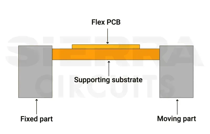
Designing flexible PCBs for smart belt sensors presents a unique set of engineering challenges, primarily centered around ensuring the circuit board can withstand repeated bending and torsional stresses without compromising electrical integrity or mechanical durability. Unlike rigid PCBs, flexible PCBs must be meticulously crafted to accommodate the dynamic movement inherent in wearable devices like smart belts, where continuous flexing is a core operational requirement. The goal is to achieve a design that is not only functional but also exceptionally reliable and long-lasting under real-world conditions.
| Design Aspect | Rigid PCB Approach | Flexible PCB Approach |
|---|---|---|
| Trace Bends | Often 90-degree sharp turns | Gentle arcs, tear-dropping, avoid sharp angles |
| Component Placement | Focus on electrical performance & density | Consider bend areas, minimize components in high-flex zones |
| Substrate Material | FR-4, high rigidity | Polyimide, Polyester (PET), high flexibility |
| Stress Management | Minimal consideration for bending | Extensive focus on strain relief, bend radius, layer structure |
| Copper Weight | Standard thicknesses | Often thinner copper for increased flexibility, or staggered layers |
The manufacturing process for Smart Belt Sensor PCBs is a meticulous journey from raw materials to a fully functional circuit board, demanding rigorous quality control at every stage to ensure the device's long-term reliability and performance. Unlike standard rigid PCBs, flexible PCBs for smart belts require specialized techniques to maintain integrity under constant bending and dynamic stress. This comprehensive approach encompasses precision fabrication, advanced component assembly, and exhaustive testing, all critical for delivering a robust and dependable Smart Belt Sensor PCB Solution that meets the stringent demands of wearable technology.
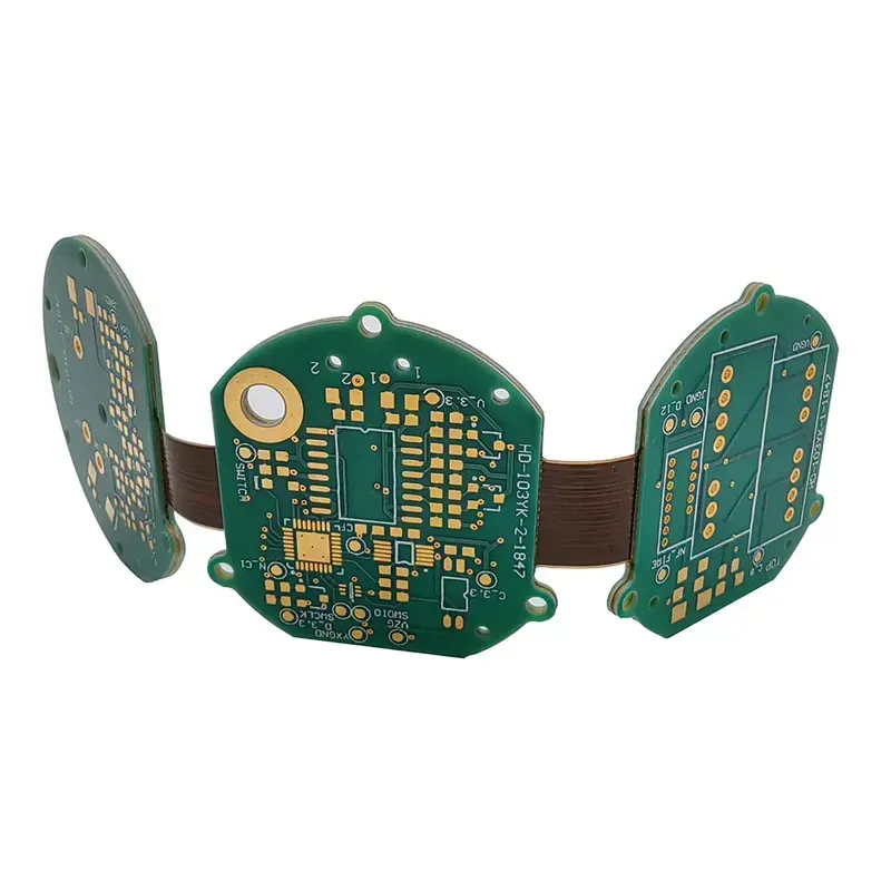
At Zero One Solution Limited, we are acutely aware that the success of innovative smart belt designs hinges on the underlying Printed Circuit Board (PCB) solution. Our deep expertise in rapid prototyping, precision manufacturing, and comprehensive assembly positions us as the indispensable partner for bringing your smart belt sensor concepts to life with unparalleled efficiency and reliability. We understand the unique demands of wearable technology, ensuring that every PCB we produce for smart belts is optimized for flexibility, durability, compact size, and seamless sensor integration.
| Capability Area | Specific Offering for Smart Belts | Benefit to Clients |
|---|---|---|
| PCB Design & Layout | Miniaturized, flexible/rigid-flex designs, optimized for sensor integration (e.g., IMUs, HR sensors) | Achieve compact form factors, high accuracy, and faster time-to-market |
| Rapid Prototyping | Quick-turn PCB fabrication and assembly for design validation | Accelerate R&D cycles, reduce development costs, and facilitate agile design iterations |
| Manufacturing (PCBA) | High-volume flexible PCB production, advanced SMT for fine-pitch components | Ensure robust, reliable, and scalable production with consistent quality |
| Quality Assurance | Rigorous testing protocols (AOI, X-ray, functional testing) specific to wearable PCBs | Guarantee long-term reliability and compliance with industry standards for consumer electronics |
Our commitment extends beyond just manufacturing; we provide strategic partnership, offering insights into material selection, component sourcing, and assembly techniques that specifically address the challenges of smart belt technology. With Zero One Solution Limited, you gain a partner dedicated to transforming your innovative smart belt concepts into market-ready products with efficiency and expertise.
At Zero One Solution Limited, our expertise in advanced PCB solutions has been instrumental in bringing numerous innovative smart belt products to market. These case studies highlight how our rapid prototyping capabilities, precision manufacturing, and comprehensive assembly services directly translate into enhanced product performance, superior reliability, and significantly accelerated time-to-market for our partners.
The smart belt market is rapidly evolving, driven by continuous innovation in sensor technology, wireless communication, and artificial intelligence. These advancements are not merely incremental; they represent a fundamental shift in how smart belts function and interact with users, demanding sophisticated PCB solutions that can accommodate these cutting-edge integrations while maintaining flexibility, durability, and compact form factors. Understanding these trends is crucial for staying at the forefront of smart belt PCB design and manufacturing.
In conclusion, the development of a smart belt sensor PCB requires a comprehensive understanding of material selection, sensor integration, flexible circuit design, and efficient manufacturing processes. Zero One Solution Limited stands as a leading provider of PCB solutions, offering rapid prototyping, expert design, and high-quality manufacturing services to empower our clients in the wearable technology market. We invite you to explore the possibilities of smart belt technology with Zero One Solution Limited. Contact us today to discuss your project and discover how our PCB solutions can accelerate your product development and bring your innovative ideas to life. Share this article with your colleagues and let's shape the future of wearable technology together!

