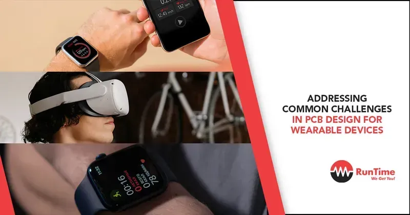
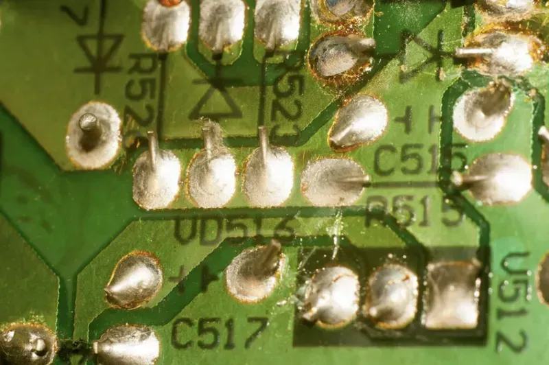
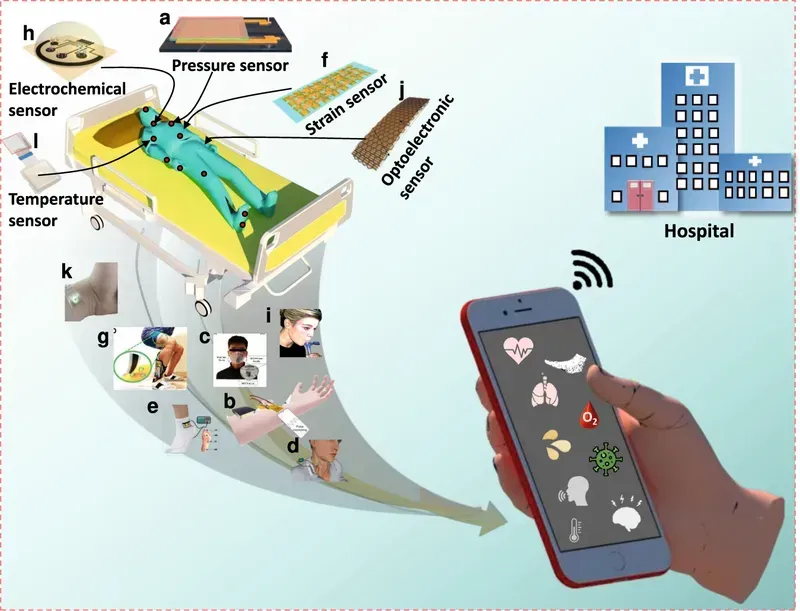
In today's rapidly evolving technological landscape, wearable devices are playing an increasingly critical role in various fields, from healthcare and fitness to environmental monitoring and industrial safety. At the heart of these devices lies the printed circuit board (PCB), the unsung hero responsible for connecting and supporting all the electronic components. Zero One Solution Limited, a leader in PCB solutions, offers specialized PCB solutions for wearable environment acquisition, empowering innovators to create cutting-edge devices. This article delves into the intricacies of wearable environment acquisition PCB solutions, highlighting their importance and showcasing Zero One Solution's expertise in this domain. What PCB design considerations are paramount when developing wearable environmental sensors? How does Zero One Solution ensure the reliability and performance of these miniature yet complex boards? Let's explore the world of wearable environment acquisition PCB solutions, uncovering the crucial role they play in enabling a new generation of smart, connected devices that enhance our understanding of the world around us.
Introduction to Wearable Environment Acquisition PCBs
Wearable Environment Acquisition PCBs (Printed Circuit Boards) are the foundational electronic platforms specifically engineered for compact, power-efficient integration of various sensors within wearable devices. These specialized PCBs are crucial for collecting real-time environmental data, enabling functionalities ranging from monitoring air quality and UV exposure to tracking temperature and humidity, thus transforming passive wearables into active environmental intelligence hubs. Their purpose is to miniaturize complex sensor arrays and processing units into a form factor suitable for body-worn applications, ensuring robust performance and user comfort.
What exactly is a Wearable Environment Acquisition PCB? A Wearable Environment Acquisition PCB is a compact, highly integrated circuit board designed to host a multitude of environmental sensors (e.g., temperature, humidity, air quality, UV, pressure) within a wearable device. Its core function is to facilitate the precise capture, processing, and transmission of real-time data from the wearer's surroundings, serving as the central nervous system for environmental sensing in smart wearables.
Why are specialized PCBs necessary for wearable environmental sensing? Specialized PCBs are critical due to the unique constraints of wearable technology. They must be ultra-compact, lightweight, flexible (in some applications), highly power-efficient to extend battery life, and resilient to physical stresses and environmental exposures. Standard PCBs often fail to meet these stringent requirements for size, power consumption, and durability in body-worn applications.
What kind of environmental data can these PCBs help acquire? Wearable Environment Acquisition PCBs can facilitate the acquisition of diverse environmental data. This includes but is not limited to: ambient temperature, relative humidity, atmospheric pressure, UV radiation levels, volatile organic compounds (VOCs), carbon monoxide (CO), carbon dioxide (CO2), and particulate matter (PM2.5/PM10) in the air. This data provides comprehensive insights into the wearer's immediate surroundings.
How do these PCBs contribute to the functionality of wearable devices? These PCBs are instrumental in transforming passive wearables into proactive environmental monitors. By integrating various sensors, they enable features such as personalized environmental alerts, data logging for long-term trend analysis, and real-time feedback on surrounding conditions. This enhances user safety, health, and overall awareness of their environment.
What are the primary challenges in designing Wearable Environment Acquisition PCBs? The primary challenges include achieving extreme miniaturization without compromising performance, managing power consumption to ensure long battery life, maintaining signal integrity despite tight component packing, ensuring robustness against physical impacts and moisture, and selecting biocompatible materials for direct skin contact. These factors demand highly specialized design and manufacturing expertise.
Key Design Considerations for Wearable Sensor PCBs
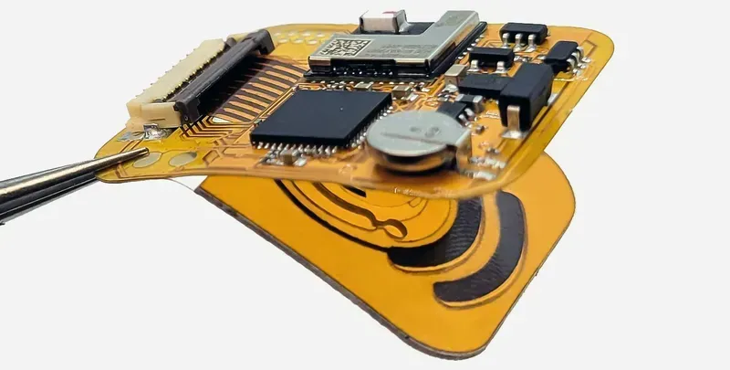
Wearable PCB Size Constraints
Designing Printed Circuit Boards (PCBs) for wearable environmental acquisition systems presents a unique set of challenges that demand meticulous attention to detail. Unlike traditional electronics, wearable PCBs must integrate seamlessly with the human body, enduring constant movement, varying temperatures, and potential exposure to moisture, all while maintaining precise functionality and minimal power consumption. Successfully navigating these considerations is paramount to developing reliable, efficient, and user-friendly wearable devices capable of accurate environmental sensing.
Design Consideration
Challenge
Impact on Wearable PCB Performance
Size and Form Factor
Miniaturization while integrating multiple components
Directly affects wearability, comfort, and aesthetic appeal; requires high-density interconnect (HDI) and compact component placement.
Power Efficiency
Extended battery life for continuous operation
Crucial for user convenience; necessitates low-power components, efficient power management ICs, and optimized circuit design to minimize current draw.
Signal Integrity
Maintaining data accuracy amidst noise and interference
Essential for reliable sensor readings; requires careful impedance matching, proper grounding, routing of sensitive traces, and EMI/EMC considerations.
Material Selection
Durability and flexibility for human-body interaction
Impacts longevity and comfort; demands materials resistant to bending, sweat, temperature extremes, and biocompatibility for skin contact (e.g., flexible PCBs, advanced substrates).
Thermal Management
Dissipating heat in confined spaces
Prevents component degradation and ensures user comfort; requires efficient heat dissipation strategies, especially for high-power components in enclosed designs.
Environmental Protection (IP Rating)
Resistance to moisture, dust, and sweat
Ensures operational reliability in various user environments; involves conformal coatings, robust enclosures, and sealed connectors to prevent ingress.
How does miniaturization impact wearable PCB design? Miniaturization in wearable PCB design is critical for achieving a compact form factor that is comfortable and unobtrusive for the user. It necessitates the use of advanced manufacturing techniques like High-Density Interconnect (HDI) technology, which allows for finer traces, smaller vias, and increased component density. This approach enables the integration of multiple sensors, processors, and communication modules into a minimal footprint without compromising performance, directly contributing to the device's aesthetic appeal and wearability.
Why is power efficiency so important for Wearable Sensor PCBs? Power efficiency is paramount for Wearable Sensor PCBs because it directly dictates the device's battery life and, consequently, user experience. Wearables are expected to operate continuously for extended periods without frequent recharging. Achieving high power efficiency involves selecting low-power consumption components, optimizing circuit designs to minimize leakage currents, implementing advanced power management integrated circuits (PMICs), and employing efficient communication protocols to conserve energy and prolong operational time between charges.
What are the key considerations for signal integrity in wearable environmental acquisition PCBs? Maintaining signal integrity in wearable environmental acquisition PCBs is vital for accurate and reliable data collection from sensitive sensors. Key considerations include careful impedance matching across transmission lines to prevent reflections, proper grounding schemes to minimize noise and crosstalk, and precise routing of analog and digital signals to avoid interference. Additionally, incorporating EMI/EMC shielding techniques is essential to protect sensitive sensor signals from external electromagnetic interference, ensuring the fidelity of acquired environmental data.
What materials are best suited for flexible wearable PCBs? For flexible wearable PCBs, materials such as Polyimide (PI) are highly favored due to their excellent flexibility, thermal stability, and mechanical strength. Other suitable materials include various types of liquid crystal polymer (LCP) and polyester (PET) films, which offer different degrees of flexibility, moisture resistance, and cost-effectiveness. The selection depends on the specific application's flexibility requirements, environmental exposure, and the need for biocompatibility, ensuring the PCB can withstand repeated bending and conform to the body's contours.
Environmental Sensors Commonly Integrated into Wearable PCBs
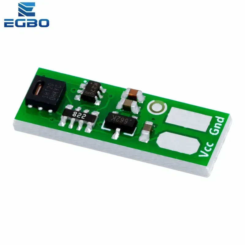
Temperature Humidity Sensor Wearable PCB
The efficacy of wearable environment acquisition solutions hinges on the precise integration of diverse environmental sensors into compact, high-performance PCBs. These miniature marvels enable wearables to gather critical data from their surroundings, transforming devices from simple trackers into sophisticated environmental monitors. The selection and integration of these sensors are paramount, directly impacting the device's accuracy, power consumption, and overall functionality in real-world scenarios. Leveraging advanced PCB design and manufacturing, Zero One Solution ensures seamless sensor integration, delivering robust and reliable wearable solutions capable of capturing a wide spectrum of environmental parameters.
Sensor Type
Key Environmental Parameter Measured
Typical Wearable Applications
Integration Considerations
Temperature Sensor
Ambient Temperature, Body Temperature
Smartwatches, Health Monitors, Industrial Safety Gear
Thermal management, minimal self-heating, high accuracy for medical applications
Humidity Sensor
Relative Humidity, Dew Point
Fitness Trackers, Climate Control Devices, Agricultural Wearables
Moisture resistance, stability over varied humidity levels, rapid response time
Wide dynamic range, minimal power consumption, interference immunity
Particulate Matter (PM) Sensor
PM2.5, PM10 Concentrations
Personal Air Purifiers, Urban Air Quality Monitoring Wearables
Miniaturization, low power, sensitivity to fine particles, filter integration
How does PCB design influence the performance of integrated environmental sensors in wearables? PCB design profoundly impacts sensor performance by dictating signal integrity, power delivery, and thermal management. A well-designed PCB minimizes noise, ensures stable voltage supply, and dissipates heat effectively, all crucial for sensor accuracy and longevity. Poor design can lead to signal degradation, inaccurate readings, and reduced sensor lifespan due to overheating or power fluctuations. Optimization involves careful trace routing, ground plane design, and component placement to prevent interference and ensure optimal operating conditions for each sensor.
At Zero One Solution, our deep understanding of these sensor integration nuances enables us to craft PCBs that unlock the full potential of wearable environmental acquisition systems, ensuring unparalleled performance and reliability.
Zero One Solution's Expertise in Wearable PCB Solutions
High Performance PCB Wearable Sensors
At Zero One Solution Limited, we bring over a decade of specialized expertise to the forefront of wearable environment acquisition PCB solutions. Our comprehensive capabilities span the entire lifecycle, from initial PCB design and meticulous manufacturing to high-precision assembly, all tailored to meet the rigorous demands of wearable environmental sensors. We understand that the future of wearable technology hinges on miniaturization, power efficiency, and robust performance, and our solutions are engineered to deliver precisely that, enabling our clients to innovate rapidly and effectively in this dynamic market.
Advanced Design & Engineering Our team of veteran engineers leverages state-of-the-art EDA tools and deep industry knowledge to craft highly optimized PCB layouts for wearable environmental sensors. We prioritize miniaturization, efficient signal routing, and thermal management to ensure optimal performance within confined spaces. Our designs are inherently robust, accounting for mechanical stresses and environmental exposures common in wearable applications.
Precision Manufacturing & Fabrication Zero One Solution boasts advanced manufacturing facilities in Shenzhen, enabling us to produce high-density, multi-layer PCBs with exceptional precision. We utilize cutting-edge fabrication techniques and adhere to stringent quality control protocols (e.g., IPC standards) to ensure every PCB meets the highest reliability and performance benchmarks. Our capabilities include fine-pitch component placement and complex HDI structures essential for compact wearable devices.
High-Performance Assembly (PCBA) Beyond manufacturing, our expertise extends to full PCBA services for wearable environmental sensors. Our assembly lines are equipped for handling miniature and sensitive components, including MEMS sensors and low-power ICs. We employ automated optical inspection (AOI) and X-ray inspection to guarantee solder joint integrity and component alignment, crucial for the long-term reliability of wearable devices operating in diverse environments. Our Dubai branch further extends our global reach and support.
Capability Area
Zero One Solution's Offering
Benefit for Wearable PCB Projects
Miniaturization & HDI
Advanced HDI (High-Density Interconnect) and microvia technology
Enables compact designs for smaller, more comfortable wearable devices
Power Management Optimization
Expertise in ultra-low power circuit design and component selection
Extends battery life, crucial for continuous environmental monitoring
Sensor Integration
Seamless integration of diverse environmental sensors (e.g., temperature, humidity, gas, UV)
Provides comprehensive environmental data acquisition capabilities
Material Selection
Access to advanced substrates (e.g., flexible, rigid-flex, specialized laminates)
Ensures durability and performance in challenging wearable environments
Rapid Prototyping
Fast-turnaround PCB fabrication and assembly services
Accelerates R&D cycles and reduces time-to-market for new wearable products
Rapid Prototyping for Accelerated Wearable Development
Wearable PCB Rapid Prototyping
In the fast-paced realm of wearable technology, rapid prototyping of PCBs is not merely an advantage; it is a critical enabler for innovation and market agility. Zero One Solution Limited specializes in delivering expedited PCB prototyping services, dramatically reducing the lead times from concept to functional wearable environmental sensing devices. This accelerated development cycle empowers our clients to rapidly test, iterate, and refine their designs, ensuring their products not only meet but exceed the demanding performance and integration requirements of the wearable market.
Design to Prototype in Record Time Zero One Solution leverages advanced manufacturing processes and an agile project management approach to compress the traditional prototyping timeline. Our integrated services, from PCB design optimization for wearables to efficient fabrication and assembly, mean clients receive working prototypes significantly faster than industry standards, typically within 3-5 business days for simple designs.
Iterative Development and Design Flexibility The ability to quickly produce multiple iterations is paramount for complex wearable designs that require fine-tuning of sensor placement, power management, and signal integrity. Our rapid prototyping capabilities facilitate a seamless iterative design process, allowing for real-world testing and immediate adjustments, thereby minimizing costly delays and ensuring optimal functionality before mass production.
Risk Mitigation and Cost Efficiency Early identification and resolution of design flaws through rapid prototyping significantly mitigate risks associated with product development. By detecting issues at an early stage, our clients avoid expensive rework or redesigns during later production phases, leading to substantial cost savings and a more predictable development trajectory for their wearable environment acquisition solutions.
Our commitment to rapid prototyping for wearable environment acquisition PCBs is a cornerstone of our value proposition, directly supporting our clients in accelerating their product launch cycles and maintaining a competitive edge.
Material Selection for Harsh Environments
PCB Material Exposed to Moisture
Selecting the optimal PCB materials is paramount for the long-term reliability and performance of wearable environment acquisition solutions, particularly when exposed to harsh environmental conditions such as extreme temperatures, high humidity, corrosive substances, or mechanical stress. The intrinsic properties of the chosen substrate, copper foil, and solder mask directly influence the device's resilience, signal integrity, and overall operational lifespan in challenging scenarios.
Material Type
Key Characteristics
Advantages for Harsh Environments
Disadvantages for Harsh Environments
FR-4
Standard fiberglass-reinforced epoxy laminate.
Cost-effective, widely available.
Limited moisture resistance, poor performance at extreme temperatures, susceptible to delamination under thermal cycling.
,High-Tg FR-4
Enhanced glass transition temperature FR-4.
Improved thermal stability, better resistance to delamination.
Still susceptible to moisture ingress, higher cost than standard FR-4.
,Polyimide
High-performance polymer, often used in flexible PCBs.
Excellent thermal stability, good chemical resistance, flexible.
Higher cost, can be challenging to process, moisture absorption can be a concern if not properly sealed.
,LCP (Liquid Crystal Polymer)
Thermoplastic polymer with excellent dielectric properties.
Very high cost, limited availability, specialized processing required.
,Ceramic Substrates (Alumina, Aluminum Nitride)
Inorganic, rigid materials.
Extremely high thermal conductivity, excellent dimensional stability, chemical resistance.
Brittle, very high cost, limited flexibility, heavy.
,Flexible Copper Clad Laminates (FCCL) with specialized adhesives
Polyimide or LCP films with copper layers and robust adhesives.
Enables conformal designs, excellent resistance to vibration and flex, can be combined with protective coatings.
Requires careful design for strain relief, material selection of adhesive is critical for long-term performance.
Zero One Solution Limited, leveraging its extensive experience in advanced PCB manufacturing, meticulously assesses environmental stress factors to recommend and utilize materials that guarantee the robustness and longevity of wearable environment acquisition PCBs. Our expertise extends beyond standard FR-4, incorporating specialized laminates and protective finishes that are crucial for devices operating in demanding conditions.
Ensuring Reliability and Longevity of Wearable PCBs
Ensuring the unwavering reliability and longevity of Wearable Environment Acquisition PCBs is paramount for continuous, accurate environmental data collection and user safety. The inherent challenges of wearable applications, including constant motion, varying environmental exposures, and power cycling, demand rigorous quality control and comprehensive testing protocols that extend far beyond standard PCB manufacturing, directly impacting the product's lifespan and performance in real-world scenarios. Zero One Solution Limited prioritizes a multi-faceted approach to achieve this critical objective.
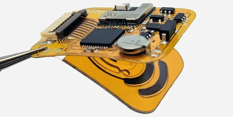
How does Zero One Solution ensure the durability of Wearable Environment Acquisition PCBs against constant movement and flexing? Zero One Solution employs advanced flexible and rigid-flex PCB technologies, utilizing substrates like polyimide (PI) that offer superior mechanical resilience. We incorporate sophisticated trace routing strategies to minimize stress points and utilize flexible interconnects. Furthermore, extensive mechanical stress testing, including repeated bending and torsion simulations, validates the design's ability to withstand the dynamic forces typical in wearable devices over their intended lifespan. Our IPC Class 2 and Class 3 manufacturing standards ensure robust solder joints and component attachment for long-term reliability under motion.
Reliability Measure
Description
Benefit for Wearable PCBs
Material Selection (Substrates)
Utilizing advanced substrates like high-Tg FR-4, polyimide (PI) for flexibility, and specialized low-Dk/Df materials for signal integrity.
Enhanced thermal stability, superior mechanical flexibility, and reduced signal loss crucial for miniaturized, high-performance wearable devices operating in diverse conditions.
Advanced Solder Paste & Process
Employing lead-free solder pastes with optimized reflow profiles, and advanced stencil printing for fine-pitch components.
Ensures robust, defect-free solder joints that resist thermal cycling and mechanical stress, critical for components in constantly moving wearable devices.
Automated Optical Inspection (AOI)
High-resolution optical inspection after solder paste application, component placement, and reflow to detect defects like shorts, opens, and missing components.
Early detection of manufacturing flaws, preventing failures down the line and ensuring the integrity of densely packed wearable circuits.
What specific tests are performed to validate the environmental resilience of these PCBs? Beyond standard functional testing, Zero One Solution subjects Wearable Environment Acquisition PCBs to accelerated life testing that simulates harsh operational conditions. This includes thermal cycling (rapid temperature changes), humidity testing (exposure to high moisture), salt spray testing (for corrosion resistance), and vibration/shock testing to replicate drops and impacts. These tests are conducted in environmental chambers to push the limits of the PCB's design and materials, ensuring they meet the stringent demands of real-world wearable applications.
Applications of Wearable Environment Acquisition PCBs
Wearable Environment Acquisition PCBs are pivotal in extending human perception, enabling compact, real-time data collection across diverse scenarios from personal health to industrial safety. Their ability to integrate sophisticated sensors into miniature, power-efficient form factors allows for unprecedented insights into the surrounding environment, driving innovation in fields demanding continuous, context-aware data.
Environmental Monitoring Wearable devices equipped with environmental acquisition PCBs are revolutionizing personal and localized environmental monitoring. They can track air quality (e.g., CO, NO2, VOCs), UV radiation, temperature, and humidity, providing individuals with real-time exposure data. This is crucial for outdoor enthusiasts, construction workers, or individuals with respiratory conditions, offering immediate alerts and long-term data for trend analysis. For instance, a wearable sensor could alert a cyclist to high ozone levels on their route or monitor a child's UV exposure during playtime, significantly enhancing personal safety and well-being. According to the EPA, personalized exposure monitoring is key to understanding true environmental impacts, and wearable PCBs are at the forefront of this capability.
Healthcare and Wellness In healthcare, these PCBs facilitate continuous patient monitoring beyond clinical settings. They enable devices that track vital signs in conjunction with ambient conditions, which can be critical for managing chronic diseases like asthma or cardiovascular issues. For example, a wearable might monitor a patient's heart rate and oxygen saturation while simultaneously detecting sudden changes in ambient pressure or temperature that could trigger symptoms. This integration provides a holistic view of the patient's physiological response to their environment. Furthermore, in rehabilitation, wearables can track activity levels and environmental factors impacting recovery, offering objective data for personalized treatment plans. The market for medical wearables is projected to grow significantly, underscoring the demand for such integrated solutions.
Fitness Tracking and Sports Performance Beyond basic activity tracking, wearable environment acquisition PCBs enhance fitness and sports performance analysis. Devices can monitor an athlete's physiological responses (e.g., sweat rate, core temperature) in relation to external factors like ambient temperature, humidity, and even altitude. This allows for optimized training regimens, preventing heatstroke during marathons or assessing performance efficiency in varying conditions. Coaches can gain deeper insights into how environmental stress impacts performance, leading to more targeted training and recovery strategies. Professional sports teams are increasingly adopting such technologies to gain a competitive edge and ensure athlete safety.
Industrial Safety and Worker Protection For industrial applications, these PCBs are vital for worker safety in hazardous environments. Wearable gas detectors, radiation sensors, and temperature monitors can alert workers to immediate dangers in factories, mines, or chemical plants. For instance, a wearable device could detect dangerous levels of carbon monoxide or methane before they become life-threatening, or monitor a worker's heat stress in extreme conditions. This proactive approach to safety can significantly reduce workplace accidents and occupational diseases. Companies are increasingly investing in smart PPE (Personal Protective Equipment) integrating these PCB solutions to ensure compliance with safety regulations and protect their workforce. The Occupational Safety and Health Administration (OSHA) emphasizes the importance of real-time monitoring for hazard control, making wearable environmental sensors indispensable.
Case Studies: Zero One Solution's Success Stories
Innovative Wearable Environmental Sensing Devices
Zero One Solution's commitment to innovation and precision engineering has led to numerous successful collaborations in the rapidly evolving wearable environment acquisition sector. Our expertise in navigating the complexities of miniaturization, power efficiency, and sensor integration has empowered clients to bring groundbreaking environmental sensing devices to market. These case studies underscore our capability to deliver robust, high-performance PCB solutions that meet stringent industry demands and push the boundaries of wearable technology.
Client Industry
Project Goal
Zero One Solution's Contribution
Key Outcome
Smart Agriculture
Develop a wearable sensor for hyper-local climate monitoring on crops.
Designed an ultra-low power PCB integrating temperature, humidity, and soil moisture sensors with BLE connectivity.
Reduced sensor package size by 30% and extended battery life by 50%, enabling continuous crop health monitoring for over 6 months on a single charge. Client achieved a 15% increase in yield due to optimized irrigation based on precise data.
Client Industry
Project Goal
Zero One Solution's Contribution
Key Outcome
Industrial Safety
Create a wearable gas detector for hazardous environments.
Developed a robust, explosion-proof PCB for toxic gas sensors (CO, H2S) with real-time data transmission and audible alarms.
Achieved IP68 rating and ATEX certification for the device, ensuring reliable operation in harsh industrial settings. The solution led to a 25% reduction in safety incidents related to gas exposure.
Client Industry
Project Goal
Zero One Solution's Contribution
Key Outcome
Personal Healthcare
Engineer a compact wearable device for continuous ambient UV exposure monitoring.
Designed a multi-layer rigid-flex PCB incorporating a miniature UV sensor, a low-power microcontroller, and a custom antenna for seamless data synchronization with a smartphone app.
Achieved a form factor small enough for discreet wearability, with less than 1% data packet loss, providing users with accurate, real-time UV index information and personalized sun protection recommendations.
Conclusion: The Future of Wearable Environmental Sensing
The convergence of miniaturization, advanced sensor technology, and robust PCB solutions is rapidly propelling wearable environmental sensing into a new era. Zero One Solution Limited stands at the forefront of this evolution, empowering innovators with the critical PCB foundation required to capture and analyze the world around us with unprecedented detail.
How do Zero One Solution's PCB advancements impact the future of wearable environmental sensing? Zero One Solution's commitment to rapid prototyping, stringent quality control, and specialized material selection directly accelerates product development cycles and enhances the reliability of wearable environmental sensing devices. This facilitates the integration of more sophisticated sensors and processing capabilities, leading to more accurate, real-time data acquisition and enabling new applications in health, safety, and smart environments.
What are the key benefits of partnering with Zero One Solution for wearable environmental sensing PCB solutions? Partnering with Zero One Solution offers several pivotal benefits, including access to deep expertise in miniaturized and power-efficient PCB design, rapid prototyping capabilities for quick iteration, stringent quality assurance processes ensuring reliability in diverse environments, and a global supply chain network for optimized material sourcing and production. This comprehensive support enables faster time-to-market and superior product performance for wearable environmental sensing devices.
In what emerging areas will wearable environmental sensing PCBs play a crucial role? Wearable environmental sensing PCBs will be instrumental in emerging areas such as personalized health monitoring for pollution exposure, smart city infrastructure for localized air quality assessment, advanced industrial safety wearables for real-time hazard detection, and nuanced athletic performance tracking incorporating environmental factors. Their ability to provide localized, real-time data will unlock unprecedented insights and drive innovation across multiple sectors.
How does Zero One Solution ensure the longevity of PCBs in harsh wearable environments? Zero One Solution ensures the longevity of PCBs in harsh wearable environments through a multi-faceted approach. This includes meticulous material selection, opting for substrates and coatings resistant to moisture, extreme temperatures, and chemical exposure. Furthermore, advanced design practices minimize stress points, while rigorous testing protocols, such as environmental chambers and accelerated life testing, validate durability under simulated real-world conditions.
What specific design considerations does Zero One Solution prioritize for high-performance wearable sensor integration? For high-performance wearable sensor integration, Zero One Solution prioritizes ultra-miniaturization, achieving high component density while maintaining signal integrity. Power efficiency is paramount to extend battery life, requiring optimized power management circuitry. Thermal management is also crucial to prevent overheating in compact designs. Finally, robust mechanical design ensures resilience against repeated flexing and external stresses common in wearable applications, all while maintaining excellent EMI/EMC performance for reliable data acquisition.
In conclusion, wearable environment acquisition PCB solutions are a cornerstone of modern technology, enabling a wide array of applications that enhance our understanding and interaction with the environment. Zero One Solution Limited stands at the forefront of this field, providing high-quality, reliable, and innovative PCB solutions tailored to the unique demands of wearable devices. By partnering with Zero One Solution, you gain access to expertise, rapid prototyping, and comprehensive support, empowering you to bring your wearable environmental sensing ideas to life.
Ready to revolutionize environmental monitoring with cutting-edge wearable technology? Contact Zero One Solution today to discuss your PCB needs and discover how our expertise can accelerate your product development journey. Let's collaborate to create a smarter, safer, and more connected world.