In today's fast-evolving tech landscape, smart bracelets have become more than just fitness trackers; they're sophisticated extensions of our digital lives. At the heart of every smart bracelet lies a complex Printed Circuit Board (PCB), the unsung hero responsible for its functionality. Imagine trying to fit the power of a smartphone onto your wrist – that’s the challenge PCB designers face. How do you miniaturize complex circuitry while ensuring reliability and performance? This article delves into the world of Smart Bracelet PCB Solutions, exploring the intricacies of design, manufacturing, and assembly, and highlighting how Zero One Solution Limited is leading the charge in this innovative field.
Understanding the Core of Smart Bracelet PCBs
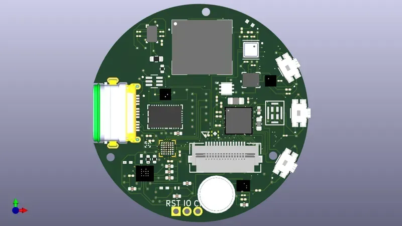
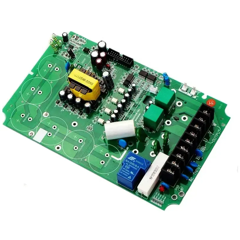
Smart bracelet PCB
At the heart of every smart bracelet, the Printed Circuit Board (PCB) serves as the foundational nervous system, intricately connecting and powering all its diverse functionalities. Far from being a mere component, the PCB dictates the device's capabilities, from precise health monitoring and seamless notification delivery to robust connectivity and extended battery life. Its compact yet complex design is paramount for integrating advanced sensors, processors, and communication modules into a wearable form factor, making it the critical enabler of the smart bracelet's performance and user experience.
What essential components are integrated onto a smart bracelet PCB? Smart bracelet PCBs integrate a miniaturized System-on-Chip (SoC) for processing, various sensors (e.g., optical heart rate, accelerometer, gyroscope, blood oxygen), power management ICs, Bluetooth/Wi-Fi modules for connectivity, flash memory for data storage, and charging circuitry, all meticulously arranged to optimize space and performance.
How does PCB design influence the battery life of a smart bracelet? PCB design significantly impacts battery life through efficient power management. Optimal component placement minimizes trace lengths, reducing signal loss and power consumption. The selection of low-power components, effective thermal dissipation strategies, and careful routing of power planes are crucial for maximizing energy efficiency and extending operational time between charges.
What role does the PCB play in enabling health tracking features? The PCB is central to health tracking, providing the physical platform for various biometric sensors (e.g., PPG for heart rate, SPO2 for blood oxygen) and their associated signal conditioning circuitry. It ensures stable power delivery and precise data transmission from these sensors to the SoC for processing, enabling accurate monitoring of vital signs, activity levels, and sleep patterns.
Why is miniaturization critical for smart bracelet PCBs? Miniaturization is critical for smart bracelet PCBs due to the inherent space constraints of wearable devices. A smaller PCB allows for a more compact and ergonomic device design, improving user comfort and aesthetics. This requires advanced manufacturing techniques like HDI (High-Density Interconnect) and precise component placement to pack maximum functionality into minimal space without compromising performance or reliability.
Key Functionality
PCB's Role in Enabling It
Design Implication
Health Monitoring
Hosts sensitive biosensors and analog-to-digital converters for accurate data capture.
Requires precise analog signal routing, noise suppression, and stable power delivery to sensors.
:Connectivity
Integrates Bluetooth, Wi-Fi, or NFC modules and their antennas for seamless communication.
Demands optimized RF trace routing, impedance control, and careful component isolation to prevent interference.
:User Interface
Connects display drivers, haptic feedback motors, and touch sensors for interactive experience.
Involves high-speed data lines for display, dedicated motor control circuits, and robust connections for physical inputs.
:Power Management
Manages battery charging, discharge, and voltage regulation for all components.
Incorporates efficient DC-DC converters, battery management ICs, and thermal considerations to prevent overheating and maximize battery life.
Design Considerations for Wearable PCBs
Designing printed circuit boards (PCBs) for smart bracelets presents a unique set of challenges that extend beyond conventional electronics. The intimate nature of wearables demands an acute focus on miniaturization, power efficiency, and mechanical flexibility. Successfully navigating these considerations is paramount to creating a device that is not only functional but also comfortable, durable, and appealing to the end-user, ultimately driving market adoption and user satisfaction. This section delves into the critical design factors that Zero One Solution Limited prioritizes to deliver optimal smart bracelet PCB solutions.
Miniaturization and Form Factor Smart bracelets require exceptionally small and thin PCBs to fit within compact enclosures without sacrificing aesthetic appeal or user comfort. This necessitates high-density interconnect (HDI) designs, fine-pitch component placement, and advanced routing strategies to maximize circuit density within minimal spatial constraints. Zero One Solution leverages advanced CAD tools and manufacturing processes to achieve these demanding miniaturization goals.
Power Efficiency and Battery Life Extended battery life is a key differentiator for wearable devices. PCB design plays a crucial role in achieving this through careful component selection (e.g., low-power microcontrollers, efficient power management ICs), optimized trace routing to minimize impedance and signal loss, and thoughtful power plane design to reduce noise and improve current distribution. Our designs prioritize efficiency to maximize device uptime.
Flexibility and Durability Wearable PCBs are often subjected to constant bending, twisting, and environmental stressors. This necessitates the use of flexible or rigid-flex PCB constructions that can withstand mechanical deformation without compromising electrical integrity. Material selection, stack-up configuration, and robust connection points are critical for ensuring long-term reliability and preventing fatigue failures under dynamic use conditions.
Signal Integrity and EMC/EMI Despite their small size, smart bracelet PCBs house sensitive analog and digital circuits operating at high frequencies. Maintaining signal integrity is vital for accurate sensor readings, reliable wireless communication (Bluetooth, NFC), and stable system performance. Furthermore, electromagnetic compatibility (EMC) and interference (EMI) mitigation are essential to prevent self-interference and ensure compliance with regulatory standards, which is achieved through careful grounding, shielding, and trace impedance control.
Thermal Management Heat dissipation in compact, enclosed wearable devices can be a significant challenge. Effective thermal management prevents component overheating, which can degrade performance and shorten device lifespan. PCB design contributes by strategically placing heat-generating components, utilizing thermal vias, and selecting materials with appropriate thermal conductivity, ensuring optimal operating temperatures for all integrated circuits.
Antenna Integration Seamless wireless connectivity is a cornerstone of smart bracelets. Integrating antennas directly onto the PCB or utilizing flexible antenna designs within the limited space is a critical design consideration. This requires expertise in RF design principles, impedance matching, and understanding the impact of surrounding materials on antenna performance to ensure reliable communication.
Material Selection: Choosing the Right Substrate for Smart Bracelet PCBs
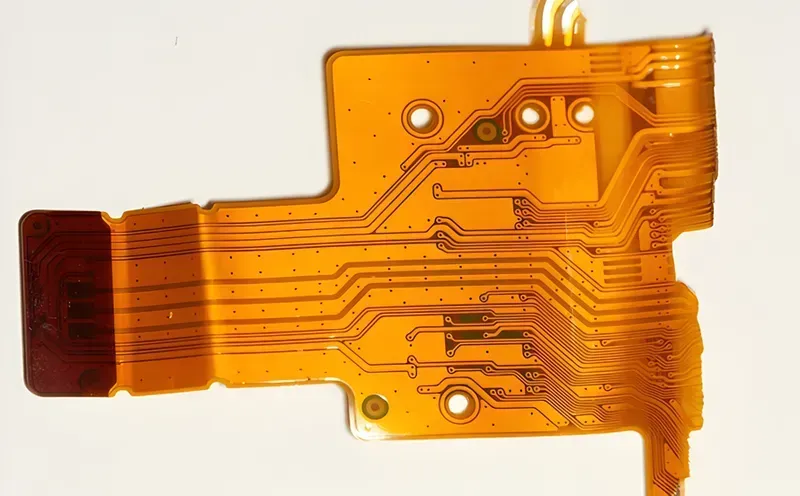
Kapton flexible substrate
The substrate is the foundational element of any Printed Circuit Board (PCB), and its selection for smart bracelets is paramount, directly influencing the device's durability, flexibility, thermal management, and signal integrity. Given the compact, often curved nature of wearables, traditional rigid FR-4 materials frequently fall short, necessitating a meticulous evaluation of advanced flexible and rigid-flex substrates. The ideal material ensures not only the physical resilience required for daily wear but also the electrical performance essential for sophisticated sensor integration and power efficiency.
Substrate Type
Advantages
Disadvantages
Typical Applications in Smart Bracelets
Flexible PCB (e.g., Polyimide/Kapton)
Exceptional flexibility and bendability; thin and lightweight; good thermal stability; ideal for dynamic bending applications.
Higher cost than rigid PCBs; lower dimensional stability compared to rigid boards; more complex manufacturing processes.
Cost-effective; widely available; good mechanical strength; well-understood manufacturing processes.
Rigid, not suitable for bending or conforming to irregular shapes; heavier and thicker than flexible alternatives.
Limited to specific, non-bending sections; primarily for control units where space allows and flexibility is not critical.
Why is material selection critical for smart bracelet PCBs? Material selection is critical because smart bracelets are subjected to constant movement, sweat, and varying temperatures. The chosen substrate must offer mechanical robustness against bending and impact, excellent thermal dissipation to prevent overheating of densely packed components, and stable electrical properties for reliable signal transmission, all while maintaining a slim and lightweight profile crucial for wearability.
What are the primary advantages of using flexible PCBs in smart bracelets? Flexible PCBs, often made from polyimide (Kapton), offer unparalleled design freedom, allowing the PCB to conform to curved surfaces or fit into highly constrained spaces. Their inherent flexibility enables devices to be lighter and thinner, improving user comfort and product aesthetics. They also facilitate dynamic bending, which is essential for components integrated into moving parts of a bracelet.
When would rigid-flex PCBs be preferred over purely flexible ones for a smart bracelet? Rigid-flex PCBs are preferred when a smart bracelet design requires both high component density, typically found on rigid boards, and flexible interconnections to navigate complex geometries or connect different modules. This hybrid approach provides enhanced reliability for solder joints on the rigid sections while maintaining the advantages of flexibility in other areas, making it ideal for compact designs with diverse functional blocks.
What specific properties of Kapton make it a popular choice for wearable PCBs? Kapton (polyimide) is highly favored for wearable PCBs due to its excellent dielectric strength, high thermal stability (withstanding high temperatures during manufacturing and operation), good chemical resistance, and superior mechanical properties, particularly its ability to withstand repeated bending without material degradation. Its thin profile also contributes significantly to miniaturization.
How does the selected PCB substrate impact the overall manufacturing process and cost? The substrate choice significantly impacts manufacturing complexity and cost. Flexible and rigid-flex materials generally require more specialized handling, processing equipment, and tighter tolerances during fabrication, leading to higher manufacturing costs and longer lead times compared to standard FR-4. However, the performance and design advantages often justify this increased investment for advanced smart bracelet functionalities.
Manufacturing Challenges and Solutions
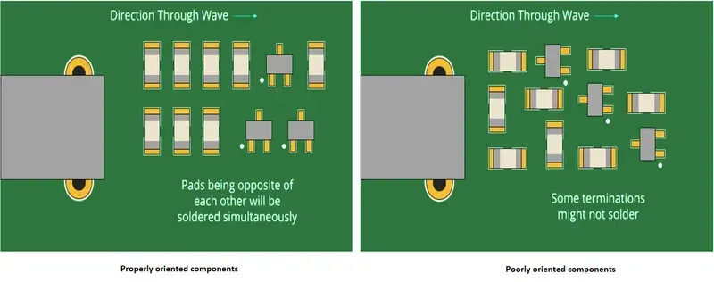
PCB component placement
Manufacturing miniature and flexible PCBs for smart bracelets presents unique challenges, primarily due to the stringent demands for compactness, durability, and intricate functionality. These hurdles necessitate advanced manufacturing techniques and rigorous process controls to ensure the high performance and reliability expected from wearable technology.
Component Placement Accuracy Challenge: The diminutive size of smart bracelet PCBs requires the placement of exceptionally small components (01005 and even 008004 packages) with extreme precision. Traditional pick-and-place machines may struggle with the tolerances, leading to misalignments or tombstoning.Solution: Utilizing high-precision, vision-guided automated pick-and-place equipment with sub-micron accuracy, coupled with advanced solder paste inspection (SPI) and automated optical inspection (AOI) systems, ensures accurate component placement and minimizes defects. Specialized nozzles and vacuum systems are also crucial.
Trace Routing Complexity and Signal Integrity Challenge: Densely packed circuits and the need for high-speed data transmission within a small footprint lead to complex trace routing. Ensuring signal integrity (minimizing crosstalk, impedance mismatches, and EMI) in such confined spaces is a significant hurdle.Solution: Employing multi-layer PCB designs (often 6-10 layers or more) and advanced routing software with design rule checking (DRC) and signal integrity analysis (SIA) capabilities is essential. Utilizing differential pairs, controlled impedance routing, and proper grounding techniques mitigates signal degradation. Furthermore, material selection with appropriate dielectric constants plays a vital role.
Thermal Management in Confined Spaces Challenge: Smart bracelets integrate powerful processors, communication modules, and sensors, all generating heat within a tiny, often enclosed space. Dissipating this heat effectively without compromising performance or user comfort is a complex manufacturing challenge.Solution: Incorporating thermal vias, copper pours, and specialized thermal pads into the PCB design. Strategic component placement to distribute heat, along with the use of thermally conductive materials in the PCB and enclosure, can improve heat dissipation. Simulation tools are used to predict thermal behavior and optimize designs.
Material Handling for Flexible and Rigid-Flex PCBs Challenge: Flexible and rigid-flex PCBs are delicate and prone to warping or damage during manufacturing processes like soldering, lamination, and handling. Maintaining dimensional stability and preventing delamination is critical.Solution: Implementing specialized fixtures and carriers designed for flexible substrates throughout the manufacturing process. Low-stress handling techniques, precise temperature control during reflow soldering, and vacuum lamination processes are crucial to prevent material deformation and ensure adhesion. Zero One Solution utilizes automated handling systems to minimize human error.
Assembly Techniques for High-Density PCBs
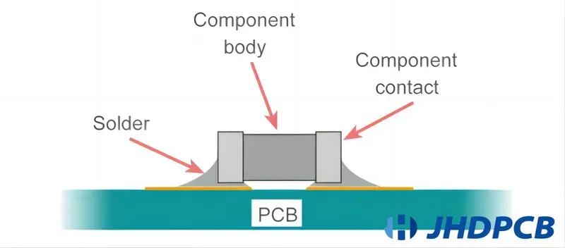
SMT Surface Mount Technology
Achieving the compact, feature-rich design of smart bracelets necessitates advanced PCB assembly techniques that can handle the extreme component density and miniaturization demands. Traditional assembly methods often fall short when dealing with the fine-pitch components and complex layouts inherent to wearable technology. Specialized approaches like Surface Mount Technology (SMT) and micro-BGA assembly are critical for precisely placing and soldering components, ensuring both electrical integrity and mechanical robustness within the limited real estate of a smart bracelet.
Surface Mount Technology (SMT) Optimization SMT is the cornerstone of high-density PCB assembly for smart bracelets. It involves mounting components directly onto the surface of the PCB, eliminating the need for through-holes. For smart bracelets, this means utilizing ultra-fine-pitch components (e.g., 0.3mm to 0.4mm pitch ICs), requiring highly precise pick-and-place machines, advanced solder paste printing with laser-cut stencils, and sophisticated reflow soldering profiles to prevent defects like bridging or tombstoning. The smaller component footprint and absence of drilling allow for greater component density and smaller board sizes, which are crucial for wearables.
Micro-BGA (Ball Grid Array) Assembly Micro-BGA packages are frequently used for processors, memory, and other complex integrated circuits in smart bracelets due to their high I/O density and small form factor. Assembling micro-BGAs, which have solder balls underneath the package, requires extremely tight process control. This includes precise solder paste deposition (often jetting or precise stencil printing), accurate component alignment using advanced vision systems, and optimized reflow profiles to ensure proper ball collapse and robust solder joints without voids or shorts. X-ray inspection is indispensable for verifying joint integrity as these connections are not visible externally.
ESD-safe handling, Grounding, Protective components on I/O lines
Testing and Quality Assurance of Smart Bracelet PCB Solutions
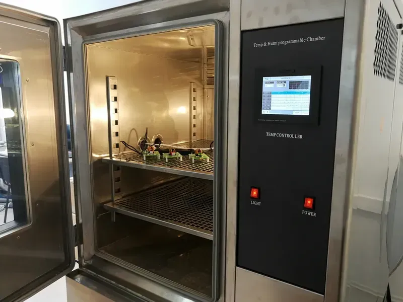
PCB environmental stress test
Ensuring the unwavering reliability and performance of Smart Bracelet PCB Solutions is paramount, given their continuous interaction with the user and diverse environmental conditions. Rigorous testing and comprehensive quality assurance protocols are not mere formalities but critical pillars that uphold the integrity and functionality of these compact, high-density circuits. Without exhaustive validation, even minor defects can lead to significant user dissatisfaction, product recalls, and reputational damage. Therefore, a multi-faceted approach to testing, encompassing everything from electrical verification to environmental resilience, is indispensable for delivering a robust and dependable smart wearable device.
Testing Procedure
Description
Key Focus Areas
Functional Testing
Verifies that the PCB performs all intended operations as per design specifications.
Connectivity, sensor readings (heart rate, accelerometer), display control, power management, wireless communication (Bluetooth/NFC).
Environmental Stress Testing (EST)
Subjects the PCB to extreme environmental conditions to assess its durability and performance limits.
Temperature cycling, humidity exposure, vibration, shock, ingress protection (IP) ratings for dust and water resistance, UV radiation effects (for exposed components).
Signal Integrity Analysis
Evaluates the quality of electrical signals on the PCB to ensure reliable data transmission and minimize errors.
Why is component-level testing crucial for Smart Bracelet PCBs? Component-level testing, often overlooked in the rush to market, is critical for Smart Bracelet PCBs due to their miniaturization and high component density. A single faulty micro-component can compromise the entire device's functionality. This testing verifies individual component performance against specifications before assembly, reducing costly rework and improving overall yield in high-volume production. It's about proactive defect detection rather than reactive troubleshooting.
What are the challenges of performing signal integrity analysis on flexible PCBs? Flexible PCBs, common in smart bracelets, introduce unique challenges for signal integrity. Their bendable nature can alter trace impedance, introduce unpredictable reflections, and increase crosstalk, especially at high frequencies. Maintaining consistent signal paths under dynamic conditions requires advanced simulation tools during design and specialized testing methodologies, such as TDR (Time Domain Reflectometry), to precisely characterize signal behavior across bends and flex points.
How does thermal testing contribute to the longevity of smart bracelets? Thermal testing is vital for the longevity of smart bracelets, which are often worn directly against the skin and house heat-generating components in confined spaces. Excessive heat can degrade component performance, shorten battery life, and even cause premature device failure. Thermal testing identifies hot spots, validates cooling mechanisms, and ensures the PCB operates reliably within its specified temperature range, preventing thermal runaway and extending the product's operational lifespan.
What role does X-ray inspection play in Smart Bracelet PCB quality assurance? X-ray inspection is an indispensable non-destructive testing method for Smart Bracelet PCBs, especially given their high-density interconnects and hidden solder joints (e.g., under BGAs, QFNs). It allows for the visual inspection of solder joint quality, voiding, component placement accuracy, and internal trace integrity, which are impossible to assess with optical inspection alone. This ensures robust physical connections crucial for device reliability and performance over time.
Why are automated optical inspection (AOI) and automated X-ray inspection (AXI) essential? For the intricate and high-volume production of Smart Bracelet PCBs, Automated Optical Inspection (AOI) and Automated X-ray Inspection (AXI) are essential for rapid, accurate, and consistent defect detection. AOI identifies surface defects like missing components, incorrect polarity, and solder bridging at high speeds, while AXI penetrates components to detect hidden solder joint defects. Together, they provide comprehensive coverage, significantly improving inspection throughput and reliability compared to manual methods.
Zero One Solution's Expertise in Smart Bracelet PCBs
Shenzhen PCB prototype
Zero One Solution Limited stands at the forefront of providing comprehensive PCB solutions specifically tailored for the demanding landscape of smart bracelet technology. Our deep-rooted expertise, cultivated since 2011, combined with our strategic global presence, empowers us to overcome the unique challenges of wearable electronics, ensuring rapid, reliable, and high-quality PCB manufacturing and assembly for your innovative products.
Rapid Prototyping for Accelerated Development We specialize in rapid-response R&D prototype manufacturing, enabling product developers to quickly iterate and validate their smart bracelet designs. Our agile approach significantly reduces time-to-market, turning concepts into tangible prototypes with exceptional efficiency. This rapid turnaround is crucial for competitive advantages in the fast-paced wearable tech market, allowing for early detection and resolution of design flaws.
One-Stop Solution from Design to Assembly Zero One Solution offers an end-to-end service for smart bracelet PCBs, encompassing everything from initial design consultation to manufacturing and final assembly. This integrated approach ensures seamless communication, optimized workflows, and superior quality control throughout the entire production lifecycle, eliminating the complexities of managing multiple vendors and streamlining the supply chain.
Service Aspect
Zero One Solution Advantage
Impact on Smart Bracelet Development
Miniaturization & High-Density PCBs
Advanced micro-BGA assembly and fine-pitch SMT capabilities; expertise in multi-layer flex/rigid-flex designs.
Enables sleek, compact smart bracelet designs with enhanced functionality and battery life, meeting aesthetic and performance demands of wearables.
Material & Component Sourcing
Global supply chain network with access to specialized flexible substrates and miniaturized components.
Ensures optimal material selection for durability, flexibility, and signal integrity, securing critical components for cutting-edge features.
Quality Assurance & Testing
Rigorous functional, environmental, and signal integrity testing protocols.
Guarantees robust and reliable performance in diverse user conditions, minimizing product recalls and enhancing brand reputation.
Geographic Advantage (Shenzhen & Dubai)
Headquartered in Shenzhen (electronic manufacturing hub) with a Dubai branch for global reach.
Facilitates efficient logistics, direct access to manufacturing innovations, and localized support for international clients, optimizing time and cost.
The Future of Wearable PCB Technology
The trajectory of Smart Bracelet PCB Solutions is marked by relentless innovation, driven by the demand for more advanced functionalities, prolonged battery life, and enhanced user comfort. As we look ahead, the future of wearable PCB technology will be defined by breakthroughs in materials science, manufacturing processes, and system integration, pushing the boundaries of what these compact devices can achieve.
Miniaturization Beyond Current Limits Future smart bracelet PCBs will achieve unprecedented levels of miniaturization through advanced manufacturing techniques like embedded component technology (ECT) and fan-out wafer-level packaging (FO-WLP). This will enable more features in smaller footprints, allowing for sleeker designs and less intrusive wearables. Research by Yole Développement projects a continuous shrinkage in package sizes for wearable electronics, driven by these innovations, leading to a projected 5-7% annual reduction in component size over the next five years, making devices virtually imperceptible on the wrist.
Advanced Sensor Integration and AI at the Edge The next generation of smart bracelet PCBs will integrate an even wider array of sophisticated sensors, including non-invasive glucose monitoring, advanced environmental sensors, and multi-modal biometric trackers. Furthermore, the incorporation of low-power AI accelerators directly onto the PCB will facilitate on-device data processing and machine learning, enabling real-time insights and proactive health management without constant reliance on cloud connectivity. This edge AI capability will reduce latency, improve data privacy, and significantly extend battery life.
Biocompatible and Stretchable Electronics Innovation in materials will lead to the widespread adoption of truly stretchable and biocompatible PCB substrates. These materials will not only conform seamlessly to the human body but also withstand extreme bending and torsion without compromising performance. This will unlock new possibilities for highly comfortable, skin-like wearables that offer continuous, unobtrusive monitoring, moving beyond current flexible PCB limitations to fully conformable and imperceptible devices. The development of stretchable conductive inks and polymers is key to this evolution, allowing for circuitry that moves with the skin.
Enhanced Power Solutions and Energy Harvesting Future smart bracelet PCBs will feature integrated power management units (PMUs) that are significantly more efficient, coupled with advancements in micro-batteries with higher energy densities. Beyond traditional batteries, there will be a greater emphasis on energy harvesting technologies directly integrated into the PCB, drawing power from body heat, kinetic movement, or even ambient RF signals, leading to devices that require minimal to no manual charging. This will be critical for always-on health monitoring and truly autonomous wearable experiences.
Modular and Customizable Architectures The future may see a shift towards more modular PCB designs for smart bracelets, allowing users or manufacturers to easily swap out or upgrade specific components like sensors or communication modules. This modularity could extend the lifespan of devices, reduce e-waste, and allow for greater personalization and specialization of functions, catering to diverse user needs and emerging applications. This approach will necessitate standardized interfaces and advanced inter-PCB connectivity solutions.
FAQs About Smart Bracelet PCB Solutions
What are the primary challenges in designing a Smart Bracelet PCB? The primary challenges in designing Smart Bracelet PCBs revolve around miniaturization, power efficiency, and flexibility. Achieving a compact form factor requires high-density interconnect (HDI) designs and advanced component packaging. Ensuring long battery life necessitates ultra-low power consumption circuits and efficient power management ICs. Furthermore, the wearable nature often demands flexible or rigid-flex PCB designs to conform to ergonomic requirements and withstand repeated bending without compromising integrity. These factors combined require a meticulous design approach from material selection to trace routing, balancing performance with physical constraints and reliability over time.
In conclusion, the Smart Bracelet PCB Solution is a multifaceted field that demands expertise, precision, and innovation. Zero One Solution Limited stands at the forefront, providing comprehensive services from design to assembly, ensuring that your wearable technology is not only functional but also reliable and market-ready. Whether you're developing a new fitness tracker or a sophisticated health monitoring device, partnering with a trusted PCB solution provider is paramount.
Ready to bring your smart bracelet vision to life? Contact Zero One Solution Limited today to discuss your PCB needs and discover how we can accelerate your product development cycle. Visit our website or reach out to our team in Shenzhen or Dubai to learn more.