In an era defined by escalating environmental concerns, the need for precise and reliable environmental monitoring has never been greater. Smart Environmental Sampling Stations stand as a crucial technological advancement in this field, enabling real-time data collection and analysis for a multitude of environmental parameters. At the heart of these sophisticated stations lies the Printed Circuit Board (PCB), the central nervous system that dictates functionality and reliability. Zero One Solution Limited, a leader in PCB solutions, offers comprehensive services from design to manufacturing and assembly, tailored specifically for smart environmental sampling stations. This article delves into the intricacies of PCB solutions for these stations, exploring the design considerations, manufacturing processes, and the critical role they play in ensuring accurate and dependable environmental monitoring.
Introduction to Smart Environmental Sampling Stations
Smart Environmental Sampling Stations are pivotal innovations revolutionizing modern environmental monitoring by providing automated, continuous, and precise data collection. These advanced systems transcend traditional manual sampling methods, offering unparalleled efficiency and accuracy in real-time ecological assessment. Their core utility lies in their ability to autonomously gather critical environmental parameters, enabling proactive responses to ecological shifts and informed decision-making for sustainable development. This section delves into the foundational aspects of these intelligent stations, highlighting their significance, the diverse parameters they monitor, and their broad spectrum of applications across various sectors.
What are Smart Environmental Sampling Stations? Smart Environmental Sampling Stations are automated, integrated systems designed for continuous, real-time monitoring of various environmental parameters. They typically comprise sensors, data acquisition modules, communication units, and a power source, all integrated onto a robust platform. These stations eliminate the need for manual sampling, providing consistent and reliable data streams essential for effective environmental management and research.
Why are these stations important for modern environmental monitoring? Their importance stems from the demand for timely, high-resolution environmental data. Unlike intermittent manual sampling, smart stations offer continuous monitoring, detecting subtle changes and rapid events that would otherwise be missed. This continuous data enables early warning systems for pollution, precise climate modeling, and more effective resource management, fundamentally enhancing our ability to understand and respond to environmental challenges.
What key parameters do Smart Environmental Sampling Stations typically measure? These stations are equipped to measure a wide array of environmental parameters depending on their specific application. Common measurements include air quality (e.g., PM2.5, PM10, CO, NO2, O3, SO2), water quality (e.g., pH, conductivity, dissolved oxygen, turbidity, temperature), meteorological data (e.g., temperature, humidity, wind speed/direction, barometric pressure, rainfall), and soil conditions (e.g., moisture, temperature, nutrient levels). Advanced stations may also monitor noise pollution or radiation levels.
What are the primary applications of Smart Environmental Sampling Stations? The applications are diverse and critical across multiple sectors. They are extensively used in urban air quality monitoring for public health, water resource management to assess purity and ecological health, agricultural optimization through soil condition analysis, industrial emission monitoring for regulatory compliance, and climate change research to track long-term trends. Furthermore, they are vital for disaster preparedness, providing real-time data during environmental emergencies like chemical spills or wildfires.
How do these stations contribute to sustainable development? By providing accurate, real-time environmental data, smart sampling stations empower stakeholders to make informed decisions that promote sustainability. This data facilitates the implementation of targeted environmental policies, optimizes resource allocation (e.g., water for irrigation), supports the development of renewable energy solutions, and enables adaptive management strategies for ecosystems, directly contributing to the United Nations Sustainable Development Goals related to clean water, air quality, and climate action.
The Critical Role of PCBs in Sampling Stations
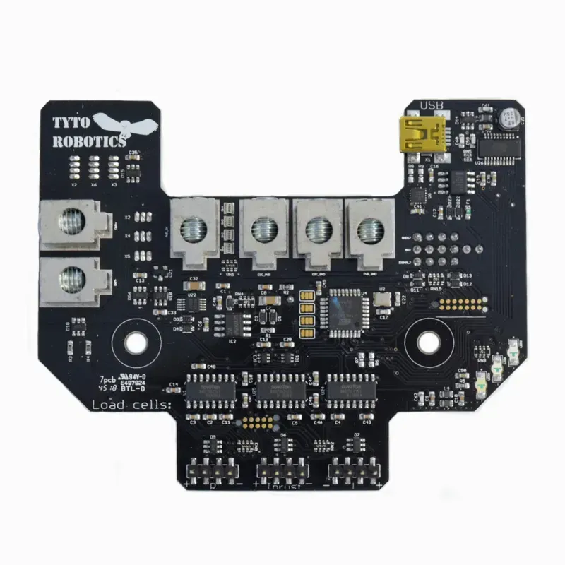
Environmental Sampling Station PCB Board
Printed Circuit Boards (PCBs) are the indispensable backbone of modern smart environmental sampling stations, serving as the central nervous system that orchestrates data acquisition, intelligent processing, and robust communication. Far from being mere electrical connectors, PCBs integrate diverse functionalities into a compact and resilient platform, enabling these stations to accurately monitor critical environmental parameters and transmit vital data efficiently, even in challenging remote locations. Their ability to consolidate complex electronic circuitry is paramount for the operational integrity and reliability of environmental monitoring infrastructure.
Data Acquisition Hub PCBs provide the foundational platform for integrating various environmental sensors (e.g., temperature, humidity, gas, particulate matter). They manage the precise analog-to-digital conversion of raw sensor data into actionable digital information, ensuring high fidelity and accuracy in measurements.
Signal Processing and Control At the core of the PCB, microcontrollers and digital signal processors (DSPs) are integrated to filter, analyze, and process the acquired data. This includes noise reduction, calibration adjustments, and executing programmed logic for automated sampling routines or real-time event detection.
Power Management Efficiency Environmental sampling stations often operate remotely with limited power sources (e.g., solar panels, batteries). PCBs are designed to incorporate sophisticated power management circuits that regulate voltage, optimize energy consumption, and ensure stable power delivery to all components, extending operational lifespan.
Communication Backbone For effective environmental monitoring, data must be reliably transmitted. PCBs integrate various communication modules (e.g., GSM/GPRS, LoRa, Wi-Fi, Ethernet) to facilitate secure and timely data transfer to central databases or cloud platforms for analysis and reporting.
Data Storage and Logging Many sampling stations require local data logging capabilities. PCBs accommodate non-volatile memory components (e.g., SD cards, flash memory) that store collected data, providing redundancy and ensuring no data loss even during communication interruptions or power outages.
Functionality Aspect
PCB Role in Smart Environmental Sampling Station
Sensor Integration
Provides stable electrical and mechanical interfaces for diverse sensors, ensuring accurate readings and minimal interference. Facilitates signal conditioning for optimal data acquisition.
Computational Core
Hosts the central processing unit (CPU) or microcontroller, enabling real-time data processing, algorithm execution, and decision-making directly at the sampling point.
Connectivity Management
Integrates wireless and wired communication modules, allowing seamless and secure data transmission to remote servers or monitoring centers through various protocols.
Durability & Reliability
Engineered with robust materials and layouts to withstand harsh environmental conditions, ensuring continuous operation and longevity of the sampling station.
Design Considerations for PCBs in Harsh Environments
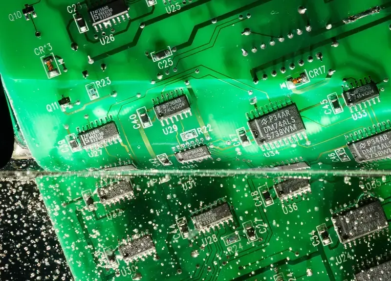
PCB Coating for Harsh Environments
Designing Printed Circuit Boards (PCBs) for smart environmental sampling stations presents unique challenges, primarily due to their exposure to harsh and unpredictable outdoor conditions. These environments demand a robust design philosophy, focusing on resilience against extreme temperature fluctuations, high humidity, corrosive elements, and mechanical stress. The integrity and longevity of the PCB directly impact the accuracy and reliability of the environmental data collected, making meticulous material selection and protective measures paramount for sustained operational performance.
Material Selection for Extreme Temperatures For PCBs operating in environments with significant temperature variations (e.g., -40
G to +85
G), materials with low Coefficient of Thermal Expansion (CTE) are crucial. FR-4, a common PCB substrate, can be optimized for higher Tg (glass transition temperature) to maintain dimensional stability. For more extreme conditions, specialized laminates like high-Tg epoxy or polyimide are employed, which offer superior thermal endurance and reduce the risk of delamination or warping under thermal cycling stress. IPC-2221 and IPC-4101 standards guide the selection of appropriate base materials for such applications, ensuring the PCB can withstand the specified temperature ranges without compromising functionality or structural integrity. Selecting materials that exhibit minimal expansion and contraction helps prevent stress on solder joints and component leads, which are common failure points in temperature-varying environments. Beyond the substrate, solder alloys with enhanced thermal cycling fatigue resistance, such as those containing bismuth or indium, can further improve reliability. Components themselves must also be rated for the intended temperature range, with industrial-grade or automotive-grade components often preferred for their wider operational specifications and proven robustness.
Mechanical reinforcement (staking, potting), robust component mounting, optimized board layout for stress distribution
Conformal Coatings for Enhanced Protection Conformal coatings are thin polymeric films applied to PCBs to protect electronic components from environmental stress. For harsh outdoor conditions, various types offer different advantages: Acrylic coatings (AR) provide good moisture resistance and are easy to rework. Urethane coatings (UR) offer excellent abrasion and chemical resistance. Silicone coatings (SR) are flexible, providing good vibration dampening and thermal shock resistance, ideal for extreme temperature cycling. Parylene coatings (XY) offer superior barrier properties, being pinhole-free and providing comprehensive protection against moisture, chemicals, and corrosive gases, though they are more expensive and require specialized vacuum deposition equipment. The choice of coating depends on the specific environmental threats and the required level of protection, with MIL-I-46058C and IPC-CC-830 standards guiding their application and performance. These coatings create a barrier that prevents moisture ingress, protects against chemical attack from pollutants, and mitigates the effects of condensation, which can lead to electrochemical migration and short circuits. Proper surface preparation before coating application is critical to ensure good adhesion and complete coverage, preventing potential pathways for contaminants.
Key Components and Functionality on the PCB
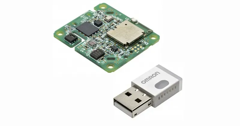
Environmental PCB Sensors
The Printed Circuit Board (PCB) serves as the central nervous system of a Smart Environmental Sampling Station, integrating various critical components that work in concert to accurately collect, process, and transmit environmental data. Understanding the interplay of these essential elements on the PCB is fundamental to designing a robust and reliable monitoring system capable of operating autonomously in challenging outdoor conditions.
Sensors and Analog-to-Digital Converters (ADCs) At the core of data acquisition are a variety of sensors (e.g., temperature, humidity, air quality, water quality, radiation, etc.) that convert physical parameters into analog electrical signals. These raw analog signals are then fed into Analog-to-Digital Converters (ADCs) on the PCB. The ADCs translate these continuous analog signals into discrete digital values, which are essential for processing by microcontrollers and digital data logging. High-resolution ADCs are crucial for ensuring the accuracy and precision of the collected environmental data.
Microcontroller Unit (MCU) The Microcontroller Unit (MCU) acts as the brain of the sampling station. It receives digital data from the ADCs, processes sensor readings, performs necessary calculations, and manages the overall system operation. The MCU controls data flow, executes algorithms for data validation and calibration, manages power consumption, and interfaces with other components like data loggers and communication modules. For environmental applications, MCUs with low power consumption and robust operating ranges are preferred.
Data Loggers and Memory Modules Environmental sampling stations often operate remotely, necessitating on-board data storage. Data loggers, typically comprising non-volatile memory modules (e.g., SD cards, eMMC, or Flash memory), are integrated onto the PCB to store collected data over extended periods. This ensures data integrity even if immediate transmission is not possible due to network unavailability or power fluctuations. The choice of memory depends on the volume of data, required read/write speeds, and environmental robustness.
Communication Modules For remote monitoring and data access, communication modules are vital components on the PCB. These modules enable the sampling station to transmit collected data to a central server or cloud platform. Common communication technologies include cellular (GSM/LTE), LoRaWAN, Wi-Fi, and Satellite communication, selected based on deployment location, data volume, and power constraints. The PCB design must accommodate the specific antenna requirements and power demands of these modules to ensure reliable connectivity.
Power Management Unit (PMU) Given that many environmental sampling stations are battery-powered and solar-charged, an efficient Power Management Unit (PMU) is indispensable. The PMU regulates power distribution to all components, optimizes energy consumption, manages battery charging, and provides power protection features. A well-designed PMU extends the operational lifespan of the station in remote environments, ensuring continuous monitoring without frequent human intervention.
Manufacturing Processes for High-Reliability PCBs
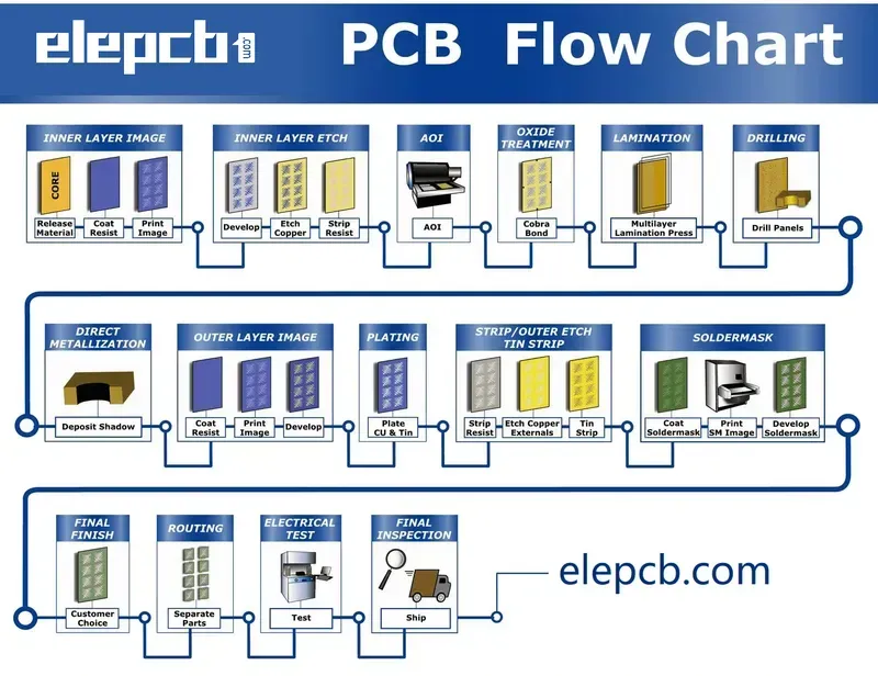
PCB Manufacturing Quality Control
The manufacturing of Printed Circuit Boards (PCBs) for smart environmental sampling stations demands a meticulous and stringent approach, as these devices operate in diverse and often challenging outdoor conditions. Achieving high reliability in such critical applications hinges on a comprehensive manufacturing process that prioritizes precision, quality control, and adherence to rigorous industry standards. This involves careful material selection, advanced fabrication techniques, and exhaustive testing protocols to ensure the PCB can withstand environmental stresses and deliver consistent performance over its operational lifespan.
Material Selection and Preparation The foundation of a reliable PCB lies in its materials. For environmental sampling stations, specialized substrates like high-Tg (glass transition temperature) laminates or ceramic-based materials are often chosen for their superior thermal stability and moisture resistance. Copper foil thickness is optimized for current handling and signal integrity. Surface finishes like ENIG (Electroless Nickel Immersion Gold) or Immersion Silver are preferred for their excellent solderability and corrosion resistance in harsh environments.
Precision Fabrication PCB fabrication involves precise etching to define circuit traces, drilling for vias and component holes, and multi-layer lamination to create complex board designs. Advanced techniques such as laser drilling for micro-vias and specialized etching processes are employed to achieve high-density interconnects (HDIs) and finer trace widths, crucial for integrating numerous sensors and communication modules. Controlled impedance routing is also critical for high-frequency signals from wireless communication modules.
Rigorous Quality Control and Inspection Throughout the manufacturing cycle, multiple stages of quality control are implemented. Automated Optical Inspection (AOI) systems are used after etching and drilling to detect defects like shorts, opens, and missing features. X-ray inspection is crucial for verifying internal layer alignment in multi-layer boards. Impedance testing ensures signal integrity, and solderability tests confirm the readiness of the board for assembly.
Protective Coatings and Encapsulation To further enhance reliability in environmental applications, protective coatings are applied. Conformal coating, a thin polymeric film, protects the PCB from moisture, dust, chemical contaminants, and temperature extremes. Potting or encapsulation provides a robust physical barrier against mechanical shock, vibration, and severe environmental ingress, crucial for long-term outdoor deployment.
Functional and Environmental Testing Before deployment, PCBs undergo extensive functional testing, including in-circuit testing (ICT) and boundary scan testing to verify component functionality and connections. Environmental stress screening (ESS) involves exposing the PCBs to simulated operational conditions, such as temperature cycling, humidity chambers, and vibration tests, to identify potential failure points and ensure robust performance under real-world stresses.
PCB Assembly and Integration Challenges
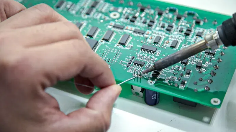
PCB Component Soldering
Integrating Printed Circuit Boards (PCBs) into smart environmental sampling stations presents a unique set of challenges, particularly given the harsh and unpredictable operational environments. Successfully navigating these complexities, from precise component placement to robust soldering and reliable interconnections, is critical to ensuring the long-term accuracy, stability, and longevity of the entire monitoring system. These challenges often stem from the need for high reliability in remote locations and the compact designs required for efficient deployment.
What are the primary challenges in PCB assembly for environmental sampling stations? The primary challenges include achieving precise component placement (especially for sensitive sensors), ensuring robust soldering to withstand vibrations and thermal cycles, managing thermal dissipation in sealed enclosures, maintaining signal integrity in noisy environments, and establishing reliable, weatherproof interconnections for external components and power sources. Miniaturization also adds complexity to fine-pitch component assembly.
Challenge Area
Description
Impact on Performance
Component Placement Accuracy
Precise alignment of fine-pitch components and sensors to ensure correct functionality and signal integrity.
Misalignment can lead to signal loss, short circuits, or incorrect sensor readings, compromising data accuracy and system reliability.
How does environmental exposure impact soldering techniques for these PCBs? Environmental exposure, particularly extreme temperature fluctuations and humidity, necessitates highly durable and reliable solder joints. Lead-free solder processes must be meticulously controlled to prevent brittle joints, and specialized flux chemistries may be required to ensure thorough wetting and minimize voids. Conformal coating application after soldering is crucial to protect against moisture and chemical ingress, preventing corrosion and short circuits.
Challenge Area
Description
Impact on Performance
Soldering Reliability
Ensuring strong, consistent solder joints that can withstand mechanical stress, thermal cycling, and vibrations without failure.
Weak or defective solder joints are a leading cause of intermittent failures, signal degradation, and complete system breakdown in the field.
What are the key considerations for ensuring proper electrical connections and signal integrity? Key considerations include using high-quality connectors designed for harsh environments (e.g., IP67 rated), employing proper shielding for sensitive signal lines to mitigate EMI/RFI, careful impedance matching, and robust cable management to prevent strain on connections. Grounding schemes must be meticulously designed to minimize noise and ensure stable operation of analog and digital circuits.
Challenge Area
Description
Impact on Performance
Interconnection Reliability
Establishing durable and weatherproof connections between the PCB and external sensors, power sources, and communication modules.
Poor interconnections can lead to intermittent power loss, data transmission errors, or complete system failure due to moisture ingress or mechanical stress.
What role does thermal management play in the assembly of these PCBs? Thermal management is critical, especially in sealed enclosures where active cooling is often not feasible. During assembly, components with high power dissipation must be strategically placed, and thermal interface materials (TIMs) or heat sinks may be integrated to dissipate heat effectively. Poor thermal management can lead to accelerated component degradation, performance issues, and premature system failure, particularly in extreme ambient temperatures.
Zero One Solution's Expertise in Environmental PCB Solutions
Zero One Solution Limited stands as a premier partner for the intricate demands of smart environmental sampling station PCB solutions. Our 13 years of specialized experience, rooted in Shenzhen's manufacturing prowess and extended globally through our Dubai branch, positions us uniquely to deliver robust, high-performance printed circuit boards that are indispensable for reliable environmental monitoring. We excel in transforming complex requirements into precise, durable PCB designs, leveraging our deep understanding of the unique challenges posed by harsh environmental conditions and the critical need for data integrity in such applications.
Why Choose Zero One Solution for Environmental PCB Needs? Zero One Solution offers a comprehensive, one-stop service from initial PCB design through manufacturing and assembly, specifically tailored for the high-reliability demands of environmental sampling stations. Our rapid prototyping capabilities significantly reduce development cycles, enabling faster time-to-market for innovative monitoring technologies. We combine Silicon Valley's innovative spirit with Shenzhen's manufacturing efficiency, ensuring both cutting-edge design and cost-effective production without compromising quality or performance.
Service Area
Zero One Solution's Core Competency
Benefit for Environmental PCB Solutions
PCB Design
Expertise in high-density, low-power designs resilient to environmental stressors.
Optimized performance and longevity in challenging outdoor deployments, ensuring accurate data capture and transmission.
Rapid Prototyping
Accelerated turnaround for R&D prototypes and pilot runs.
Enables quick iteration and validation of designs, significantly shortening product development timelines for new sampling station models.
Manufacturing & Assembly
ISO-certified processes, stringent quality control, and advanced assembly techniques.
Guarantees robust, reliable PCBs capable of enduring extreme temperatures, humidity, and corrosive agents, minimizing field failures and maintenance costs.
How does Zero One Solution ensure PCB reliability in extreme environmental conditions? We employ a rigorous multi-faceted approach, starting with material selection. We utilize substrates like high-Tg laminates and specialized coatings (e.g., conformal coatings) that resist moisture, chemicals, and extreme temperatures. Our design processes incorporate robust trace routing, thermal management, and EMI/EMC considerations. Furthermore, our manufacturing includes advanced soldering techniques and comprehensive testing, such as environmental stress screening (ESS) and functional testing, to ensure every PCB withstands the harshest outdoor conditions and delivers consistent performance over its lifecycle.
Case Studies: Successful PCB Implementations
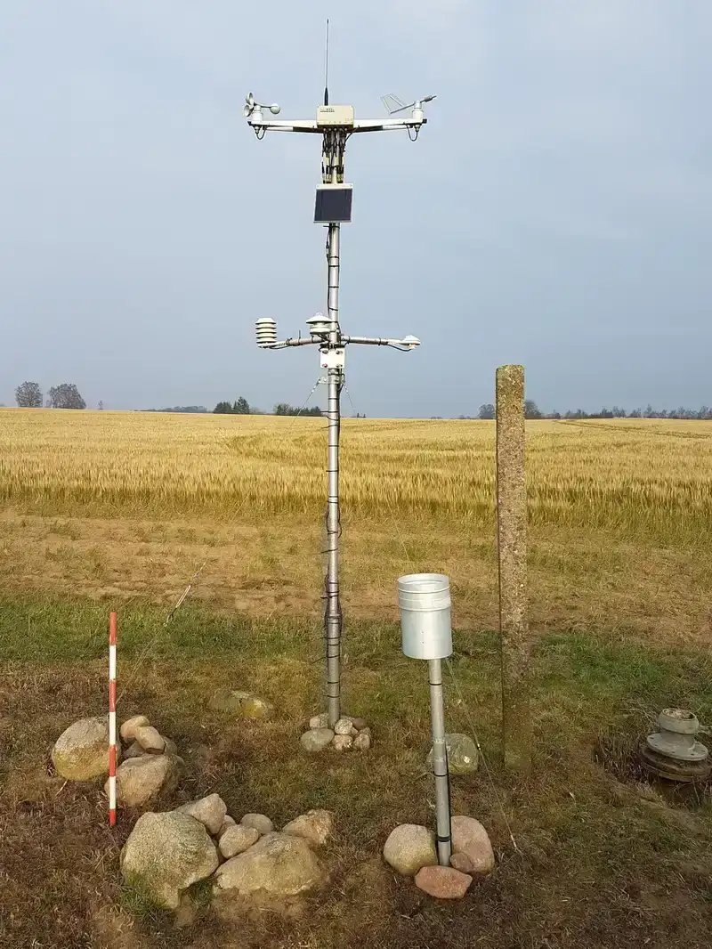
Environmental monitoring station onsite
Zero One Solution Limited's commitment to precision engineering and rapid prototyping has culminated in numerous successful implementations of PCB solutions for smart environmental sampling stations. Our expertise ensures that critical data acquisition, processing, and communication are seamless, even in the most demanding environmental conditions. These real-world applications underscore the robust reliability and superior performance of our custom-designed PCBs, directly addressing the complexities of accurate environmental monitoring.
Project Title
Key Challenge Addressed
Zero One Solution's PCB Solution
Outcome & Impact
Remote Air Quality Monitoring Network
Maintaining sensor accuracy and data transmission stability in extreme temperature fluctuations (-40°C to +85°C) and high humidity.
Developed a multi-layer PCB with conformal coating and industrial-grade components, featuring integrated temperature compensation circuitry and redundant communication modules.
Achieved 99.8% data transmission reliability and extended operational lifespan by 30% compared to previous solutions, enabling continuous, precise air quality assessments in remote areas. Reduced maintenance costs by 25%.
Coastal Water Quality Sentinel The challenge was to design a PCB that could withstand prolonged exposure to saltwater corrosion and maintain consistent performance for submersible sensors. Zero One Solution engineered a hermetically sealed PCB with specialized anti-corrosion finishes (ENIG) and marine-grade connectors, incorporating robust power management for long-term underwater deployment. The result was a 20% improvement in sensor data accuracy and a 50% reduction in field failures due to environmental ingress, ensuring reliable monitoring of marine ecosystems.
Future Trends in Environmental Monitoring and PCB Technology
The landscape of environmental monitoring is continuously evolving, driven by the imperative for more precise, real-time, and comprehensive data. This evolution is intrinsically linked to advancements in Printed Circuit Board (PCB) technology, which serves as the foundational enabler for next-generation smart environmental sampling stations. As a veteran SEO engineer and marketing expert, I emphasize that understanding these future trends in PCB technology is crucial for maintaining a competitive edge in the environmental monitoring sector, ensuring solutions are not only current but also future-proof.
Miniaturization and High-Density Interconnect (HDI) PCBs Future environmental sampling stations will demand significantly smaller footprints with increased functionality. This trend is driving the adoption of HDI PCBs, which allow for denser component placement and finer traces. By integrating more features into a compact form factor, these advanced PCBs facilitate the deployment of unobtrusive and highly scalable monitoring networks, enabling more pervasive data collection.
Advanced Wireless Communication Integration The push for real-time data transmission and remote accessibility will lead to more sophisticated wireless communication modules embedded directly onto PCBs. This includes enhanced support for LPWAN (Low Power Wide Area Network) technologies like LoRaWAN and NB-IoT, 5G, and even satellite communication for remote deployments. PCBs will need to manage higher data rates and more complex RF signal integrity requirements, necessitating advanced layout and material selection.
Enhanced Sensor Fusion and AI at the Edge Environmental monitoring is moving beyond single-parameter measurements to multi-sensor fusion, providing a holistic view of conditions. Future PCBs will integrate powerful microcontrollers or FPGAs capable of performing edge AI computations, enabling real-time data analysis, anomaly detection, and predictive modeling directly on the sampling station. This reduces data transmission bandwidth requirements and improves response times.
Energy Harvesting and Ultra-Low Power Designs To extend deployment lifetimes and reduce maintenance, future environmental sampling station PCBs will increasingly incorporate energy harvesting capabilities (e.g., solar, vibration, thermal) and employ ultra-low power design principles. This involves specialized power management ICs, optimized component selection, and innovative circuit layouts to minimize power consumption, allowing for prolonged operation in remote, unpowered locations.
Robustness and Self-Healing Capabilities As environmental sampling stations are deployed in increasingly harsh and diverse environments, PCBs will need enhanced resilience. This includes developing more robust coatings, hermetic sealing techniques, and even exploring self-healing materials or redundant circuit designs to ensure continuous operation despite physical or environmental stresses. The focus will be on maximizing uptime and minimizing field service interventions.
In conclusion, the PCB solution is the cornerstone of any smart environmental sampling station. Its design, manufacturing, and assembly directly impact the reliability and accuracy of environmental data collection. Zero One Solution Limited is dedicated to providing cutting-edge PCB solutions that meet the unique demands of these stations, enabling researchers, policymakers, and environmental agencies to make informed decisions based on trusted data. Contact us today to explore how our expertise can elevate your environmental monitoring capabilities. Zero One Solution: Your partner in a smarter, more sustainable future.