The smart grid represents a monumental leap in how we manage and distribute energy, promising increased efficiency, reliability, and sustainability. At the heart of this intelligent network lies the sensor node, the vigilant eyes and ears that gather crucial data, enabling informed decisions and optimized performance. But what is the key to unlocking the full potential of these sensor nodes? The answer lies in the Printed Circuit Board (PCB) solution that powers them. Zero One Solution Limited, a global leader in PCB solutions, offers cutting-edge smart grid sensor node PCB solutions designed to meet the demanding requirements of this critical application. This article will delve into the intricacies of smart grid sensor node PCB solutions, exploring their design considerations, manufacturing challenges, and the benefits they bring to the smart grid ecosystem.
Sensor nodes are the foundational intelligence of smart grids, acting as distributed data acquisition points that transform traditional power infrastructure into a dynamic, responsive network. These compact, interconnected devices are indispensable for real-time monitoring, enabling utilities to optimize energy distribution, enhance reliability, and integrate renewable sources efficiently. Their core function lies in gathering critical data points across the grid, facilitating predictive maintenance, fault detection, and precise load balancing, ultimately driving the smart grid's evolution towards a more resilient and sustainable energy future.
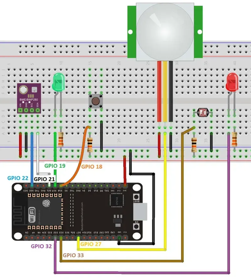
Designing Printed Circuit Boards (PCBs) for smart grid sensor nodes demands a meticulous approach, as these components are the bedrock of reliable energy distribution and monitoring. Optimal PCB design must balance intricate electrical requirements with the rugged demands of real-world deployment, ensuring signal integrity, robust power management, efficient thermal dissipation, and unwavering environmental resilience. These core considerations are paramount to achieving the long-term performance and reliability essential for critical infrastructure like the smart grid.
| Design Consideration | Impact on Smart Grid Sensor Node | Key PCB Design Approaches |
|---|---|---|
| Environmental Resilience | Ensures long-term operation in harsh outdoor or industrial settings (e.g., extreme temperatures, humidity, vibrations). | Selection of robust substrate materials (e.g., high Tg FR-4, polyimide), conformal coating application, robust enclosure design, vibration dampening techniques, and EMI/EMC shielding. |
void configure_sensor_node_power() {
    // Initialize power management unit
    PMU_init();

    // Set low-power modes for idle states
    PMU_set_sleep_mode(SENSOR_IDLE_MODE);

    // Configure voltage regulators for optimal efficiency
    REG_config_voltage(SENSOR_VOLTAGE_MAIN, REG_MODE_EFFICIENT);

    // Enable thermal monitoring to prevent overheating
    THERMAL_MONITOR_enable();

    // ... other power configuration ...
}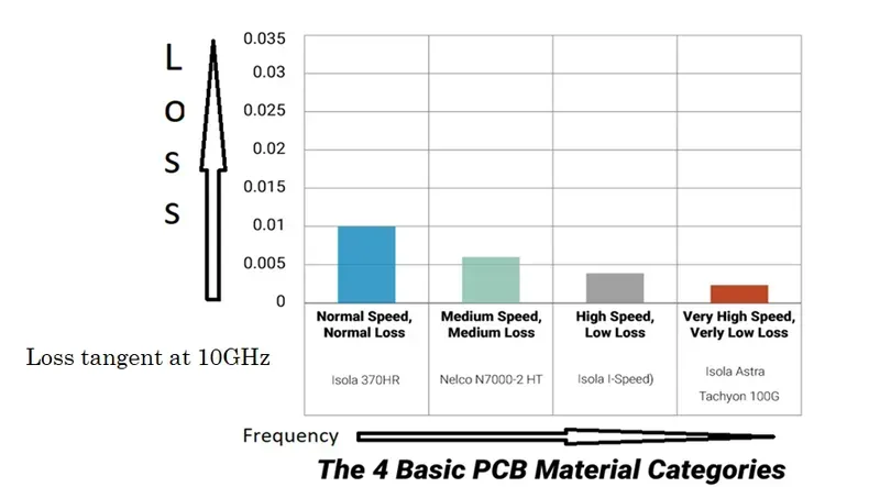
The operational integrity and longevity of Smart Grid Sensor Node PCBs are fundamentally dependent on the judicious selection of materials. These crucial components frequently operate in demanding environments, necessitating materials that exhibit exceptional resilience to extreme temperatures, voltage fluctuations, and harsh weather. The right material choice is not merely about functionality; it's about ensuring sustained reliability and optimal performance, minimizing downtime, and extending the lifespan of critical grid infrastructure. Prioritizing materials with high thermal conductivity and superior dielectric strength is paramount to mitigate risks associated with heat dissipation and electrical stress, ensuring the sensor nodes perform reliably over their extended service life.
| Material Property | Importance for Smart Grid PCBs | Recommended Characteristics |
|---|---|---|
| Thermal Conductivity | Dissipates heat from active components, preventing overheating and extending lifespan. | High (e.g., >0.8 W/m·K) to manage heat generated by power electronics and communication modules, especially in enclosed or high-ambient-temperature settings. Examples include Aluminum-backed laminates or copper-invar-copper (CIC) cores for improved heat spreading. |
| Material Property | Importance for Smart Grid PCBs | Recommended Characteristics |
|---|---|---|
| Dielectric Strength | Prevents electrical breakdown and ensures insulation integrity under varying voltage conditions. | High (e.g., >20 kV/mm) to withstand potential voltage spikes and maintain insulation effectiveness across power and signal layers, crucial for reliable data transmission and prevention of short circuits. Materials like High Tg FR-4 or Polyimide offer enhanced dielectric properties. |
| Material Property | Importance for Smart Grid PCBs | Recommended Characteristics |
|---|---|---|
| CTE (Coefficient of Thermal Expansion) | Matches expansion/contraction of components and solder, preventing stress and fatigue. | Low and matched to components (e.g., in the range of 10-18 ppm/°C for FR-4) to minimize stress on solder joints and vias during thermal cycling, which is common in outdoor or unconditioned smart grid deployments. Low CTE materials, especially those with ceramic fillers, help maintain structural integrity. |
| Material Property | Importance for Smart Grid PCBs | Recommended Characteristics |
|---|---|---|
| Moisture Absorption | Minimizes performance degradation and short circuits due to humidity. | Low (e.g., <0.1% for high-performance laminates) to prevent changes in dielectric constant, loss tangent, and potential delamination or shorting in humid or outdoor environments. Materials such as BT epoxy or specialized low-moisture-absorption resins are beneficial. |
| Material Property | Importance for Smart Grid PCBs | Recommended Characteristics |
|---|---|---|
| Flame Retardancy | Enhances safety and compliance with industry standards. | Meets UL 94 V-0 standard to ensure self-extinguishing properties in case of fire, critical for safety in grid infrastructure applications. Most modern PCB laminates, including various FR-4 types, satisfy this requirement. |
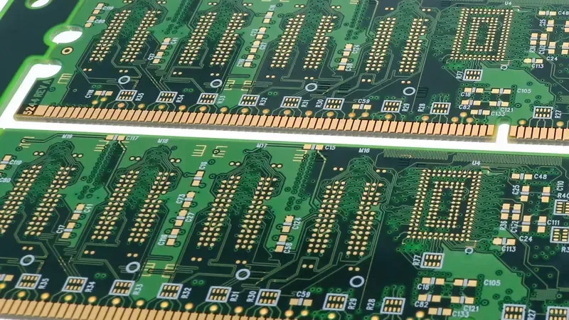
Manufacturing Printed Circuit Boards (PCBs) for smart grid sensor nodes presents a unique set of challenges due to their demanding operational environments and the critical need for long-term reliability. These PCBs are typically high-density and multi-layered, necessitating precise engineering and meticulous fabrication to ensure optimal performance over decades of continuous operation. Overcoming these manufacturing hurdles is paramount for the successful deployment and sustained functionality of smart grid infrastructure.
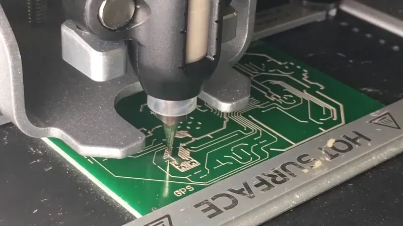
Rapid prototyping is an indispensable enabler for accelerating innovation in smart grid development, allowing engineers to quickly validate conceptual designs and iterate on improvements with unparalleled speed. In the complex landscape of smart grid sensor node PCBs, where intricate designs and stringent performance requirements are paramount, rapid prototyping significantly compresses the development cycle, transforming theoretical models into tangible, testable hardware. This agility is crucial for bringing cutting-edge smart grid solutions to market faster and more efficiently.
Zero One Solution Limited specializes in rapid-response R&D prototype manufacturing, offering comprehensive services that encompass PCB design, fabrication, and assembly. Our advanced capabilities and strategic location in Shenzhen, a global electronics manufacturing hub, ensure that your smart grid sensor node PCB prototypes are produced with exceptional speed and precision. We empower our clients to accelerate product development, validate innovative concepts swiftly, and achieve a significant reduction in their time-to-market, providing a crucial edge in the competitive smart grid industry.
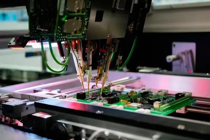
For Smart Grid Sensor Node PCB Solutions, meticulous PCB assembly and rigorous testing are paramount to guaranteeing the longevity and optimal performance of critical infrastructure components. The precision of assembly directly impacts signal integrity and power efficiency, while comprehensive testing validates functionality under various operating conditions, ensuring the reliability demanded by a resilient smart grid. Without these crucial steps, even the most robust PCB designs can falter, leading to system inefficiencies or failures.
| Assembly Process | Key Considerations for Smart Grid PCBs | Impact on Performance |
|---|---|---|
| Solder Paste Application | Precision alignment, controlled volume for fine-pitch components (e.g., microcontrollers, RF modules) | Ensures reliable electrical connections and prevents short circuits |
| Component Placement | Automated pick-and-place with high accuracy for dense layouts; proper orientation for polarity-sensitive components | Minimizes errors, optimizes signal paths, and enhances thermal dissipation |
| Reflow Soldering | Optimized thermal profile to prevent component damage and ensure robust solder joints across diverse material types | Guarantees strong mechanical and electrical connections, preventing cold solder joints or component stress |
| Rework and Repair | Controlled processes for component replacement, minimizing thermal stress on adjacent components and traces | Maintains PCB integrity and allows for efficient correction of defects without compromising board reliability |
| Testing Type | Description | Relevance for Smart Grid Sensor Node PCBs |
|---|---|---|
| In-Circuit Test (ICT) | Detects manufacturing defects such as shorts, opens, resistance, capacitance, and component presence/orientation. | Crucial for identifying early-stage assembly flaws, ensuring basic circuit integrity before functional testing, vital for complex multi-layer boards. |
| Functional Test (FCT) | Simulates the PCB's intended operating environment to verify its performance against design specifications. | Essential for validating sensor accuracy, communication protocols (e.g., Zigbee, LoRa), power management, and overall system response under various load conditions. |
| Environmental Stress Testing (EST) | Subjects the PCB to extreme temperature, humidity, and vibration cycles to identify potential failures under harsh conditions. | Indispensable for smart grid applications where sensor nodes are deployed outdoors or in challenging industrial environments, ensuring long-term reliability and durability. |
Zero One Solution Limited employs state-of-the-art assembly lines and advanced testing protocols, including automated optical inspection (AOI), X-ray inspection, and specialized functional test jigs. This ensures that every Smart Grid Sensor Node PCB delivered meets the highest standards of quality, reliability, and performance, contributing to the robustness and efficiency of modern smart grids.
Zero One Solution Limited stands at the forefront of providing comprehensive and reliable PCB solutions tailored specifically for the demanding requirements of smart grid sensor nodes. Our deep expertise, honed over a decade in the industry, ensures that our clients receive cutting-edge technology and unparalleled support from design inception to final assembly, empowering the next generation of energy infrastructure.
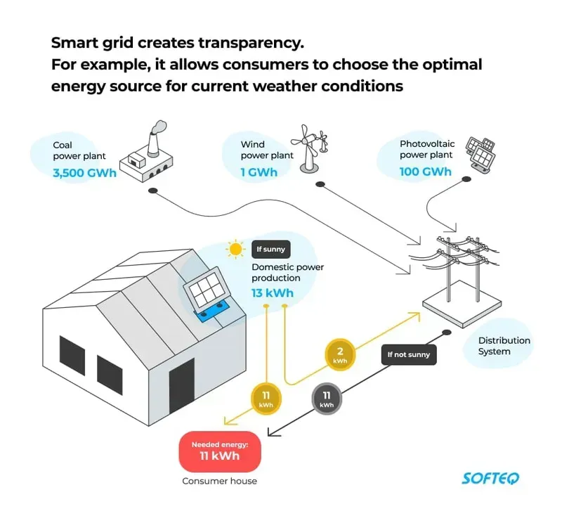
Real-world applications validate the profound impact of expertly engineered Smart Grid Sensor Node PCB Solutions. Zero One Solution Limited has a proven track record in collaborating with innovators to bring their smart grid visions to life, demonstrating tangible improvements in efficiency, reliability, and cost-effectiveness through our comprehensive PCB services. Our commitment to precision, speed, and quality is reflected in the successful deployment of advanced sensor nodes that underpin resilient and intelligent power infrastructure.
| Client | Challenge | Zero One Solution's Contribution | Key Outcome |
|---|---|---|---|
| Leading Utility Provider | Integrating renewable energy sources with existing grid infrastructure, requiring robust, high-precision sensor nodes for real-time data acquisition in diverse environmental conditions. | Provided rapid prototyping and manufacturing of multi-layer PCBs with advanced thermal management and EMI shielding for outdoor deployment. Utilized high-Tg materials for extreme temperature resilience. | 20% improvement in grid stability during peak renewable generation; 15% reduction in diagnostic time due to accurate sensor data. |
| Smart City Technology Firm | Developing compact, low-power sensor nodes for widespread urban deployment to monitor energy consumption and identify inefficiencies across commercial and residential sectors. | Designed and manufactured miniaturized, high-density PCBs with optimized power delivery networks (PDN) for extended battery life. Implemented stringent testing protocols for long-term reliability in urban settings. | Achieved 30% reduction in average energy consumption across monitored areas within 18 months; facilitated faster identification and resolution of energy leaks, saving significant operational costs. |
| Industrial IoT Innovator | Creating a distributed sensor network for critical infrastructure monitoring (e.g., substation equipment, transmission lines) requiring exceptional signal integrity and resilience to electromagnetic interference (EMI). | Engineered and produced specialized impedance-controlled PCBs with integrated ground planes and selective plating for superior signal integrity. Implemented advanced assembly techniques to ensure robust solder joints for high-vibration environments. | Increased predictive maintenance accuracy by 25%, leading to a 10% decrease in unexpected outages and a 5% reduction in overall maintenance costs through proactive issue resolution. |
Optimizing the reliability and longevity of Smart Grid Sensor Node PCBs is critical for the stability and efficiency of modern power distribution networks. These FAQs address common inquiries regarding their design, material selection, manufacturing, and testing, providing essential insights for robust smart grid deployments.
In conclusion, smart grid sensor node PCB solutions are a cornerstone of the modern smart grid, enabling real-time data acquisition, analysis, and control. Zero One Solution Limited stands at the forefront of this technology, offering comprehensive PCB solutions tailored to the unique needs of smart grid applications. From design and prototyping to manufacturing and assembly, we empower our clients to develop innovative and reliable smart grid solutions that drive efficiency, sustainability, and resilience. Contact Zero One Solution today to discuss your smart grid PCB requirements and discover how we can help you power the future of energy.

