In today's world, smart helmets are revolutionizing safety across various sectors, from construction and transportation to sports and emergency services. At the heart of every smart helmet lies a sophisticated printed circuit board (PCB), orchestrating the intricate dance of sensors, communication modules, and power management systems. Zero One Solution Limited understands the critical role these PCBs play and offers comprehensive Smart Helmet PCB solutions, empowering innovators to create cutting-edge head protection. How can a robust and reliable PCB design elevate the functionality and safety of smart helmets? This article delves into the world of Smart Helmet PCB solutions, exploring design considerations, manufacturing processes, and the crucial role Zero One Solution plays in bringing these life-saving technologies to market.
The evolution of traditional head protection into intelligent, connected devices marks a significant leap in safety, communication, and data acquisition across various sectors. Smart helmets, integral to this transformation, are increasingly indispensable in industries ranging from construction and mining to sports and healthcare. At their core, enabling the sophisticated functionalities of these devices are advanced Printed Circuit Boards (PCBs). These compact, robust, and highly integrated electronic components are the central nervous system, orchestrating everything from real-time impact detection and biometric monitoring to seamless wireless communication and environmental sensing. The burgeoning demand for these intelligent wearables directly correlates with the escalating need for highly specialized PCB solutions capable of withstanding harsh operational environments while delivering unparalleled performance and reliability.
| Industry Sector | Key Smart Helmet Features Enabled by PCB | PCB Requirement Emphasis |
|---|---|---|
| Construction & Industrial Safety | Impact detection, GPS tracking, Two-way communication, Environmental sensors (gas, temperature) | Robustness, Durability, Long battery life, EMI shielding |
| Sports & Recreation | Crash detection, Performance metrics (speed, G-force), Integrated audio, Live streaming capabilities | Miniaturization, Lightweight, High-frequency signal integrity, Water resistance |
| Healthcare & Rehabilitation | Fall detection, Vital sign monitoring, Telemedicine integration, Cognitive assessment | Precision sensing, Low power consumption, Biocompatibility, Data security |
| Emergency Services & Military | Night vision, Augmented reality overlays, Secure communication, Hazard detection | Extreme environmental resilience, High-speed data processing, Redundancy, Stealth features |
The increasing complexity of smart helmet functionalities, such as advanced sensor fusion for precise environmental mapping or integrated AI for predictive analytics, places unprecedented demands on PCB design and manufacturing. Miniaturization without compromising performance, efficient power management to extend operational battery life, and the ability to withstand extreme temperatures, vibrations, and moisture are paramount. Furthermore, seamless integration of multiple communication protocols (Bluetooth, Wi-Fi, cellular, UWB) and sophisticated data processing units requires meticulous PCB layout and material selection to ensure signal integrity and minimal electromagnetic interference (EMI). As smart helmets continue to evolve, the PCB remains the linchpin, driving innovation and expanding the boundaries of what these intelligent wearables can achieve.
Designing Printed Circuit Boards (PCBs) for smart helmets presents a unique set of engineering challenges that demand meticulous attention to detail. These challenges stem from the inherent need for compact, lightweight, highly reliable, and power-efficient electronics that can withstand demanding operational environments. Addressing these key design considerations from the outset is paramount to ensuring the functionality, safety, and market success of smart helmet solutions.
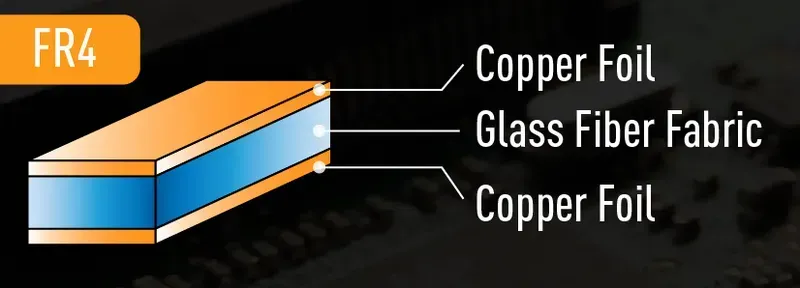
The robust performance and longevity of a smart helmet critically depend on the meticulous selection of its Printed Circuit Board (PCB) substrate materials. These materials must endure the harsh operational conditions inherent to smart helmets, including fluctuating temperatures, moisture exposure, and significant physical impacts, without compromising signal integrity or structural stability. Choosing the optimal substrate is paramount to ensuring the durability and high performance of smart helmet PCB solutions, directly influencing the device's reliability and user safety in diverse environments.
| Material Type | Key Characteristics | Advantages for Smart Helmets | Considerations/Limitations |
|---|---|---|---|
| FR-4 (Flame Retardant 4) | Rigid, cost-effective, good electrical properties, high glass transition temperature (Tg) | Good mechanical strength, widely available, suitable for core processing units | Less flexible, heavier, limited resistance to extreme impacts/flexing |
| Polyimide (Flexible PCBs) | High flexibility, excellent thermal stability, chemical resistance | Ideal for complex shapes and tight spaces, lightweight, excellent shock absorption | Higher cost, more complex manufacturing processes |
| High-Tg Materials (e.g., specific FR-4 variants) | Enhanced thermal resistance, stable performance at elevated temperatures | Reliable operation in high-heat environments (e.g., under direct sunlight or with heat-generating components) | Slightly higher cost than standard FR-4, can be more brittle |
| Hybrid Substrates (e.g., PTFE + FR-4) | Combines properties of different materials | Optimized for specific RF/high-speed applications while maintaining structural integrity | Higher complexity in design and manufacturing, increased cost |
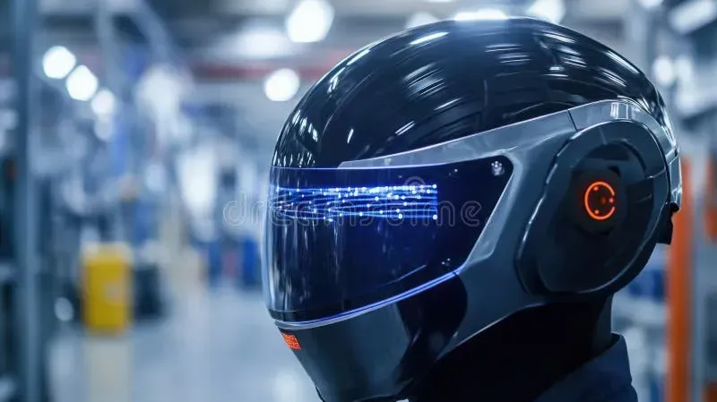
Optimizing space and functionality in Smart Helmet PCB solutions is paramount, given the constrained environment of a helmet. The integration of diverse components—sensors for impact detection and environmental monitoring, microcontrollers for data processing, communication modules like Bluetooth and Wi-Fi, and sophisticated power management circuits—requires a meticulous design approach. Efficient component placement and routing are critical to maximizing performance, minimizing electromagnetic interference (EMI), and ensuring the overall reliability and compact form factor essential for wearable technology. This involves not only selecting the smallest yet most powerful components but also employing advanced layout techniques to pack maximum functionality into minimal space without compromising signal integrity or thermal dissipation.
Zero One Solution Limited leverages its extensive experience in high-density interconnect (HDI) PCB design and manufacturing to tackle the complexities of smart helmet component integration. Our capabilities in micro-via technology and fine-pitch component assembly allow us to achieve unprecedented component densities while maintaining superior electrical performance and mechanical robustness, addressing the unique challenges of wearable electronics.
| Design Consideration | Impact on Smart Helmet PCB | Zero One Solution Approach |
|---|---|---|
| Space Constraints | Requires miniaturized components and high-density layouts. | Utilize HDI technology, SiP integration, and compact component libraries to maximize functionality in minimal space, achieving layouts as compact as 50mm x 30mm for core logic. |
function calculatePCBArea(components, spacing) {
  let totalArea = 0;
  for (let i = 0; i < components.length; i++) {
    totalArea += components[i].area;
  }
  return totalArea + (spacing * components.length);
}

// Example usage for a smart helmet PCB
const components = [
  { name: "MCU", area: 100 },
  { name: "Bluetooth Module", area: 50 },
  { name: "Accelerometer", area: 20 }
];
const spacingFactor = 5; // Minimal spacing between components
const estimatedArea = calculatePCBArea(components, spacingFactor);
// The actual layout optimization involves complex algorithms and design rules.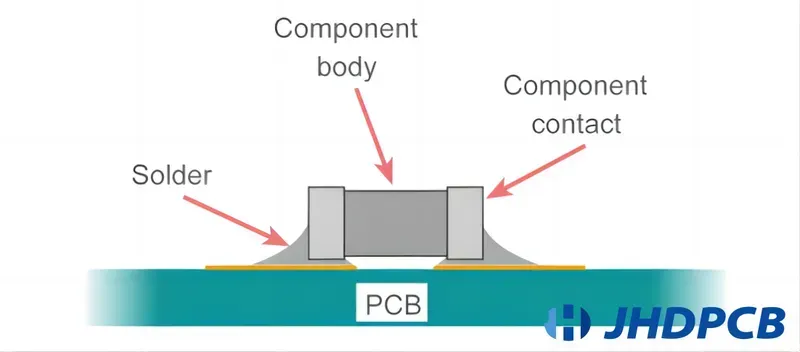
The manufacturing and assembly phase of Smart Helmet PCBs is paramount to ensuring the final product's reliability, durability, and ultimately, user safety. This stage transforms the meticulously designed layout into a functional circuit board capable of withstanding the rigorous demands of smart helmet applications. Precision engineering, stringent quality control, and adherence to established industry standards are not merely best practices but critical necessities in this specialized domain.
| Technology | Description | Application in Smart Helmet PCBs | Advantages | Disadvantages | |||||
|---|---|---|---|---|---|---|---|---|---|
| Surface Mount Technology (SMT) | Components are directly mounted onto the surface of the PCB. | Ideal for miniaturization and high-density component placement, crucial for compact smart helmet designs. | High component density, automated assembly, cost-effective for mass production. | Requires specialized equipment, challenges with large or odd-shaped components. | Through-Hole Technology (THT) | Components have leads that are inserted into drilled holes in the PCB and then soldered. | Used for robust connections, power components, or connectors requiring greater mechanical strength. | Stronger mechanical bond, easier for manual prototyping and repair, better for high-power applications. | Lower component density, slower assembly, higher drilling costs. |

For smart helmet PCBs, rigorous testing and validation are not merely a step in the production process but a fundamental imperative to ensure the device's reliability, performance, and, most critically, user safety. Given the demanding environments smart helmets operate in, from extreme temperatures to potential impacts, comprehensive validation procedures are essential to confirm that every integrated component and the overall PCB assembly function flawlessly under anticipated conditions, meeting both design specifications and stringent regulatory compliance standards worldwide.
Zero One Solution Limited stands at the forefront of providing comprehensive and cutting-edge PCB solutions specifically tailored for the demanding requirements of smart helmets. Our deep understanding of rapid prototyping, coupled with over a decade of industry experience, positions us as a trusted partner for innovators seeking to transform their smart helmet concepts into market-ready products. From initial design consultation to high-volume manufacturing and assembly, we ensure every Smart Helmet PCB Solution we deliver exemplifies precision, reliability, and superior performance, crucial for the safety and advanced functionality these devices promise.
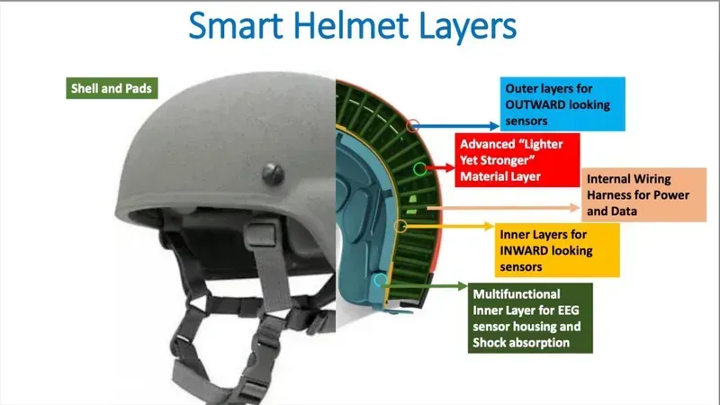
At Zero One Solution Limited, our extensive experience in rapid prototyping and high-quality PCB manufacturing has been instrumental in the development of numerous cutting-edge smart helmet projects. These case studies exemplify our commitment to overcoming complex engineering challenges, delivering robust and reliable PCB solutions, and ultimately accelerating our clients' time to market. We understand that each smart helmet application presents unique demands, and our tailored approach ensures optimal performance and seamless integration of advanced functionalities.
| Project Title | Challenge Addressed | Zero One Solution's Contribution | Key Benefit Achieved |
|---|---|---|---|
| Industrial Safety Helmet with Integrated Gas Detection | Miniaturization of sensor array and power management for hazardous environments. | Designed ultra-compact, multi-layer PCB with embedded gas sensors and custom power efficiency circuits; utilized flexible PCB for conformal fit. | Enhanced worker safety through real-time, accurate environmental monitoring in a lightweight form factor. |
| Motorcycle Smart Helmet with Advanced Communication | High-frequency signal integrity for Bluetooth/Wi-Fi, GPS, and audio processing within extreme vibration conditions. | Developed impedance-controlled PCB layouts, selected high-performance RF materials, and implemented vibration-resistant component placement and soldering techniques. | Superior audio clarity and uninterrupted connectivity for riders, even at high speeds and challenging terrain. |
| Sports Performance Tracking Helmet | Integration of multiple biometric sensors (EEG, heart rate) and a robust data logging module into a constrained, impact-resistant design. | Engineered a rigid-flex PCB to accommodate sensor placement and maintain structural integrity during impact, optimizing signal-to-noise ratio for accurate biometric data collection. | Provided athletes and coaches with precise, actionable performance insights without compromising helmet safety or comfort. |
| Emergency Responder Communication Helmet | Ensuring reliable, long-range communication and secure data transmission in harsh and unpredictable emergency scenarios. | Designed PCBs with enhanced EMI/EMC shielding, incorporated redundant communication pathways, and utilized ruggedized components for extreme temperature and moisture resistance. | Critical, uninterrupted communication for first responders, improving coordination and operational efficiency in life-saving situations. |
The evolution of smart helmets is intrinsically linked to advancements in their underlying PCB technology. As demand for more compact, powerful, and feature-rich smart helmets grows across sectors like sports, industrial safety, and defense, the PCBs driving them are undergoing significant transformations. These innovations are not merely incremental improvements but represent a paradigm shift towards highly integrated, flexible, and energy-efficient designs that will redefine the capabilities and adoption of smart helmet technology.
In summary, the Smart Helmet PCB solution is not just about assembling components; it's about creating a safe, reliable, and innovative product that can protect lives and enhance performance. Zero One Solution Limited is dedicated to providing comprehensive PCB solutions that meet the stringent demands of the smart helmet industry. By partnering with us, you gain access to our expertise in design, manufacturing, and assembly, ensuring your smart helmet project achieves optimal functionality and reliability. Contact us today to discuss your Smart Helmet PCB needs and discover how we can help you bring your vision to life. Whether you're developing a helmet for construction workers, athletes, or first responders, Zero One Solution is your trusted partner for PCB excellence.

