In today's interconnected world, the performance of network infrastructure hinges critically on the underlying hardware. At the heart of high-speed data communication lies the Switch Backplane PCB, a complex marvel of engineering that dictates data throughput, signal integrity, and system reliability. As a veteran engineer at Zero One Solution Limited, with two decades of experience in Silicon Valley's dynamic tech landscape, I've witnessed firsthand the evolution and increasing demands placed on these critical components. This article delves into the intricacies of Switch Backplane PCB solutions, highlighting how Zero One Solution Limited, a leader in rapid prototyping and one-stop PCB services since 2011, empowers clients to overcome the challenges of modern network design.
The Critical Role of Switch Backplane PCBs in Modern Networks
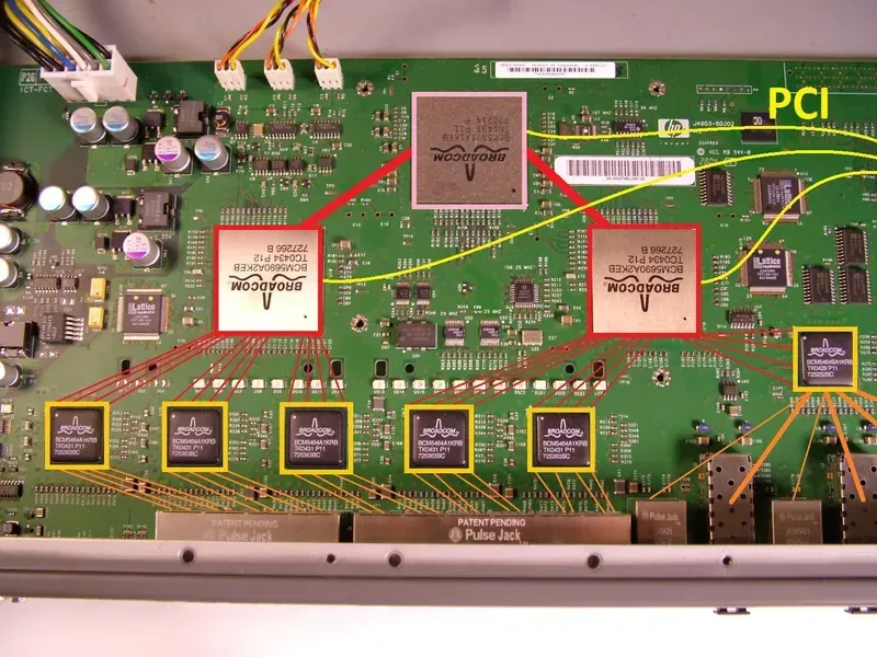
Switch Backplane PCB Close-Up
In the intricate architecture of modern communication networks, the Switch Backplane PCB serves as the undisputed central nervous system, orchestrating the seamless flow of high-speed data and ensuring robust system interconnection within switches and routers. This foundational component is far more than a mere circuit board; it is the critical conduit that dictates the performance, reliability, and scalability of network infrastructure. Without a meticulously designed and manufactured backplane, even the most advanced network processors and line cards would be rendered ineffective, making its role paramount in achieving the demanding data rates and low latency required by today's burgeoning digital landscape.
Core Functionality and Interconnection Hub The switch backplane PCB acts as the primary communication highway, connecting various functional modules such as line cards, power supply units, and control cards. It facilitates the rapid exchange of data packets and control signals between these components, eliminating the need for external cabling and significantly reducing signal path length, which is crucial for maintaining signal integrity at multi-gigabit speeds.
Enabling High-Speed Data Throughput Modern networks demand extraordinary data transfer rates, often reaching terabits per second. The backplane PCB is engineered to support these speeds through advanced material selection (e.g., low-loss laminates), precise impedance control, and sophisticated routing techniques. Its design directly impacts the system's ability to handle massive traffic volumes without bottlenecks or errors.
Power Delivery and Signal Integrity Beyond data transmission, the backplane is also responsible for distributing clean, stable power to all connected modules. A well-designed power delivery network (PDN) on the backplane is essential to minimize noise and voltage fluctuations, which can otherwise corrupt high-speed signals. The integration of robust power and signal planes ensures optimal performance and reliability for the entire system.
Scalability and Modular Design Switch backplanes are designed with modularity in mind, allowing for easy expansion and upgrades. This design principle enables network administrators to add or replace line cards as network demands evolve, extending the lifespan of the hardware and providing a cost-effective solution for future growth. The backplane's robust mechanical and electrical interfaces are key to this adaptability.
Key Challenges in Switch Backplane PCB Design
Designing switch backplane PCBs presents a confluence of formidable engineering challenges, demanding meticulous attention to various critical factors that directly impact system performance and reliability. These challenges are amplified by the relentless demand for higher data rates, increased port density, and reduced power consumption in modern network infrastructure. Overcoming these hurdles requires deep expertise in signal integrity, power integrity, thermal management, and robust mechanical design, ensuring the backplane can reliably serve as the high-speed data conduit and power distribution hub for complex networking equipment.
Signal Integrity (SI) Maintaining signal fidelity across high-speed interconnects is paramount. Challenges include minimizing crosstalk (unwanted coupling between adjacent traces), reducing reflection (signals bouncing back due to impedance mismatches), and mitigating jitter (variations in signal timing). Achieving this requires precise impedance control, careful trace routing, and advanced simulation techniques, especially with data rates exceeding 25 Gbps per lane, where even minor discontinuities can lead to significant data loss.
Power Integrity (PI) Delivering stable and clean power to numerous high-power components across a large board is critical. Challenges involve designing robust power delivery networks (PDNs) that minimize voltage droop, ground bounce, and power supply noise (PSN), which can corrupt high-speed signals. This necessitates optimizing plane capacitance, decoupling capacitor placement, and current distribution to ensure consistent voltage rails under dynamic load conditions.
Thermal Management High-density components and high-speed data flow generate significant heat. Effectively dissipating this heat is a major challenge, as elevated temperatures can degrade component performance, reduce reliability, and shorten lifespan. Design considerations include strategic component placement, optimizing copper distribution for heat spreading, and incorporating thermal vias and heat sinks to facilitate efficient heat transfer away from critical areas.
Mechanical and Material Considerations The sheer size and complexity of backplanes introduce mechanical challenges, including warpage, vibration resistance, and connector alignment. Selecting appropriate PCB materials with stable dielectric properties (low Dk and Df for high-speed signals) across varying temperatures and frequencies is crucial, as is ensuring robust lamination and stack-up construction to withstand mechanical stresses over the product's lifecycle.
Zero One Solution Limited's Expertise in High-Speed Backplane Design
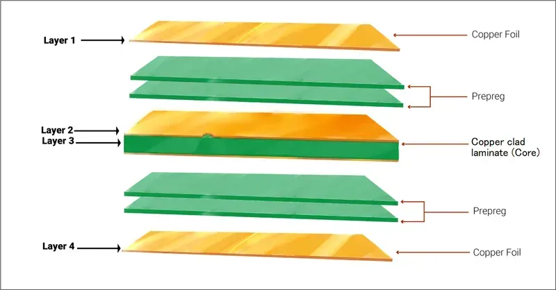
Multi-Layer PCB Stack-Up
Zero One Solution Limited stands at the forefront of high-speed backplane design, offering unparalleled expertise crucial for the performance and reliability of modern networking infrastructure. Our deep understanding of complex signal and power integrity challenges, combined with our proficiency in advanced manufacturing techniques, positions us as a leading partner in developing robust Switch Backplane PCB solutions. We leverage years of experience to transform intricate design specifications into high-performing, manufacturable PCBs, ensuring your networking products meet the stringent demands of data-intensive environments.
Multi-Layer Stack-Up Optimization Achieving optimal signal propagation and power delivery in high-speed backplanes necessitates meticulous multi-layer stack-up design. Zero One Solution Limited employs advanced simulation tools and iterative design processes to define precise layer arrangements, material dielectric constants, and copper thicknesses. This ensures controlled impedance, minimizes signal loss, and provides robust ground and power planes essential for high-frequency operation.
High-Density Interconnect (HDI) Implementation The increasing complexity and density of modern switches demand HDI technology for efficient component placement and signal routing. Our expertise in HDI includes microvias, staggered vias, and build-up layers, enabling finer line widths and spaces. This allows for superior routing density, reduced form factors, and enhanced electrical performance, critical for compact, high-throughput backplane designs.
Advanced Material Selection for Superior Performance The choice of PCB material is paramount for high-speed backplane performance. We guide clients through the selection of advanced laminates, considering factors such as dielectric loss (Df), dielectric constant (Dk) stability across frequencies, and thermal characteristics. Materials like low-loss FR-4, Megtron 6, or Nelco 4000-13 SI are strategically chosen to minimize signal attenuation, reduce dispersion, and ensure long-term reliability under demanding operating conditions.
Thermal Management Integration Effective thermal management is integral to the longevity and performance of high-speed backplanes. Our design approach incorporates thermal considerations from the outset, including strategic copper distribution, thermal vias, and integration with external cooling solutions. This mitigates heat buildup, preventing performance degradation and ensuring stable operation of high-power components.
Manufacturing Process Control for Reliability Beyond design, our expertise extends to controlling critical manufacturing processes that directly impact backplane reliability. This includes precise drilling, advanced plating techniques for robust vias, and stringent quality control during lamination and assembly. Our comprehensive process control ensures that the fabricated PCBs consistently meet the exact design specifications, delivering dependable performance.
Ensuring Signal Integrity (SI) in Switch Backplanes
Signal Integrity (SI) is paramount in Switch Backplane PCB solutions, directly influencing the reliability and performance of high-speed data transmission. In a complex network environment, even minor signal degradation can lead to significant data errors, reduced throughput, and system instability. At Zero One Solution Limited, our meticulous approach to SI ensures that critical data paths maintain their fidelity, minimizing phenomena such as crosstalk, reflection, and jitter. This proactive strategy is vital for achieving the high-bandwidth, low-latency communication demanded by modern switch architectures, safeguarding the integrity of every bit transmitted across the backplane.
Impedance Control Precise impedance matching is fundamental to preventing signal reflections. We employ advanced impedance calculation tools and controlled impedance routing techniques to ensure that transmission lines on the backplane maintain a consistent characteristic impedance (typically 50 Ohms differential, 100 Ohms single-ended) throughout the signal path, from driver to receiver. This includes careful selection of dielectric materials, trace width, and spacing.
Minimizing Crosstalk Crosstalk, the unwanted coupling of signals between adjacent traces, is a critical SI challenge in high-density backplanes. Our design methodologies include optimizing trace spacing, implementing differential routing where applicable, and utilizing guard traces or shielding techniques. We also employ strict layer stack-up definitions to provide sufficient isolation between high-speed signal layers and minimize inter-layer coupling.
Mitigating Reflection and Jitter Reflections occur when signals encounter impedance discontinuities, while jitter refers to variations in the timing of digital signals. To combat reflections, we focus on termination strategies (e.g., series, parallel, AC termination) and optimized via structures to reduce their impact. Jitter is addressed through careful clock distribution network design, power integrity optimization, and employing low-jitter clock sources, ensuring precise timing for high-speed interfaces.
Advanced Simulation and Validation Our SI assurance process is heavily reliant on state-of-the-art simulation tools. Before physical prototyping, we conduct extensive pre-layout and post-layout simulations, including S-parameter analysis, eye-diagram simulations, and TDR/TDT analysis. This allows us to predict and mitigate potential SI issues early in the design cycle, saving costly rework and accelerating time-to-market. Physical measurements and validation further confirm the simulation results.
Material Selection and Stack-Up Optimization The choice of PCB materials significantly impacts SI, especially at multi-gigabit speeds. We carefully select low-loss dielectric materials (e.g., Megtron 6, Isola I-Terra, etc.) with stable dielectric constants (Dk) and dissipation factors (Df) across frequency and temperature. Our multi-layer stack-up designs are meticulously optimized to provide optimal signal propagation, proper grounding, and efficient power distribution, crucial for maintaining signal integrity in dense backplane environments.
Achieving Power Integrity (PI) for Stable Operation
Achieving robust Power Integrity (PI) is paramount for the stable and reliable operation of high-speed switch backplane PCBs, as it directly impacts signal integrity and overall system performance. A well-designed Power Delivery Network (PDN) ensures a stable voltage supply, minimizes noise, and effectively handles dynamic current demands, which is crucial for the consistent operation of high-speed digital circuits. Without meticulous attention to PI, voltage fluctuations and ground bounce can lead to data errors, system instability, and even component damage, undermining the functionality of the entire switch infrastructure. At Zero One Solution Limited, we employ advanced methodologies and comprehensive analysis to design PDNs that meet the stringent requirements of modern backplane applications.
Why is Power Integrity (PI) critical for Switch Backplane PCB Solutions? Power Integrity is critical because it ensures a stable and noise-free power supply to all active components on the backplane. In high-speed switch environments, instantaneous current demands can fluctuate dramatically. Poor PI leads to voltage droop, ground bounce, and power supply noise, which directly degrade signal integrity, causing bit errors, reduced data rates, and system instability. A robust PDN ensures reliable data transmission and prevents premature component failure.
What are the key considerations in designing a robust Power Delivery Network (PDN) for Switch Backplane PCBs? Key considerations for PDN design include minimizing DC voltage drop, controlling AC impedance across a broad frequency range, and managing current density. This involves strategic placement of decoupling capacitors, optimizing power and ground plane geometries, selecting appropriate PCB materials with low dielectric loss, and designing power vias for minimal inductance. Additionally, considering the dynamic current draw of active components is vital to prevent transient voltage fluctuations.
How does Zero One Solution Limited ensure optimal Power Integrity in its Switch Backplane PCB designs? Zero One Solution Limited ensures optimal PI through a multi-faceted approach. We utilize advanced simulation tools for pre-layout and post-layout PI analysis, identifying potential voltage drops, current crowding, and resonant frequencies. Our design process includes optimizing power and ground plane distribution, implementing effective decoupling capacitor strategies, and utilizing low-inductance routing techniques. We also consider the thermal implications of current flow to maintain stable operating temperatures, ensuring long-term reliability.
What impact does poor Power Integrity have on the performance of a switch backplane? Poor Power Integrity can severely impact switch backplane performance. It can lead to increased bit error rates (BER) in high-speed data channels due to voltage fluctuations affecting signal thresholds. This can manifest as intermittent data loss, reduced system throughput, and even complete system crashes. It also contributes to increased electromagnetic interference (EMI) and makes the system more susceptible to external noise, ultimately compromising the overall reliability and longevity of the network equipment.
Are there specific materials or components that enhance Power Integrity in Switch Backplane PCBs? Yes, specific materials and components significantly enhance PI. Low-ESL (Equivalent Series Inductance) and low-ESR (Equivalent Series Resistance) decoupling capacitors are crucial for effective noise suppression. High-dielectric-constant materials for embedded capacitance can improve power delivery. For the PCB substrate, materials with stable dielectric properties and low loss tangents minimize power dissipation. Additionally, copper foil thickness and layer stack-up are optimized to reduce resistance and inductance, directly impacting PDN efficiency.
Rapid Prototyping and Manufacturing for Accelerated Development
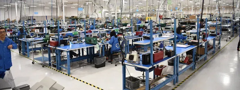
PCB Prototype Manufacturing Workshop
In the fast-paced world of network infrastructure, the ability to rapidly prototype and manufacture Switch Backplane PCBs is not merely a convenience but a critical competitive advantage. Zero One Solution Limited excels in providing accelerated R&D prototype manufacturing, enabling our clients to swiftly iterate, test, and validate their intricate backplane designs. This rapid-response capability significantly shortens product development cycles, allowing innovations to move from concept to market at an unprecedented pace, directly impacting time-to-market and overall project success.
How does rapid prototyping benefit Switch Backplane PCB development? Rapid prototyping for Switch Backplane PCBs allows for quick design iteration and validation, significantly reducing time-to-market. It enables engineers to identify and rectify design flaws early, mitigate risks, and optimize performance before committing to mass production. This iterative approach fosters innovation and ensures a more robust and reliable final product.
Comprehensive One-Stop Service: From Design to Assembly
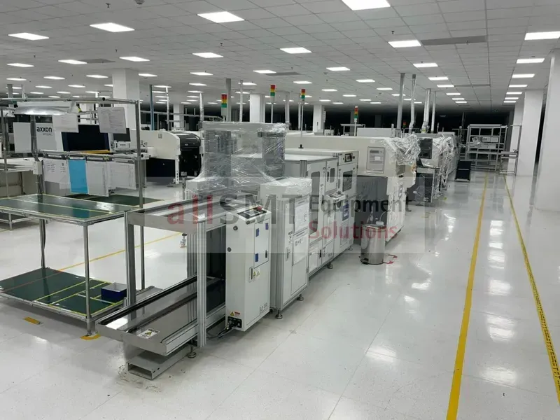
PCB Assembly Production Line
At Zero One Solution Limited, our comprehensive one-stop service for Switch Backplane PCB solutions transcends traditional engagements by offering seamless integration from initial design concepts to final assembly. This holistic approach significantly streamlines the product development cycle, mitigating risks and accelerating time-to-market for complex networking hardware. By consolidating the entire process under one roof, we eliminate the complexities of managing multiple vendors, ensuring consistent quality, superior communication, and optimized efficiency throughout every stage of your project.
Integrated Design & Engineering Our expert engineers collaborate closely with your team from the conceptualization phase, employing advanced DFM (Design for Manufacturability) and DFA (Design for Assembly) principles. This proactive integration ensures that design choices optimize both performance and production efficiency, addressing potential challenges before they impact timelines or costs. We leverage cutting-edge simulation tools to validate designs for signal integrity, power integrity, and thermal performance.
High-Precision PCB Manufacturing With state-of-the-art facilities, we specialize in manufacturing high-layer count, high-density interconnect (HDI) Switch Backplane PCBs. Our manufacturing processes adhere to stringent quality controls, utilizing a diverse range of advanced materials to meet the demanding requirements of high-speed data transmission and robust mechanical integrity. We ensure tight tolerances, reliable impedance control, and exceptional panel utilization.
Advanced Assembly & Testing Our assembly services encompass advanced surface mount technology (SMT), through-hole technology (THT), and precise BGA/LGA placements for complex components often found on backplanes. Post-assembly, comprehensive testing, including ICT (In-Circuit Test), functional testing, and environmental stress screening, validates the performance and reliability of the assembled Switch Backplane PCBs, guaranteeing they meet your exact specifications and industry standards.
Global Reach and Supply Chain Advantage
Global PCBA Supply Chain Map
Zero One Solution Limited's strategic global presence, anchored by our headquarters in Shenzhen, China's electronic manufacturing hub, and a key branch office in Dubai, provides an unparalleled advantage in delivering advanced Switch Backplane PCB solutions. This dual-location strategy ensures not only efficient project execution but also seamless access to a robust global PCBA supply chain, critical for rapid prototyping and large-scale manufacturing of complex backplane designs.
Shenzhen: The Global Electronics Epicenter Our headquarters in Shenzhen grants us direct access to the world's most comprehensive and agile electronics manufacturing ecosystem. This allows for optimized material sourcing, advanced fabrication capabilities, and swift turnaround times for high-density, multi-layer Switch Backplane PCBs, crucial for meeting stringent market demands. Leveraging this proximity to innovation and production streamlines our operational efficiency and cost-effectiveness for our clients.
Dubai: Bridging East and West The Dubai branch office strategically positions Zero One Solution Limited as a pivotal link between Asian manufacturing prowess and Western market demands. This hub facilitates efficient logistics, strengthens client relationships across diverse regions, and provides localized support, ensuring a responsive and reliable partnership regardless of geographical location. It enhances our ability to navigate international trade and supply chain complexities seamlessly.
Advantage Category
Impact of Shenzhen Base
Impact of Dubai Branch
Supply Chain Access
Direct access to vast component suppliers, advanced manufacturing facilities, and skilled labor.
Efficient logistics hub for global distribution; facilitates access to diverse international markets and resources beyond Asia, improving overall supply chain resilience and reachability for Switch Backplane PCB projects across continents
Operational Efficiency
Optimized production timelines, cost-effectiveness, and rapid iteration capabilities.
Streamlined international trade, reduced lead times for global clients, enhanced market penetration, and responsiveness to diverse customer needs for Switch Backplane PCB solutions, ensuring flexibility and adaptability in project execution
Market Responsiveness
Agile response to technological advancements and rapid prototyping demands.
Localized support, cultural understanding, and enhanced client engagement across EMEA regions, accelerating time-to-market for innovative Switch Backplane PCB designs
Quality Control & Standards
Adherence to stringent Chinese manufacturing standards and practices; direct oversight of production.
Facilitates alignment with international quality benchmarks and regulatory requirements, ensuring global acceptance and reliability of Switch Backplane PCB products. This strategic positioning ensures a higher standard of compliance and quality assurance for our global clientele.
Frequently Asked Questions about Switch Backplane PCB Solutions
Navigating the complexities of switch backplane PCB solutions often leads to critical questions regarding design, materials, and manufacturing. This section addresses common inquiries, offering clear, concise answers to help you understand the nuances of these vital components and the advantages of partnering with a specialized provider like Zero One Solution Limited.
What are the most critical material considerations for high-speed switch backplane PCBs? For high-speed switch backplane PCBs, critical material considerations revolve around dielectric constant (Dk), dissipation factor (Df), and thermal properties. Low Dk and Df materials, such as various types of high-performance laminates (e.g., Megtron 6, Nelco 4000-13 SI), are essential to minimize signal loss and maintain signal integrity at high frequencies. Thermal stability is also crucial to manage heat dissipation, especially in densely packed, high-power switch environments, preventing performance degradation and ensuring long-term reliability. Zero One Solution Limited meticulously selects materials to optimize performance for specific application requirements.
How does Zero One Solution Limited ensure signal integrity (SI) in switch backplane PCB designs? Zero One Solution Limited ensures signal integrity through a multi-faceted approach. This includes precise impedance control, achieved via careful trace width, dielectric thickness, and material selection. We implement advanced routing techniques such as differential pair routing with tight coupling and length matching to minimize skew and crosstalk. Furthermore, extensive pre-layout and post-layout simulations using advanced EDA tools (e.g., Ansys SIwave, Cadence Sigrity) are performed to predict and mitigate potential SI issues, ensuring optimal performance from design inception.
What are the key design best practices for power integrity (PI) in switch backplane PCBs? Key design best practices for power integrity in switch backplane PCBs include designing robust power delivery networks (PDNs) with low impedance across a wide frequency range. This involves strategic placement of decoupling capacitors of various values, optimizing power and ground plane distribution, and minimizing via inductance. Utilizing multiple power and ground layers, alongside careful plane splitting and stitching, helps to reduce noise and maintain stable voltage rails, which is paramount for the reliable operation of high-speed digital circuits. Our engineers apply these principles rigorously to prevent voltage droop and ground bounce.
How does rapid prototyping benefit switch backplane PCB development? Rapid prototyping significantly accelerates switch backplane PCB development by enabling quick iteration and validation of designs. It allows engineers to test complex high-speed designs in real-world scenarios, identify and address signal integrity, power integrity, and thermal issues early in the development cycle. This iterative process reduces overall development time and costs, minimizes risks associated with full production runs, and ultimately speeds up time-to-market for innovative network solutions. Zero One Solution Limited's rapid prototyping capabilities are tailored to facilitate this agile development.
What advantages does Zero One Solution Limited's one-stop service offer for switch backplane PCB projects? Zero One Solution Limited's one-stop service offers unparalleled advantages by streamlining the entire product development lifecycle for switch backplane PCBs. From initial design and simulation to rapid prototyping, manufacturing, and final assembly, our integrated approach eliminates the complexities and delays associated with coordinating multiple vendors. This ensures seamless communication, reduces potential errors, maintains consistent quality control across all stages, and significantly accelerates project completion, providing clients with a highly efficient and reliable path to market.
How does Zero One Solution Limited's global presence enhance its Switch Backplane PCB solutions? Zero One Solution Limited's strategic global presence, with headquarters in Shenzhen and a branch in Dubai, provides significant advantages. Our Shenzhen base offers direct access to the world's most advanced electronics manufacturing ecosystem, ensuring competitive pricing, access to cutting-edge technologies, and efficient production. The Dubai office enhances our global supply chain network, facilitating logistical efficiency, rapid response times for international clients, and diversified resource access. This dual presence ensures robust support and optimized project execution for Switch Backplane PCB solutions worldwide.
The backbone of modern data communication relies heavily on the advanced capabilities of Switch Backplane PCBs. Zero One Solution Limited, with its deep expertise in rapid prototyping and a comprehensive one-stop service from PCB design to assembly, stands as your trusted partner in navigating these complex engineering challenges. Our commitment to high-speed design, signal integrity, and robust power delivery ensures that your network infrastructure achieves unparalleled performance and reliability. Headquartered in Shenzhen with a global reach through our Dubai office, we are strategically positioned within the global PCBA supply chain to deliver exceptional efficiency and accelerated product development. Don't let backplane complexities slow down your innovation. Contact Zero One Solution Limited today to discuss your next Switch Backplane PCB project and experience the difference that true expertise and rapid-response capabilities can make.