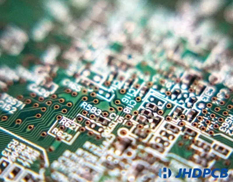
In the fast-evolving world of portable electronics, the tablet stands as a testament to innovation, blending functionality with sleek design. At the heart of every high-performance tablet lies a meticulously engineered Printed Circuit Board (PCB). For companies striving to launch the next generation of tablets, a robust, efficient, and reliable PCB solution is not just an advantage—it's a necessity. Zero One Solution Limited, a leader in PCB assembly solutions since 2011, is uniquely positioned to address these critical needs. From initial concept to mass production, our comprehensive Tablet PCB Solution empowers you to transform groundbreaking ideas into market-ready products with unparalleled speed and precision.
The Evolution and Importance of Tablet PCBs
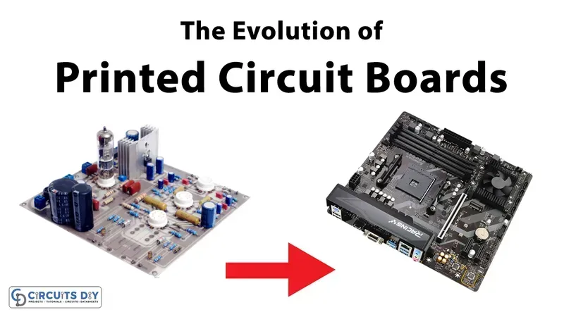
Tablet PCB Evolution
Tablet Printed Circuit Boards (PCBs) are the indispensable foundation of modern portable computing, embodying a remarkable evolution driven by an unrelenting pursuit of miniaturization, heightened performance, and superior power efficiency. These intricate, multi-layered circuit boards are far more than mere components; they are the central nervous system that orchestrates every function within a tablet, from processing power and connectivity to display management and battery life. Their ongoing development has been critical in transforming bulky, limited devices into the sleek, powerful, and ubiquitous tablets we rely on today, making them a pivotal factor in the continuous innovation and market success of tablet technology.
Era
Key PCB Evolution
Impact on Tablet Functionality
Early Tablets (2000s)
Larger form factors, fewer layers, focus on basic functionality.
Enabled initial portability, but limited performance and battery life due to larger components and less optimized layouts.
Miniaturization and Density The demand for thinner, lighter tablets has pushed PCB technology towards higher integration, utilizing HDI (High-Density Interconnect) and advanced stacking techniques to pack more components into significantly smaller footprints. This allows for sleeker designs without compromising functionality, a key differentiator in the competitive tablet market. According to a report by Statista, the global tablet market is projected to reach over 130 million units by 2027, underscoring the continuous need for advanced, space-efficient PCB solutions to support this growth.
Key Challenges in Tablet PCB Design and Manufacturing
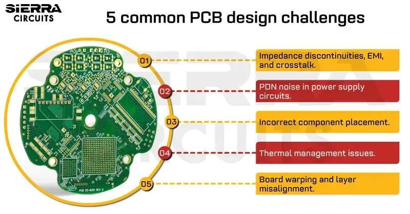
Challenges in Tablet PCB Design
Designing and manufacturing Printed Circuit Boards (PCBs) for tablets presents a unique set of engineering hurdles that demand specialized expertise and advanced technological solutions. Unlike larger electronic devices, tablets require ultra-compact, high-performance PCBs that can integrate complex functionalities within severely restricted physical envelopes, all while maintaining signal integrity and managing thermal dissipation effectively. These challenges are at the core of delivering the sleek form factors, extended battery life, and powerful processing capabilities that modern consumers expect from their mobile devices.
Miniaturization and Space Constraints Tablets are designed to be thin and lightweight, necessitating incredibly dense PCB layouts. This demands the use of High-Density Interconnect (HDI) technology, micro-vias, and fine-line circuitry to fit more components into a smaller area without compromising performance or reliability. Achieving this level of miniaturization while ensuring manufacturability is a significant engineering feat.
Thermal Management Despite their compact size, tablets house powerful processors and components that generate considerable heat. Effective thermal management on the PCB is crucial to prevent overheating, which can lead to performance degradation, reduced component lifespan, and even device failure. This involves strategic component placement, efficient heat dissipation pathways, and material selection with superior thermal conductivity.
Signal Integrity and Power Delivery With high operating frequencies and vast amounts of data transfer, maintaining signal integrity on tablet PCBs is paramount. Crosstalk, electromagnetic interference (EMI), and impedance mismatches can severely degrade performance. Simultaneously, ensuring stable and efficient power delivery to numerous components within a constrained space requires sophisticated power plane design and decoupling strategies to minimize noise and voltage drops.
High-Density Interconnection (HDI) Requirements HDI PCBs are indispensable for tablets due to their ability to accommodate higher component density and finer traces. This technology allows for more complex routing, smaller form factors, and improved electrical performance. However, manufacturing HDI boards requires precision equipment, stringent process control, and advanced material handling to achieve the necessary layer count and interconnection reliability.
Battery Integration and Power Efficiency Tablets rely heavily on long battery life, making power efficiency a critical PCB design consideration. The PCB must efficiently manage power distribution, minimize leakage currents, and support various low-power states without sacrificing performance. This often involves integrating sophisticated power management integrated circuits (PMICs) and optimizing circuit layouts for minimal power consumption.
Material Selection and Reliability Choosing the right PCB materials is vital for tablet longevity and performance. Materials must offer excellent dielectric properties for high-frequency signals, mechanical strength to withstand drops and bends, and thermal stability for consistent operation across varying temperatures. Ensuring the long-term reliability of these compact, high-stress boards is a continuous challenge.
Zero One Solution Limited's Comprehensive Tablet PCB Solution
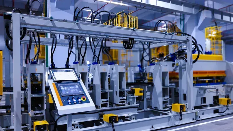
Tablet PCB Manufacturing Process
Zero One Solution Limited offers a truly comprehensive Tablet PCB Solution, seamlessly integrating every critical phase from initial design conceptualization through rapid prototyping to full-scale manufacturing and assembly. This end-to-end approach ensures that our clients receive a cohesive, optimized, and high-performance PCB tailored precisely to the intricate demands of modern tablet applications, thereby significantly de-risking the development process and accelerating market entry. Our expertise in miniaturization, power efficiency, and signal integrity allows us to deliver cutting-edge solutions that underpin the functionality and reliability of next-generation tablet devices.
Service Phase
Key Offerings
Client Benefit
PCB Design & Engineering
Schematic capture, layout optimization, DFM/DFA analysis, material selection
High-quality, defect-free assemblies, optimized production efficiency
Supply Chain Management
Global component sourcing, inventory optimization, logistics support
Cost-effective procurement, consistent material availability, reduced lead times
Our integrated workflow is designed to overcome the unique challenges of tablet PCB development, from ultra-compact footprints to demanding power management and high-speed data transmission requirements. By providing a single point of contact for all PCB-related needs, Zero One Solution Limited streamlines the entire process, allowing tablet innovators to focus on their core product vision while we handle the complexities of robust hardware enablement.
Integrated Design for Manufacturability (DFM) and Assembly (DFA) Our engineering team collaborates closely with clients from the design phase, integrating DFM and DFA principles to pre-emptively identify and resolve potential manufacturing challenges. This proactive approach ensures a seamless transition from design to production, minimizing revisions and optimizing manufacturing efficiency for tablet PCBs.
Advanced Material Expertise for Tablet PCB Reliability We leverage a deep understanding of advanced PCB materials, including high-Tg laminates, low-loss materials for high-frequency signals, and flexible substrates, to meet the specific performance and durability requirements of slim, portable tablet devices. This ensures superior signal integrity and thermal performance.
Scalable Production Capabilities for Diverse Tablet Volumes Whether it's a small batch of R&D prototypes or high-volume mass production, our facilities are equipped to scale production efficiently without compromising on quality or lead times. This flexibility supports various stages of a tablet's product lifecycle, from initial concept to market saturation.
Rapid Prototyping: Accelerating Your Tablet Development Cycle
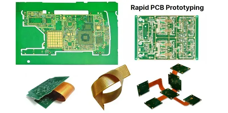
Rapid Prototyping Tablet PCB
In the dynamic tablet market, where innovation cycles are compressed and time-to-market is paramount, rapid prototyping of tablet PCBs is not merely an advantage but a critical necessity. It empowers engineers to swiftly validate designs, iterate on improvements, and mitigate costly errors early in the development phase, significantly accelerating the journey from concept to consumer-ready product. At Zero One Solution Limited, our specialized expertise in rapid-response R&D prototype manufacturing for tablet PCBs is engineered to drastically reduce your development timelines and gain a competitive edge.
Expedited Design Validation Our rapid prototyping capabilities allow for quick fabrication of initial tablet PCB designs. This enables engineers to perform immediate functional testing, identify potential flaws or optimizations, and validate design integrity against performance metrics with unprecedented speed.
Iterative Design Optimization The agility of our rapid prototyping process supports multiple design iterations in a fraction of the time compared to traditional methods. This iterative approach fosters continuous improvement, allowing for swift adjustments to component placement, trace routing, and overall board layout to enhance performance, thermal management, and power efficiency.
Reduced Development Costs By identifying and rectifying design issues in the prototyping phase, we significantly minimize the need for costly rework or redesigns during mass production. This proactive approach prevents expensive tooling changes and material waste, leading to substantial cost savings throughout the product development lifecycle.
Faster Time-to-Market Zero One Solution Limited's commitment to rapid prototyping directly translates to a faster time-to-market for your tablet innovations. By compressing the R&D cycle, we help you introduce your products to consumers sooner, capturing market share and responding swiftly to evolving consumer demands and technological trends.
Access to Advanced Technologies Our rapid prototyping services incorporate advanced manufacturing technologies, including High-Density Interconnect (HDI) and flexible PCB capabilities, crucial for the complex and miniaturized nature of modern tablet designs. This ensures that even early prototypes accurately reflect the characteristics of the final production board.
Advanced Manufacturing Capabilities for Tablet PCBA
Advanced HDI PCB for Tablets
Zero One Solution Limited’s advanced manufacturing capabilities are specifically engineered to meet the demanding requirements of high-performance tablet Printed Circuit Board Assembly (PCBA). Our state-of-the-art facilities and meticulous processes ensure the production of compact, powerful, and reliable tablet PCBs, critical for integrating complex functionalities within a confined form factor.
High-Density Interconnect (HDI) Technology HDI technology is fundamental to modern tablet PCBA, allowing for greater component density and miniaturization. Our capabilities include ultra-fine line and space, microvias, and buried/blind vias, enabling multi-layer boards that maximize functional integration while minimizing physical footprint. This is crucial for tablets where space is at a premium and high-speed signal integrity is paramount.
Flexible and Rigid-Flex PCB Solutions Tablets often require PCBs that can conform to non-planar enclosures or connect components across hinges and tight spaces. We specialize in both flexible and rigid-flex PCBs, offering unparalleled design freedom and robust mechanical performance. These solutions reduce connector count, improve reliability, and optimize space, contributing significantly to a tablet's sleek design and durability.
Precision Component Placement (SMT) Our advanced Surface Mount Technology (SMT) lines feature high-speed, high-precision pick-and-place machines capable of handling the smallest passive components and fine-pitch ICs with exceptional accuracy. This ensures precise component alignment and soldering, which is vital for the complex chipsets and intricate circuitry found in modern tablets, minimizing defects and enhancing overall performance.
Automated Optical Inspection (AOI) and X-ray Inspection Quality control is paramount. We employ automated optical inspection (AOI) for rapid and accurate detection of surface defects, solder joint issues, and component placement errors. Furthermore, X-ray inspection is utilized for internal layer alignment verification and solder joint integrity under Ball Grid Array (BGA) and other hidden components, guaranteeing the highest reliability for critical tablet functions.
Strict Quality Control and Testing Protocols Our comprehensive quality management system adheres to international standards (e.g., ISO 9001, IPC Class 2/3). Every tablet PCBA undergoes rigorous testing, including in-circuit testing (ICT), functional testing (FCT), and environmental stress testing (EST), to ensure compliance with performance specifications, thermal stability, and long-term reliability in diverse operating conditions. Our commitment to stringent quality control minimizes field failures and ensures superior product lifespan.
Global Supply Chain and Strategic Locations for Tablet PCB Solutions
Global Supply Chain Logistics
Zero One Solution Limited's strategic global presence, anchored by our Shenzhen headquarters and Dubai branch, is a cornerstone of our ability to deliver superior Tablet PCB Solutions. This dual-hub model ensures not only unparalleled access to the world's most robust electronics manufacturing ecosystem but also provides critical logistical advantages, minimizing lead times and optimizing resource allocation for our global clientele. This integrated approach ensures that from rapid prototyping to high-volume production, your tablet PCB projects benefit from a truly interconnected and efficient supply chain.
Location
Strategic Advantage
Impact on Tablet PCB Projects
Shenzhen, China (Headquarters)
Proximity to the heart of global electronics manufacturing; access to a vast network of component suppliers, advanced technology, and skilled labor.
Accelerated component sourcing, state-of-the-art manufacturing capabilities for HDI and flexible PCBs, reduced production costs, and rapid scalability for tablet PCB assembly.
Dubai, UAE (Branch Office)
Strategic gateway between East and West; efficient logistics hub for global distribution; access to emerging markets.
Streamlined global distribution, enhanced customer support for EMEA and surrounding regions, diversified supply chain resilience, and faster delivery times for finished tablet PCBA products worldwide.
This geographical synergy empowers Zero One Solution Limited to offer a resilient and adaptable supply chain for tablet PCB solutions, capable of navigating geopolitical shifts and ensuring consistent, high-quality output regardless of project scale or complexity. Our global footprint is designed to translate into tangible benefits for our clients: reduced time-to-market, enhanced cost-efficiency, and unwavering reliability in delivering advanced tablet PCB solutions.
Why Choose Zero One Solution Limited for Your Tablet PCB Needs?
Choosing the right partner for your tablet PCB needs is paramount to the success of your product. Zero One Solution Limited stands out as a premier provider, offering an unparalleled blend of experience, advanced capabilities, and a client-centric approach that ensures your tablet innovations move from concept to market efficiently and reliably. Our dedication to rapid prototyping, stringent quality, and global accessibility positions us as the ideal partner to navigate the complexities of modern tablet electronics.
Unrivaled Expertise in Tablet PCBA With over a decade of specialized experience since 2011, Zero One Solution Limited has been at the forefront of PCB assembly solutions, particularly for compact and high-performance devices like tablets. Our engineers possess deep knowledge in miniaturization, HDI technology, and efficient power management, critical for leading-edge tablet designs. We understand the nuances of integrating complex components into confined spaces while maintaining signal integrity and thermal efficiency.
Accelerated Time-to-Market with Rapid Prototyping Our core strength lies in rapid-response R&D prototype manufacturing. We drastically reduce your product development cycles, allowing for quicker iterations and faster validation of your tablet designs. This agility is crucial in the fast-paced consumer electronics market, giving you a significant competitive edge by bringing your innovations to market sooner.
State-of-the-Art Manufacturing and Quality Assurance We operate with cutting-edge facilities capable of handling the most advanced tablet PCB requirements, including multi-layer PCBs, flexible circuits, and fine-pitch components. Our commitment to quality is unwavering, with rigorous testing protocols and adherence to international standards (e.g., ISO 9001, IPC Class 2/3) ensuring every PCBA we produce meets the highest levels of reliability and performance.
Feature
Zero One Solution Limited Advantage
Client Benefit
Rapid Prototyping
5-7 day turnaround for prototypes
Reduced development costs, faster product validation
HDI/Multi-layer PCBA
Supports up to 30+ layers, advanced routing
Enables compact, high-performance tablet designs
Global Supply Chain
Shenzhen HQ & Dubai branch
Optimized logistics, diverse material sourcing, cost-effectiveness
Experienced engineering and project management teams
Seamless communication, expert guidance throughout the project
Frequently Asked Questions About Tablet PCB Solutions
Navigating the complexities of Tablet PCB solutions often raises pertinent questions for developers and manufacturers. This section addresses the most common inquiries regarding tablet PCB design, manufacturing processes, lead times, and quality assurance, providing clear and concise answers to empower informed decision-making for your next tablet project.
What are the primary design considerations for high-performance Tablet PCBs? The primary design considerations for high-performance Tablet PCBs revolve around miniaturization, thermal management, signal integrity, and power efficiency. This includes employing High-Density Interconnect (HDI) technology for compact layouts, strategic component placement for heat dissipation, impedance control for high-speed signals, and efficient power plane design to maximize battery life and performance in a constrained space.
How does Zero One Solution Limited ensure quality assurance for Tablet PCB manufacturing? Zero One Solution Limited ensures rigorous quality assurance for Tablet PCB manufacturing through a multi-stage process. This includes stringent Incoming Quality Control (IQC) for raw materials, in-process inspections (IPC Class 2/3 standards), Automated Optical Inspection (AOI), X-ray inspection for BGA and CSP components, Electrical Test (ET), and final functional testing (FCT) tailored to client specifications. Our ISO 9001 certified facilities and experienced engineering teams uphold the highest standards.
What is the typical lead time for Tablet PCB prototyping and mass production? Lead times for Tablet PCB solutions vary depending on complexity and order volume. For rapid prototyping, Zero One Solution Limited typically delivers within 3-7 business days for standard designs, leveraging our agile R&D capabilities. Mass production lead times generally range from 2-4 weeks, depending on component availability, board layers, and specific manufacturing requirements. We work closely with clients to meet their critical timelines.
Can Zero One Solution Limited accommodate flexible and rigid-flex PCB designs for tablets? Yes, Zero One Solution Limited specializes in accommodating both flexible and rigid-flex PCB designs, which are increasingly crucial for modern tablets due to their compact form factors and complex interconnections. Our advanced manufacturing capabilities support various stack-ups and materials, enabling innovative product designs that require dynamic bending or space-saving solutions for compact tablet architectures.
What post-assembly services does Zero One Solution Limited provide for Tablet PCBA? Beyond manufacturing, Zero One Solution Limited offers comprehensive post-assembly services for Tablet PCBA to ensure readiness for market. This includes conformal coating for environmental protection, functional testing (FCT) to validate performance, final assembly into enclosures, packaging, and global logistics support from our strategic locations in Shenzhen and Dubai, providing a true one-stop solution for tablet manufacturers.
In conclusion, the success of modern tablet devices hinges on the quality and efficiency of their underlying PCB solutions. Zero One Solution Limited's comprehensive Tablet PCB Solution offers a distinct competitive advantage, combining our deep expertise in rapid prototyping, precision manufacturing, and global supply chain management. We are committed to being your strategic partner, enabling you to bring innovative tablet products to market faster and more reliably. Don't let PCB complexities slow down your innovation. Contact Zero One Solution Limited today to discuss how our tailored Tablet PCB Solution can accelerate your next project. Visit our website or reach out to our team for a consultation – let's build the future of tablets, together.