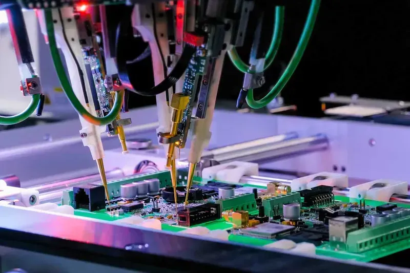
In the fast-evolving world of mobile technology, the smartphone motherboard stands as the intricate brain, dictating performance, connectivity, and overall user experience. For innovators and device manufacturers, the journey from concept to a functional smartphone hinges critically on a robust, efficient, and reliable motherboard solution. At Zero One Solution Limited, we understand this paramount importance. As a leading PCB solution provider founded in 2011, headquartered in Shenzhen with a strategic branch in Dubai, we specialize in rapid-response R&D prototype manufacturing. This article delves into the complexities of smartphone motherboard solutions, showcasing how our unparalleled expertise and one-stop services, from PCB design to manufacturing and assembly, empower our clients to bring revolutionary mobile devices to market with unprecedented speed and efficiency.
The Core of Modern Smartphones: Understanding the Motherboard
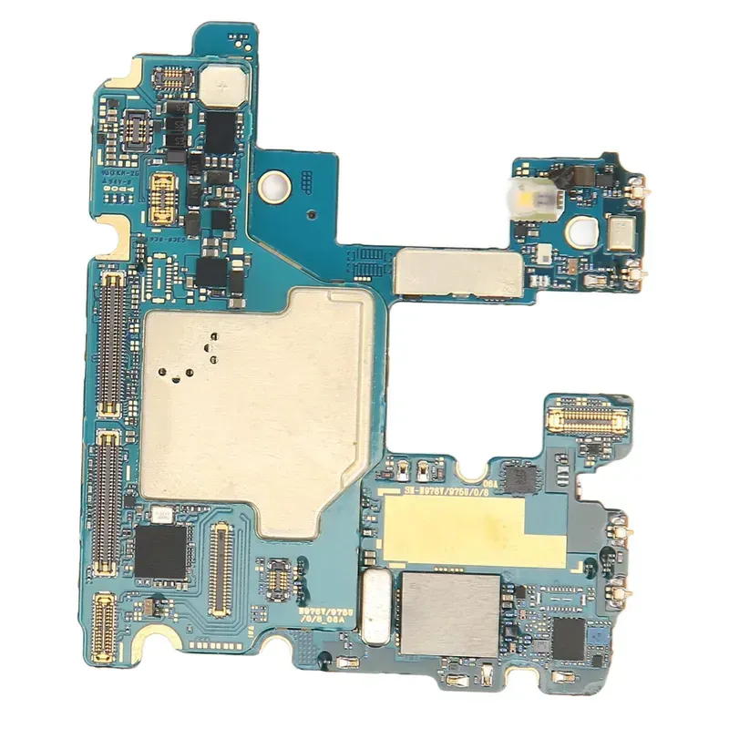
Smartphone Motherboard
The smartphone motherboard, often referred to as the main logic board or PCB, is the quintessential nerve center of any modern mobile device. Far from a simple circuit board, it's a densely packed marvel of engineering that orchestrates every function, from processing complex data and managing power distribution to facilitating connectivity and supporting user interface interactions. Its intricate design, driven by relentless demands for miniaturization, high integration, and peak performance, directly dictates a smartphone's capabilities, reliability, and ultimately, its market success. For device manufacturers, understanding and expertly navigating the complexities of this core component is paramount.
Miniaturization Imperative Modern smartphones demand extreme component density, requiring multi-layered PCBs with micro-vias and fine-pitch components to fit powerful functionalities into incredibly thin form factors. This dictates highly specialized design and manufacturing processes.
Integration Density A single smartphone motherboard integrates a vast array of critical components, including the System-on-Chip (SoC), memory modules (RAM and storage), power management ICs (PMICs), wireless communication modules (Wi-Fi, Bluetooth, 5G), camera modules, and various sensors. Seamless integration without signal interference or thermal issues is a monumental challenge.
Performance Demands Users expect instantaneous response times, fluid multitasking, and high-fidelity media consumption. The motherboard must support high-speed data transfer, efficient power delivery to hungry components, and effective heat dissipation to maintain optimal performance under heavy loads.
Power Efficiency Battery life is a primary concern for smartphone users. The motherboard design must incorporate advanced power management strategies to minimize consumption across all integrated circuits, extending device uptime without compromising performance.
In essence, the smartphone motherboard is a testament to cutting-edge electronic engineering. Its development requires a deep understanding of advanced materials, precise manufacturing techniques, and rigorous testing protocols to ensure every component functions harmoniously within a confined space, delivering the seamless experience consumers expect. This complexity underscores why expert PCB solution providers are indispensable in the competitive smartphone market.
Challenges in Smartphone Motherboard Design and Manufacturing
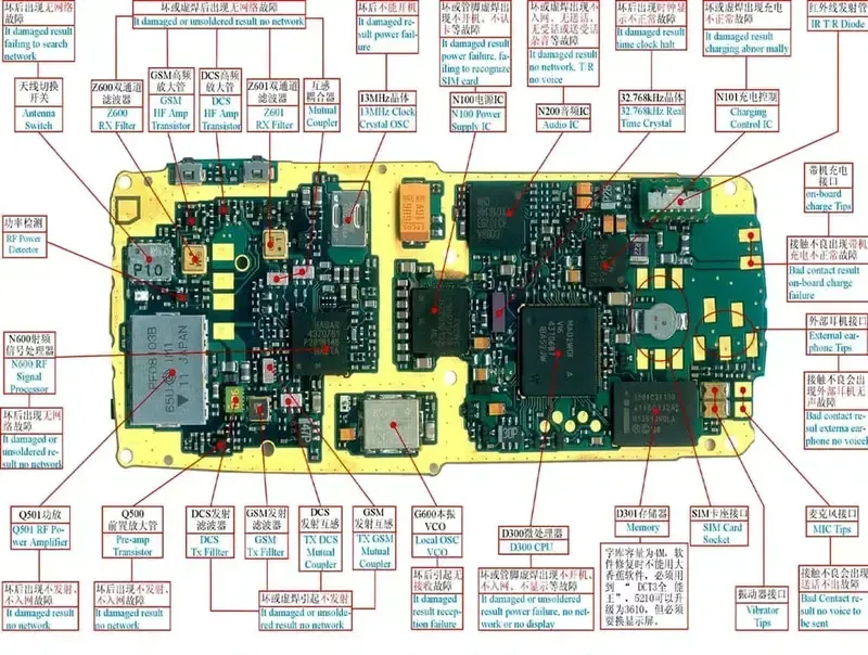
Mobile Device PCBA
Designing and manufacturing smartphone motherboards presents a myriad of intricate challenges, demanding specialized expertise to overcome. The relentless pursuit of miniaturization, coupled with escalating performance requirements, pushes the boundaries of engineering, making these compact circuits one of the most complex components in consumer electronics. Successfully navigating these hurdles requires a deep understanding of advanced PCB design principles, material science, and manufacturing precision.
Space Constraints and Miniaturization Smartphones are defined by their compact form factors, which necessitate an extreme level of component density on the motherboard. This demands multi-layer PCBs, micro-vias, and fine-pitch components, pushing manufacturing tolerances to their limits. The challenge lies in integrating increasing functionality into diminishing space without compromising performance or reliability. For instance, modern smartphone motherboards often feature 10-14 layers with trace widths as fine as 25-50 microns, far exceeding typical industrial PCB requirements.
Thermal Management Packing powerful processors, modems, and memory into a small enclosure generates significant heat. Effective thermal management is critical to prevent performance throttling, extend component lifespan, and ensure user safety. This involves innovative heat dissipation strategies, such as integrated heat pipes, graphite sheets, and advanced thermal interface materials, designed to channel heat away from critical components while maintaining a thin profile. Inadequate thermal design can lead to rapid performance degradation and system instability.
Signal Integrity and Power Efficiency High-speed data transfer within the motherboard (e.g., between the SoC, RAM, and storage) is susceptible to signal degradation, crosstalk, and electromagnetic interference (EMI). Maintaining signal integrity requires precise impedance control, optimized trace routing, and proper grounding. Simultaneously, maximizing battery life demands exceptional power efficiency, which involves meticulous power delivery network (PDN) design, efficient voltage regulators, and dynamic power management techniques to minimize energy consumption across all integrated circuits. This dual challenge is particularly acute in 5G-enabled devices, where higher frequencies amplify signal integrity concerns and power demands.
Integration of Complex Components A smartphone motherboard is a highly integrated system, incorporating a System-on-Chip (SoC), various memory modules (RAM, ROM), power management ICs (PMICs), RF transceivers, Wi-Fi/Bluetooth modules, and an array of sensors (accelerometer, gyroscope, camera modules). The seamless integration of these disparate components, often from multiple vendors, requires extensive validation and compatibility testing. The failure of even a single component to interact correctly can compromise the entire device's functionality.
Manufacturing Precision and Yield Producing these highly complex motherboards at scale with high yield rates is a significant manufacturing challenge. The intricate designs, minute features, and high component density demand state-of-the-art manufacturing facilities, advanced assembly techniques like fine-pitch SMT (Surface Mount Technology), and rigorous automated optical inspection (AOI) to detect defects. Maintaining consistent quality across millions of units while controlling costs requires sophisticated process control and continuous improvement methodologies.
Zero One Solution Limited's Comprehensive Smartphone Motherboard Solution
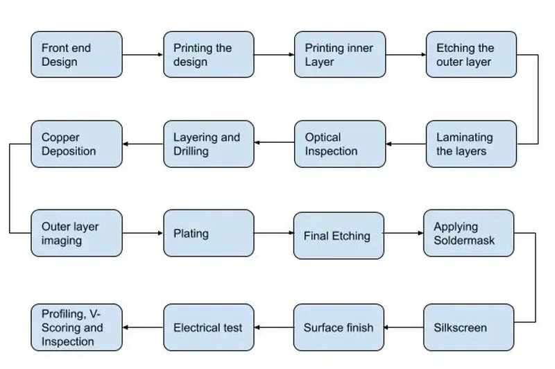
PCB Design and Manufacturing
Zero One Solution Limited provides an unparalleled, comprehensive smartphone motherboard solution, meticulously designed to navigate the intricate challenges of mobile device engineering. As a veteran PCB solution provider, our 'one-stop service' model integrates every critical stage, from initial concept to high-volume production, ensuring seamless project execution and superior outcomes for even the most complex custom smartphone circuits. We empower innovators to accelerate product development and bring cutting-edge mobile solutions to market with efficiency and reliability.
Integrated PCB Design and Layout Optimization Our expertise begins at the fundamental design phase. We specialize in compact, multi-layer PCB designs, meticulously optimizing layouts for signal integrity, power distribution, and thermal management within the stringent space constraints of smartphones. Our engineers leverage advanced DFM (Design for Manufacturability) and DFL (Design for Layout) principles to prevent common manufacturing pitfalls and enhance overall board performance and reliability.
Strategic Component Sourcing and Management Leveraging our extensive global supply chain network, Zero One Solution Limited ensures access to high-quality, authentic components at competitive prices. We manage the entire sourcing process, from BOM optimization and vendor qualification to inventory management, mitigating supply chain risks and ensuring the availability of specialized ICs, connectors, and passive components essential for advanced mobile device PCBA.
Rapid Prototyping for Accelerated Development Speed to market is paramount in the mobile industry. Our rapid prototyping capabilities allow for swift iteration and validation of smartphone motherboard designs. Within days, clients can receive functional prototypes, enabling crucial testing and design refinement, significantly reducing development cycles, and providing a critical competitive advantage.
Advanced Manufacturing and Assembly (PCBA) Our state-of-the-art manufacturing facilities in Shenzhen are equipped with cutting-edge SMT lines and advanced assembly technologies tailored for high-density, miniature PCBA. We handle complex soldering challenges, fine-pitch components, and multi-board integration, ensuring precision and consistency in every smartphone motherboard produced, from small batch runs to high-volume production.
Rigorous Quality Assurance and Testing Quality and reliability are non-negotiable. Our comprehensive quality assurance protocols include in-circuit testing (ICT), functional testing (FCT), X-ray inspection, and environmental stress testing. Every smartphone motherboard undergoes stringent validation to meet industry standards and specific client requirements, guaranteeing robust performance and longevity in the demanding mobile environment.
Service Aspect
Zero One Solution Limited's Approach
Client Benefit
PCB Design
Compact, multi-layer optimization with DFM/DFL
Maximized performance, reduced errors
Component Sourcing
Global network, authenticated parts, cost-efficient
Supply chain reliability, competitive pricing
Prototyping
Rapid iteration, functional models in days
Faster time-to-market, agile development
Manufacturing
High-density SMT, advanced assembly
Precision, scalability, consistent quality
Quality Control
Comprehensive testing (ICT, FCT, X-ray)
Guaranteed reliability, long-term performance
Rapid Prototyping: Accelerating Your Smartphone Product Development
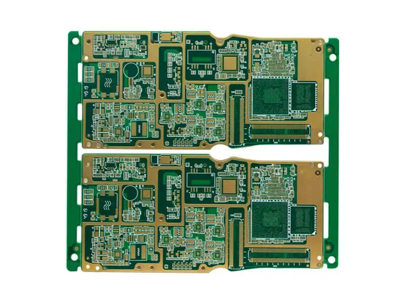
Smartphone Motherboard Prototype
In the hyper-competitive smartphone market, time-to-market is a critical differentiator. Zero One Solution Limited's rapid prototyping capabilities are engineered to dramatically accelerate your smartphone product development cycle, transforming conceptual designs into tangible, testable prototypes with unprecedented speed. This agile approach is fundamental to validating complex motherboard designs, iterating quickly based on performance insights, and gaining a crucial competitive edge in bringing innovative mobile devices to consumers faster.
Prototyping Stage
Traditional Approach
Zero One Solution's Rapid Prototyping
Design Validation
Slow, sequential iterations; often requires multiple complete fabrication cycles.
Manual assembly and debugging; prone to delays and errors.
Automated precision assembly (SMT); specialized tools for efficient component integration and verification.
Performance Testing
Delayed until full prototype completion; limited opportunities for early optimization.
Early-stage testing of sub-assemblies and functional blocks; pre-emptive issue identification and resolution.
Cost Efficiency
Higher costs due to re-spins and extended development cycles.
Reduced costs through minimized re-spins and optimized resource utilization.
Time-to-Market Impact
Significantly prolonged development timelines, missing market windows.
Accelerated time-to-market, enabling first-mover advantage and market capture.
Our commitment to agile development as a core strength of our PCB solution provider services means leveraging advanced technologies and streamlined processes. This includes high-speed PCB fabrication, advanced SMT (Surface Mount Technology) assembly for densely packed smartphone motherboards, and rigorous in-process quality checks. By integrating DFM (Design for Manufacturability) and DFL (Design for Layout) principles from the outset, we ensure that prototypes are not just functional but are also optimized for eventual high-volume production, mitigating risks and costs down the line.
// Example: Simplified Rapid Prototyping Workflow for Smartphone Motherboard
function accelerateProductDevelopment(design_specifications) {
    let pcb_layout = designOptimization(design_specifications);
    let prototype_boards = rapidFabrication(pcb_layout, "high-speed_materials");
    let assembled_pcbas = automatedSMTAssembly(prototype_boards, "miniature_components");
    let validation_results = functionalTesting(assembled_pcbas);

    if (validation_results.pass) {
        console.log("Prototype validated. Ready for scaled production.");
        return "Success";
    } else {
        console.log("Issues found. Initiating rapid iteration on design.");
        return accelerateProductDevelopment(refineDesign(design_specifications, validation_results));
    }
}
Quality Assurance and Reliability in Mobile Device PCBA
Mobile Device PCBA Testing
Ensuring the robustness and longevity of smartphone motherboards is paramount in the fiercely competitive mobile device market. At Zero One Solution Limited, our commitment to unyielding quality assurance and reliability for Mobile Device PCBA components underpins every smartphone motherboard solution we deliver. This dedication goes beyond mere compliance; it's an ingrained philosophy that drives our comprehensive testing protocols and adherence to the most stringent industry standards, guaranteeing that every device built on our PCBA platform performs optimally and endures the rigors of daily use.
What are the critical aspects of Design for Manufacturability (DFM) for smartphone motherboards? DFM for smartphone motherboards focuses on optimizing the design to facilitate efficient, cost-effective, and high-yield manufacturing. Key aspects include optimizing component placement for automated assembly, ensuring adequate spacing for soldering and inspection, standardizing part selection to leverage economies of scale, and designing for efficient thermal dissipation. It also involves considerations for panelization, fiducials, and test points to streamline the production process and reduce potential manufacturing defects, ultimately enhancing the reliability of the mobile device PCBA.
How does Design for Layout (DFL) contribute to the reliability of smartphone motherboards? DFL is crucial for the electrical integrity and reliability of smartphone motherboards. It involves meticulous routing of traces to minimize signal integrity issues like crosstalk and impedance mismatches, strategic placement of power and ground planes to reduce noise, and careful consideration of component proximity to mitigate electromagnetic interference (EMI). Effective DFL ensures stable power delivery, high-speed data transmission, and overall system stability, directly impacting the performance and longevity of the mobile device PCBA by preventing common electrical failures.
What advanced testing methodologies are employed to ensure smartphone motherboard quality? Advanced testing methodologies for smartphone motherboard solutions include Automated Optical Inspection (AOI) for visual defect detection, Automated X-ray Inspection (AXI) for hidden solder joint analysis (especially for BGA components), In-Circuit Testing (ICT) to verify component presence and electrical connectivity, and Functional Testing (FCT) to simulate real-world operational scenarios. Environmental Stress Screening (ESS) like thermal cycling and vibration testing are also employed to identify potential weaknesses under extreme conditions, ensuring the mobile device PCBA's resilience and long-term reliability.
What industry standards are critical for smartphone motherboard reliability? Adherence to industry standards is non-negotiable for smartphone motherboard reliability. Key standards include IPC-A-610 (Acceptability of Electronic Assemblies) for workmanship criteria, IPC-2221 (Generic Standard on PCB Design) for design guidelines, and JEDEC standards for component reliability testing and qualification. Compliance with relevant electromagnetic compatibility (EMC) and radio frequency (RF) regulations (e.g., FCC, CE) is also vital to ensure the device operates without interference and meets global regulatory requirements, thereby guaranteeing a robust smartphone motherboard solution.
How does Zero One Solution Limited ensure long-term reliability for its smartphone motherboard solutions? Zero One Solution Limited ensures long-term reliability through a holistic approach encompassing stringent material selection, validated component sourcing, meticulous DFM and DFL processes, and comprehensive multi-stage testing protocols. We integrate reliability modeling and accelerated life testing into our development cycles, proactively identifying and mitigating potential failure points. Our strategic global supply chain and continuous improvement initiatives, based on field data and customer feedback, further reinforce the durability and longevity of our mobile device PCBA solutions, providing peace of mind for our clients.
The Global Advantage: Zero One Solution Limited's Strategic Presence
Zero One Solution Limited's strategic global presence is a cornerstone of our ability to deliver superior smartphone motherboard solutions. Our headquarters in Shenzhen, China, the undisputed epicenter of electronic manufacturing, combined with a crucial branch office in Dubai, enables us to harness a sophisticated global supply chain network. This dual strategic positioning ensures unparalleled access to cutting-edge resources, high-quality materials, and diverse support, allowing us to provide clients worldwide with exceptionally efficient and cost-effective mobile device PCBA solutions, solidifying our reputation as a truly global PCB solution provider.
Strategic Location
Key Advantage
Impact on Smartphone Motherboard Solutions
Shenzhen, China (Headquarters)
Global Manufacturing Hub, Innovation Ecosystem, Skilled Labor Pool
Access to advanced manufacturing technologies, rapid material sourcing, competitive pricing, and a vast talent pool for complex PCB assembly.
Optimized Global Supply Chain Our presence in Shenzhen grants immediate access to a robust ecosystem of component suppliers, raw material providers, and advanced manufacturing facilities. This significantly reduces lead times and logistics costs, critical for high-volume production of smartphone motherboards. Furthermore, it ensures flexibility and resilience against supply chain disruptions, a common challenge in the electronics industry.
Strategic Bridging Point The Dubai branch office serves as a vital bridge for our global operations, particularly for clients in the Middle East, Africa, and Europe. This facilitates localized support, streamlines communication, and accelerates distribution, ensuring that our innovative smartphone motherboard solutions reach our international clientele efficiently and reliably.
Cost-Effectiveness and Scalability Leveraging the manufacturing efficiencies of Shenzhen allows us to offer highly competitive pricing without compromising quality. This, combined with our global reach, means we can scale production from rapid prototypes to mass manufacturing for smartphone motherboards, meeting diverse client demands while optimizing their investment.
FAQs about Smartphone Motherboard Solutions
What are the primary considerations for smartphone motherboard design to ensure optimal performance? Optimal smartphone motherboard design requires a delicate balance of miniaturization, power efficiency, thermal management, and high-speed signal integrity. Key considerations include component placement for minimal trace lengths and reduced electromagnetic interference (EMI), intelligent power delivery networks (PDN) to prevent voltage drops, and effective thermal dissipation strategies. Furthermore, selecting the right materials for the PCB substrate and optimizing layer stack-up are crucial for signal integrity at high frequencies, directly impacting overall device performance and reliability.
How does rapid prototyping benefit the development of smartphone motherboards? Rapid prototyping is indispensable for smartphone motherboard development, significantly accelerating the design-to-market cycle. It allows engineers to quickly iterate on designs, test functionality, validate performance, and identify potential issues early in the development phase. This iterative approach minimizes costly rework later, reduces time-to-market, and enables faster adaptation to evolving technological demands, ensuring a competitive edge in the fast-paced mobile industry. It provides a tangible prototype for physical and electrical evaluation before mass production.
What specific quality control measures are applied to smartphone motherboard manufacturing? Stringent quality control measures are applied throughout the smartphone motherboard manufacturing process to ensure reliability and longevity. These include Design for Manufacturability (DFM) and Design for Layout (DFL) analyses at the pre-production stage to identify and mitigate potential manufacturing issues. During production, advanced testing methodologies such as Automated Optical Inspection (AOI), X-ray inspection for hidden solder joints, In-Circuit Testing (ICT), and Functional Testing (FCT) are employed. Furthermore, thermal cycling, vibration testing, and drop tests simulate real-world conditions to guarantee robustness and adherence to industry standards like IPC Class 2/3.
Why is a global supply chain advantageous for smartphone motherboard solutions? A global supply chain provides significant advantages for smartphone motherboard solutions by ensuring access to a wider range of high-quality components, specialized manufacturing capabilities, and competitive pricing. Strategic locations like Shenzhen (China) and Dubai, as leveraged by Zero One Solution Limited, facilitate efficient logistics, reduced lead times, and the ability to source specialized materials or components globally. This global reach minimizes risks associated with single-source reliance, enhances flexibility in production, and ultimately offers more cost-effective and innovative solutions to clients worldwide, regardless of their operational base.
What are the common challenges in manufacturing mobile device PCBA and how are they overcome? Manufacturing mobile device PCBA presents several challenges, primarily due to extreme miniaturization, high component density, fine-pitch components (e.g., BGA, QFN), and the need for robust thermal management. These are overcome through precision manufacturing techniques such as advanced SMT (Surface Mount Technology) processes with high-accuracy pick-and-place machines, sophisticated reflow soldering profiles, and meticulous inspection protocols. Expertise in managing signal integrity in multi-layer PCBs and implementing efficient cooling solutions (e.g., heat pipes, graphite sheets) is also crucial. Utilizing a 'one-stop service' provider with specialized experience in complex PCBA, like Zero One Solution Limited, is essential to navigate these challenges effectively.
The smartphone motherboard is more than just a component; it's the heartbeat of modern mobile innovation. At Zero One Solution Limited, we pride ourselves on being the trusted partner who can translate your most ambitious designs into tangible, high-performance realities. Our commitment to rapid prototyping, stringent quality control, and comprehensive one-stop services, from PCB design to manufacturing and assembly, positions us uniquely to support the dynamic needs of the mobile device industry. Empower your next-generation smartphone with a foundation built on precision, reliability, and speed. Contact Zero One Solution Limited today to discuss your smartphone motherboard solution needs and let us accelerate your product's journey from concept to market leader.