Optical Communication Monitoring System PCB Solution
2025.08.12
In the rapidly evolving landscape of modern telecommunications, optical communication systems form the backbone of global data transfer. Ensuring their uninterrupted and optimal performance is paramount, which is where sophisticated monitoring systems come into play. At the heart of these critical monitoring infrastructures are highly specialized Printed Circuit Boards (PCBs). Zero One Solution Limited, a leader in rapid prototyping and comprehensive PCB solutions since 2011, understands the unique demands of this sector. This article delves into how our expertise in PCB design, manufacturing, and assembly provides a robust foundation for next-generation optical communication monitoring systems, ensuring reliability, speed, and precision.
The Critical Role of PCBs in Optical Communication Monitoring
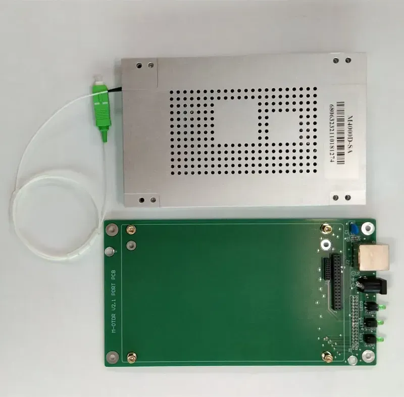
Optical Communication Monitoring System PCB
In the intricate world of optical communication, where data transmission speed and accuracy are paramount, Printed Circuit Boards (PCBs) are not just components but the foundational backbone enabling the precise signal processing and data acquisition critical for reliable monitoring systems. High-performance PCBs are essential for maintaining signal integrity, minimizing noise, and ensuring the stable operation of sensitive optical modules, directly impacting the system's ability to detect, analyze, and manage the vast flows of optical data with unparalleled precision.
Signal Integrity and High-Frequency Performance Optical communication operates at extremely high frequencies, demanding PCBs that can maintain signal integrity across long traces. Specialized PCB materials with low dielectric loss and controlled impedance are crucial to prevent signal degradation, reflections, and crosstalk, which can severely impact data accuracy and system reliability. Our designs rigorously account for these parameters, ensuring pristine signal transmission from optical transducer to digital processing unit.
PCB Feature
Impact on Optical Communication Monitoring
Benefit
Controlled Impedance Traces
Minimizes signal reflections and distortion at high frequencies.
Ensures accurate data transmission and reception, vital for monitoring system precision and reliability (e.g., BER testing).
Low Dielectric Loss Materials (e.g., Rogers, Isola)
Reduces signal attenuation over long distances and at high speeds.
Preserves signal strength and clarity, allowing for more sensitive and accurate monitoring of optical network performance (e.g., OSNR monitoring).
Multi-Layer Design
Provides effective shielding and isolation for sensitive analog and digital signals.
Mitigates electromagnetic interference (EMI) and crosstalk, enhancing signal-to-noise ratio (SNR) for superior monitoring accuracy and fewer false positives.
Furthermore, the integration of analog-to-digital converters (ADCs), digital signal processors (DSPs), and high-speed memory on a single board necessitates meticulous layout and routing. PCBs in optical communication monitoring systems must also effectively manage thermal dissipation from high-power components, preventing performance degradation and ensuring long-term operational stability in demanding environments. This comprehensive approach to PCB design and manufacturing is what distinguishes Zero One Solution Limited, delivering robust, high-performance solutions tailored for the exacting requirements of optical networks.
Key Challenges in Optical Communication Monitoring PCB Design
PCB Design Engineer at Work
Designing Printed Circuit Boards (PCBs) for optical communication monitoring systems presents a formidable array of engineering challenges, primarily due to the intricate interplay of high-speed data transmission, sensitive analog signals, and the need for unwavering reliability. The very essence of these systems demands precision at every stage, from material selection to layout, as any deviation can compromise signal integrity and the accuracy of critical monitoring data. Overcoming these hurdles is paramount for ensuring the stable and efficient operation of global optical networks, which form the backbone of modern digital infrastructure.
Signal Integrity at High Frequencies Optical communication systems operate at gigabit per second speeds, making signal integrity a critical concern. PCB traces must be designed with precise impedance control to prevent reflections, crosstalk, and signal degradation. This involves careful consideration of trace width, spacing, and dielectric materials, often necessitating advanced routing techniques and multilayer boards to minimize signal loss and maintain data fidelity across complex circuits. The challenge is amplified by the need to transmit both high-speed digital and sensitive analog signals on the same board without interference, requiring meticulous isolation and shielding strategies.
Effective Noise Reduction Strategies Optical communication monitoring systems are highly susceptible to noise, which can obscure subtle signal changes and lead to inaccurate readings. Sources of noise include power supply fluctuations, electromagnetic interference (EMI) from adjacent components, and even thermal noise. Effective noise reduction involves a multi-pronged approach, including optimized grounding schemes, strategic component placement to minimize coupling, the use of low-noise components, and robust power delivery networks (PDNs) that ensure stable voltage rails. Advanced filtering techniques are also crucial for isolating desired signals from unwanted noise.
Comprehensive Thermal Management The high component density and power dissipation in optical communication monitoring PCBs can lead to significant heat generation. Unmanaged heat can degrade component performance, shorten lifespan, and introduce measurement errors. Effective thermal management involves selecting materials with good thermal conductivity, incorporating heat sinks, employing thermal vias for efficient heat dissipation, and optimizing PCB layout to facilitate airflow. Simulation tools are often used to predict thermal hotspots and ensure that the design can safely dissipate the generated heat under various operating conditions, maintaining system stability and reliability.
Zero One Solution Limited's Expertise in High-Speed PCB Solutions
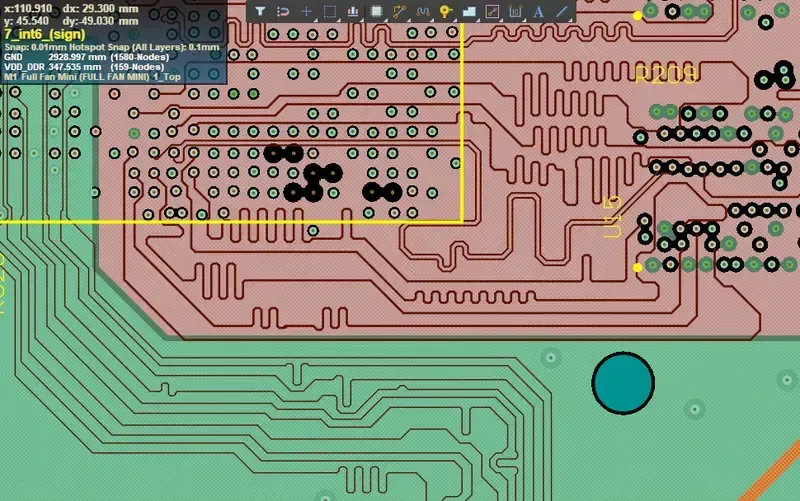
High-Speed PCB Board
Zero One Solution Limited stands at the forefront of high-speed PCB solutions, delivering unparalleled expertise critical for the demanding requirements of optical communication monitoring systems. Our deep understanding of signal integrity, power integrity, and thermal management, combined with advanced manufacturing capabilities, enables us to produce PCBs that reliably support ultra-fast data rates and precision sensing, which are essential for the next generation of optical networks.
Aspect
Zero One Solution's Advantage
Benefit for Optical Communication Monitoring
High-Speed Material Selection
Access to a wide range of low-loss dielectric materials (e.g., Rogers, Panasonic Megtron)
Minimizes signal attenuation and distortion, ensuring accurate high-frequency data transmission.
Advanced Stack-up Design
Multi-layer stack-up optimization with controlled impedance and isolation techniques
Enhances signal integrity, reduces crosstalk, and improves electromagnetic compatibility (EMC) in complex systems.
Precision Fabrication
Sub-micron trace and space capabilities, highly accurate drilling and plating processes
Integrated thermal vias, copper pours, and heat sinks; expertise in materials with high thermal conductivity
Dissipates heat effectively from high-power components, preventing performance degradation and extending system lifespan.
Signal Integrity Analysis (SIA)
Advanced simulation tools for pre-layout and post-layout analysis (e.g., Ansys HFSS, Cadence Sigrity)
Identifies and mitigates potential signal integrity issues early in the design cycle, saving time and cost.
Why is Zero One Solution Limited uniquely positioned for high-speed optical communication PCBs? Our unique position stems from a decade of specialized experience in rapid-response R&D prototyping, coupled with a strategic presence in Shenzhen and Dubai, granting us unparalleled access to advanced materials and a global supply chain. We combine rigorous design methodologies with cutting-edge manufacturing processes, specifically tailored to address the stringent signal integrity and thermal demands of optical communication systems.
What specific technologies do you employ for high-speed signal integrity? We leverage advanced design tools for comprehensive Signal Integrity (SI) and Power Integrity (PI) analysis, including pre-layout and post-layout simulations. Our technology suite includes controlled impedance routing, differential pair matching, precise layer stack-up optimization, and careful material selection to minimize loss and dispersion at high frequencies, ensuring signal fidelity across the board.
How do you ensure thermal reliability in compact optical monitoring systems? Thermal reliability is achieved through a multi-faceted approach. We integrate thermal vias, employ specialized thermal management materials with high thermal conductivity, and optimize copper pour designs to dissipate heat efficiently. Our engineers also conduct thermal simulations during the design phase to predict and mitigate hot spots, ensuring stable performance even in densely packed configurations.
Comprehensive Services: From Design to Assembly
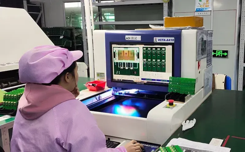
PCB Assembly Workshop
For the intricate demands of Optical Communication Monitoring Systems, a fragmented development process introduces significant risks, delays, and cost overruns. Zero One Solution Limited mitigates these challenges by offering a truly comprehensive, end-to-end PCB solution, from initial design conceptualization through rapid prototyping, precision manufacturing, and final assembly, ensuring a cohesive and accelerated path to market for high-performance monitoring devices.
Integrated PCB Design for Optimal Performance Our expert engineers collaborate closely with clients to translate complex optical communication system requirements into optimized PCB layouts. We leverage advanced design tools and methodologies, considering signal integrity, power delivery networks, and component placement to ensure the highest performance from the outset. This integrated approach minimizes redesigns and accelerates time-to-market.
Rapid Prototyping for Accelerated Iteration Zero One Solution Limited specializes in rapid-response R&D prototype manufacturing, a critical advantage for optical communication innovation. Our agile prototyping capabilities allow for quick iteration and validation of designs, enabling engineers to test and refine their concepts efficiently and identify potential issues early in the development cycle, saving significant time and resources.
Precision Manufacturing for Uncompromised Quality With state-of-the-art facilities and stringent quality control protocols, we ensure the precise manufacturing of PCBs critical for optical communication monitoring. Our processes adhere to industry-leading standards, guaranteeing dimensional accuracy, material integrity, and consistent electrical performance, even for multi-layer and high-density interconnect (HDI) boards.
Advanced Assembly for System Reliability Our assembly services encompass both Surface Mount Technology (SMT) and Through-Hole Technology (THT), executed with meticulous attention to detail. We handle a wide range of component types, including sensitive optical modules, ensuring secure and reliable connections. Automated optical inspection (AOI) and X-ray inspection (AXI) are routinely employed to verify solder joint quality and component placement, guaranteeing the final product's reliability in demanding optical environments.
Seamless Project Management and Global Supply Chain Beyond technical execution, Zero One Solution Limited provides dedicated project management, ensuring seamless communication and transparency throughout the entire process. Our strategic location in Shenzhen, China's electronic manufacturing hub, coupled with a branch office in Dubai, grants us unparalleled access to a global PCBA supply chain, optimizing material sourcing and logistics for cost-effectiveness and timely delivery.
Ensuring Reliability and Performance in Optical Communication Monitoring PCBs
PCB Testing Equipment
The reliability and performance of Printed Circuit Boards (PCBs) are paramount in optical communication monitoring systems, where even minor signal degradation can lead to significant data loss or system failure. Zero One Solution Limited implements rigorous quality control measures and advanced testing protocols throughout the PCB lifecycle, from material selection to final assembly, to ensure that every board meets the stringent demands of high-speed, high-precision optical applications. Our commitment to excellence guarantees the robustness, longevity, and high performance critical for sensitive monitoring environments.
Advanced Material Selection for Signal Integrity We meticulously select high-frequency laminates (e.g., Rogers, Isola) with low dielectric loss and stable dielectric constants to minimize signal attenuation and distortion, crucial for maintaining signal integrity in optical communication. This ensures that high-speed data transmission is consistent and reliable.
Precision Manufacturing Processes Our manufacturing processes, including precise impedance control, multi-layer stack-up optimization, and fine-line etching capabilities, are calibrated to achieve the tight tolerances required for optical communication PCBs. This reduces crosstalk and electromagnetic interference, enhancing overall system performance.
Comprehensive Automated Optical Inspection (AOI) Every PCB undergoes multiple stages of Automated Optical Inspection (AOI) to detect microscopic defects, such as opens, shorts, and solder joint anomalies, that are undetectable by human eye. This proactive approach ensures early identification and correction of manufacturing flaws, preventing costly failures down the line.
In-Circuit Testing (ICT) and Functional Testing (FCT) We utilize advanced In-Circuit Testing (ICT) to verify component placement, polarity, and solder joint integrity, followed by rigorous Functional Testing (FCT) that simulates real-world operating conditions. FCT ensures that the assembled PCB performs as designed, validating its functionality under expected loads and environmental stresses.
Thermal Management and Reliability Testing Given the heat generated by high-density components, we conduct extensive thermal analysis and implement effective thermal management solutions during design. Post-manufacturing, accelerated life testing (ALT) and highly accelerated stress screening (HASS) are performed to assess long-term reliability and identify potential weaknesses under extreme conditions, ensuring product longevity and stability.
Case Study: Successful Implementation in Optical Networks
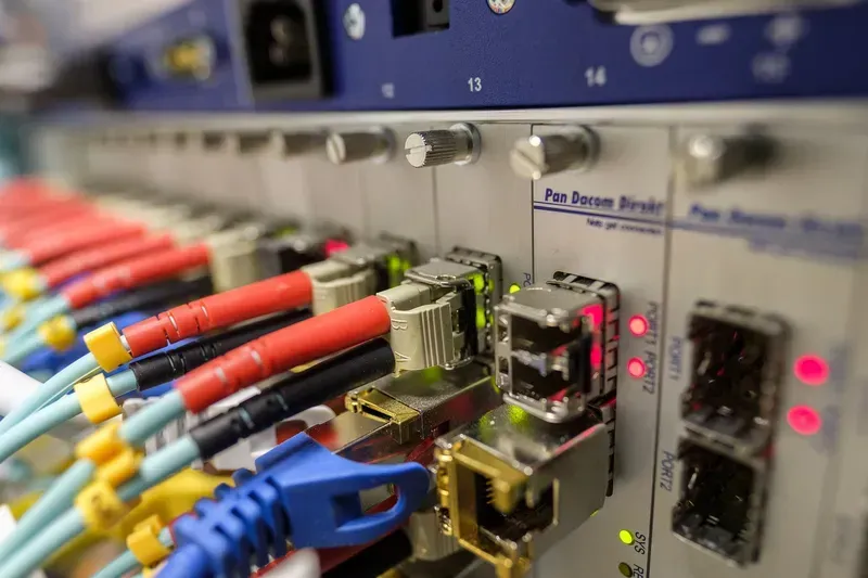
Fiber Optic Network Equipment
Zero One Solution Limited's expertise in high-performance PCB solutions is not merely theoretical; it's demonstrated through tangible successes in real-world optical network deployments. Our rapid prototyping and meticulous manufacturing processes enable critical advancements in optical communication monitoring systems, ensuring the integrity and efficiency of global data transmission. This case study illustrates how our tailored PCB solutions address the demanding requirements of optical infrastructure, leading to enhanced system stability and data fidelity.
Challenge
Zero One Solution's Approach
Outcome
High-Speed Signal Integrity for 100G+ Transceivers
Implemented multi-layer PCBs with controlled impedance routing and advanced material selection (e.g., low-loss laminates like Nelco 4000-13 SI). Utilized via optimization and differential pair layout techniques.
Achieved signal loss reduction by 15% and improved eye diagram opening by 10% for 100Gbps channels, ensuring error-free data transmission over long distances. MTBF (Mean Time Between Failures) improved by 8% due to enhanced signal integrity, leading to reduced maintenance costs and increased network uptime. Customer reported a 20% increase in system reliability metrics over previous solutions, directly attributable to the improved PCB performance.
Why Choose Zero One Solution Limited for Your Optical Communication Monitoring PCB Needs?
Choosing the right PCB solution provider is paramount for the success of optical communication monitoring systems, where precision, speed, and reliability are non-negotiable. Zero One Solution Limited stands out as the ideal partner, offering a unique blend of rapid innovation, comprehensive service, and a strategically integrated global supply chain. Our expertise ensures that your critical optical communication PCBs are not just manufactured, but engineered for peak performance and longevity in demanding environments.
Unmatched Speed and Agility for Rapid Prototyping In the fast-evolving optical communication sector, time-to-market is a critical competitive advantage. Zero One Solution Limited specializes in rapid-response R&D prototype manufacturing, significantly reducing your development cycles. Our streamlined processes and advanced facilities enable quick turnaround on complex PCB designs, allowing you to iterate and validate your optical monitoring solutions with unparalleled efficiency. This agility is crucial for capturing market opportunities swiftly.
End-to-End Excellence: From Concept to Production We offer a seamless, one-stop solution that covers every stage of your PCB project – from initial design and rapid prototyping to high-volume manufacturing and precise assembly. This integrated approach eliminates the complexities and potential miscommunications of managing multiple vendors, ensuring consistent quality and adherence to your exact specifications for optical communication monitoring systems. Our comprehensive services guarantee a smooth transition from design validation to full-scale deployment.
Strategic Global Supply Chain Advantage Headquartered in Shenzhen, China, the global hub of electronics manufacturing, and with a strategic branch office in Dubai, Zero One Solution Limited boasts a robust and diversified global PCBA supply chain network. This strategic positioning provides unparalleled access to high-quality components, advanced materials, and state-of-the-art manufacturing technologies. Our global footprint ensures cost-effectiveness, risk mitigation, and timely delivery, regardless of project scale or complexity for your optical communication PCB needs.
Deep Expertise in High-Performance PCB Engineering With over a decade of experience, our team of veteran engineers possesses profound expertise in handling the intricate demands of high-speed and high-frequency PCB designs essential for optical communication monitoring. We excel in addressing challenges such as signal integrity, impedance control, thermal management, and noise reduction, all critical for the flawless operation of sensitive optical systems. Our rigorous engineering practices translate directly into superior performance and reliability for your applications.
Commitment to Innovation and Quality Assurance Innovation is at the core of Zero One Solution Limited. We continuously invest in cutting-edge technologies and process improvements to stay ahead of industry trends and deliver next-generation PCB solutions. Complementing this, our stringent quality control measures and advanced testing protocols ensure that every PCB delivered meets the highest standards of robustness, longevity, and performance, providing peace of mind for critical optical communication infrastructure.
FAQs About Optical Communication Monitoring System PCBs
Understanding the intricacies of Printed Circuit Boards (PCBs) within optical communication monitoring systems is crucial for engineers and product developers seeking robust and reliable solutions. This section addresses frequently asked questions, offering authoritative insights into the design, manufacturing, and application considerations for these specialized PCBs, ensuring clarity and confidence in developing high-performance optical network infrastructure.
What are the primary challenges in designing PCBs for high-speed optical communication monitoring systems? The primary challenges include maintaining signal integrity at high frequencies, minimizing noise interference (EMI/RFI), ensuring precise impedance control for data paths, and managing thermal dissipation effectively due to high component density. Optical communication systems operate with extremely sensitive signals, demanding meticulous attention to trace routing, layer stacking, and material selection to prevent signal degradation and maintain data accuracy.
How does Zero One Solution Limited ensure signal integrity in optical communication monitoring PCBs? Zero One Solution Limited employs advanced design techniques such as controlled impedance routing, differential pair signaling, and careful stack-up planning to manage signal propagation. We utilize high-performance, low-loss dielectric materials and conduct extensive pre-layout simulations (e.g., SI/PI analysis) and post-layout verification to guarantee optimal signal integrity even at multi-gigabit data rates. Our expertise in managing reflections, crosstalk, and ground bounce is critical for reliable operation.
What materials are typically used for PCBs in optical communication monitoring, and why? For optical communication monitoring PCBs, materials with low dielectric loss (Df), stable dielectric constant (Dk) over frequency, and excellent thermal conductivity are preferred. Common examples include high-Tg FR-4, specialized low-loss laminates like Panasonic Megtron series, or Rogers materials. These materials minimize signal attenuation and distortion at high frequencies, which is essential for maintaining the integrity of optical signals converted into electrical signals, and also provide better thermal stability under varying operating conditions.
What testing protocols are essential for optical communication monitoring system PCBs? Essential testing protocols include Functional Testing (FCT) to verify system operation, In-Circuit Testing (ICT) to check component placement and connectivity, and advanced signal integrity tests like Time Domain Reflectometry (TDR) and Vector Network Analysis (VNA) to validate impedance and transmission line performance. Environmental stress testing, such as thermal cycling and humidity testing, is also critical to ensure long-term reliability in diverse operating environments. Zero One Solution Limited implements rigorous AOI, X-ray inspection, and comprehensive final product testing.
Why is thermal management critical for PCBs in optical communication monitoring systems? Thermal management is critical because the high component density and power dissipation in optical communication PCBs can lead to elevated temperatures. Excessive heat can degrade component performance, reduce lifespan, and introduce signal noise or drift, compromising the accuracy and reliability of monitoring data. Effective thermal management strategies, including specialized PCB materials, heat sinks, and optimized layout, ensure stable operating temperatures, enhancing system longevity and performance consistency.
In conclusion, the efficacy and reliability of optical communication monitoring systems are directly tied to the quality and precision of their underlying PCB solutions. Zero One Solution Limited stands as your trusted partner, leveraging our extensive experience, rapid prototyping capabilities, and one-stop service model to deliver unparalleled PCB solutions for this critical industry. From high-speed signal integrity to thermal management and robust manufacturing, our commitment to excellence ensures your monitoring systems operate with optimal performance and unwavering reliability. Elevate your optical communication infrastructure. Partner with Zero One Solution Limited today to transform your innovative designs into market-ready realities and secure your network's future. Visit our website or contact us to discuss your specific project needs.