In today's interconnected world, Wireless Sensor Networks (WSNs) are the backbone of countless IoT applications, from smart agriculture to industrial automation. The performance, reliability, and efficiency of a WSN node hinge critically on its Printed Circuit Board (PCB). At Zero One Solution Limited, we understand these intricate demands. With over a decade of expertise in rapid-response R&D prototype manufacturing and a global supply chain network, we specialize in delivering cutting-edge PCB solutions tailored for WSN nodes, ensuring your innovations not only come to life but thrive in the market.
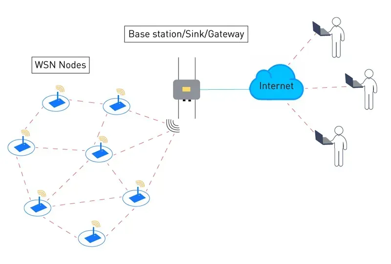
Wireless Sensor Networks (WSNs) are distributed networks comprising numerous, spatially dispersed autonomous devices called nodes, which collaboratively monitor physical or environmental conditions. These nodes, at their core, integrate sensing, computation, and communication capabilities, making the underlying Printed Circuit Board (PCB) a foundational element for their functionality, reliability, and efficient operation in diverse applications from industrial automation to smart agriculture. The effectiveness of a WSN hinges on the seamless integration of these components, where the PCB acts as the nervous system, orchestrating data acquisition, processing, and transmission, thereby enabling critical insights and automated responses.
| WSN Characteristic | Impact on PCB Design | Zero One Solution's Contribution |
|---|---|---|
| Low Power Consumption | Requires efficient component placement, power management circuitry, and material selection to minimize current leakage. | Specialized in ultra-low power PCB designs and material selection for extended battery life. |
| Compact Size | Demands high-density interconnect (HDI) and miniaturization techniques. | Expertise in multi-layer PCB design and micro-component integration for small form factors. |
| Environmental Resilience | Needs robust material selection, conformal coating, and proper thermal management. | Offers durable PCB manufacturing, advanced coatings, and rigorous testing for harsh environments. |
| Reliable Communication | Critical for signal integrity, impedance matching, and antenna integration. | Advanced RF PCB design capabilities ensuring optimal wireless performance. |
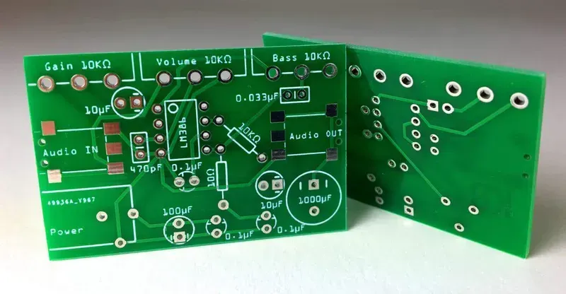
The Printed Circuit Board (PCB) is undeniably the core component of any Wireless Sensor Network (WSN) node, acting as the foundational infrastructure upon which all electronic components reside and interoperate. Its design directly dictates the node's performance, reliability, and lifespan in often challenging deployment environments. A meticulously engineered PCB ensures seamless integration of sensors, microcontrollers, and communication modules, crucially impacting signal integrity, power efficiency, and the physical footprint—factors paramount for effective WSN operation and data acquisition.
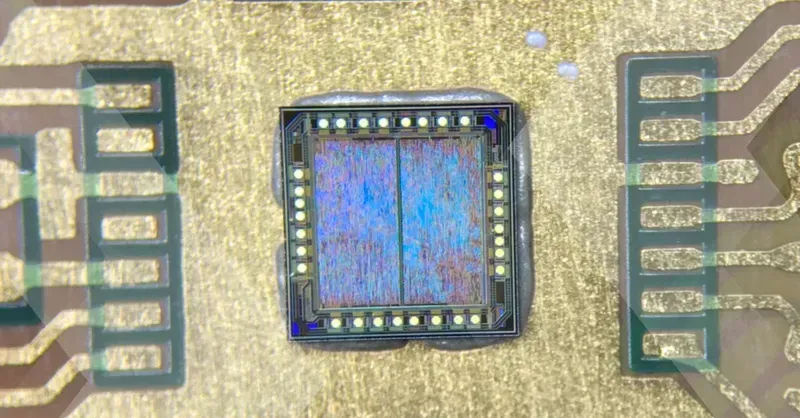
Designing Printed Circuit Boards (PCBs) for Wireless Sensor Network (WSN) nodes demands a meticulous approach, as the success and longevity of a WSN hinge significantly on the underlying hardware. The primary design considerations revolve around optimizing for low power consumption, achieving compact form factors, ensuring robust and reliable communication, and guaranteeing environmental resilience. These pillars collectively dictate the node's performance, deployment versatility, and operational lifespan, directly addressing the core pain points faced by engineers in WSN development.
| Design Aspect | Key Considerations | Impact on WSN Node |
|---|---|---|
| Low Power Consumption | Component selection (microcontrollers, transceivers), efficient power management circuits (DC-DC converters), optimized firmware operation (sleep modes) | Extends battery life, reduces maintenance, enables remote deployment |
| Compact Size | High-density component placement, multi-layer PCBs, miniature connectors, integrated modules | Facilitates discrete deployment, reduces material cost, enables application in confined spaces |
| Robust Communication | RF circuit design (impedance matching, antenna selection), interference mitigation (shielding, filtering), proper ground planes | Ensures reliable data transmission, minimizes packet loss, maintains network integrity |
| Environmental Resilience | Material selection (substrate, conformal coating), operating temperature range, vibration resistance, ingress protection (IP) rating | Guarantees long-term operation in harsh conditions, prevents premature failure, reduces replacement costs |
| Cost-Effectiveness | Standardized components, optimized manufacturing processes, scalable design for mass production | Lowers per-unit cost, accelerates market adoption, improves ROI for large deployments |
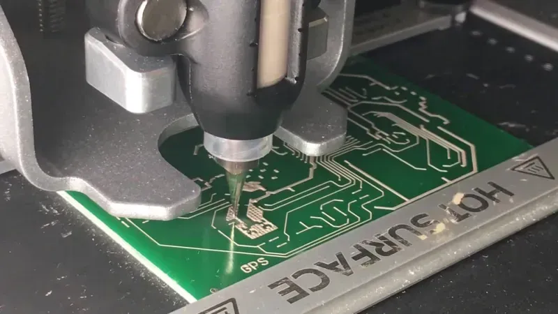
Zero One Solution Limited stands as a premier partner for Wireless Sensor Network (WSN) node PCB solutions, leveraging over a decade of specialized experience in rapid prototyping and comprehensive one-stop services. Our deep understanding of WSN-specific challenges—from ultra-low power consumption to miniaturization and ruggedization—positions us uniquely to deliver high-performance, cost-effective, and reliable PCB designs that accelerate your time to market. We are committed to empowering innovators to rapidly develop and deploy their WSN technologies with unparalleled efficiency and precision.
| Service Area | Zero One Solution's Expertise | Benefit for WSN Node PCBs |
|---|---|---|
| PCB Design & Layout | Optimized for low power, compact size, and signal integrity | Enhanced battery life and reliable data transmission |
| Component Sourcing | Global network for specialized WSN components (sensors, transceivers) | Cost-effective procurement and availability of cutting-edge technology |
| Manufacturing & Fabrication | Advanced processes for multi-layer, flexible, and HDI PCBs | Achieving high-density integration and robust physical resilience |
| Assembly (PCBA) | Precision SMT/THT assembly with stringent quality control | Reduced assembly defects and improved product reliability |
| Testing & Validation | Functional, environmental, and RF performance testing | Ensuring operational integrity in diverse WSN deployment scenarios |

Optimizing Wireless Sensor Network (WSN) node performance hinges critically on the selection of advanced technologies and materials for their Printed Circuit Boards (PCBs). Modern WSN applications demand PCBs that are not only compact and energy-efficient but also robust enough to withstand challenging environmental conditions, ensuring reliable data acquisition and transmission over extended periods. Leveraging cutting-edge materials and manufacturing processes is paramount to achieving the miniaturization, power efficiency, and signal integrity required for high-performance WSN nodes.
| Material Type | Key Advantage for WSN PCBs | Typical Application |
|---|---|---|
| Low-Loss FR-4 (e.g., Isola 370HR) | Cost-effective with improved electrical performance over standard FR-4; good thermal stability. | General purpose WSN nodes, IoT devices |
| Rogers High-Frequency Laminates (e.g., RO4000 series) | Excellent dielectric properties, low signal loss at high frequencies, good thermal management. | RF-intensive WSN nodes, radar, high-speed data transfer |
| Flexible PCB (Polyimide) | Enables compact, bendable designs for wearable WSNs or irregular form factors; excellent durability. | Wearable sensors, medical implants, curved surfaces |
| Ceramic Substrates (e.g., Alumina, LTCC) | High thermal conductivity, excellent dimensional stability, suitable for high-density integration and harsh environments. | High-power WSN nodes, automotive, aerospace applications |
Zero One Solution Limited actively integrates these advanced technologies and materials into our WSN PCB solutions. Our expertise in rapid prototyping allows us to quickly iterate on designs, experimenting with different material compositions and manufacturing techniques to achieve optimal performance for specific WSN applications. This includes sophisticated multi-layer designs, precise impedance control, and advanced thermal management strategies, ensuring that every WSN node PCB we produce meets the stringent demands of modern wireless sensor deployments.

For Wireless Sensor Network (WSN) nodes, ensuring reliability and longevity is paramount, as these devices often operate in harsh, remote, or inaccessible environments where maintenance is challenging and costly. The PCB is the fundamental backbone of a WSN node; its design, manufacturing, and the quality assurance processes directly dictate the system's resilience against environmental stressors, operational consistency, and extended lifespan. A robust PCB solution is not merely about initial functionality, but about sustaining performance over years, making rigorous testing and durable material selection critical to the success of any WSN deployment.
| Reliability Factor | Key Consideration | Impact on WSN Longevity |
|---|---|---|
| Environmental Robustness | IPC Class 2/3 standards, conformal coating, hermetic sealing | Prevents corrosion, moisture ingress, and physical damage, extending operational life in harsh conditions |
| Thermal Management | Optimized copper pour, thermal vias, heatsinks (if necessary) | Dissipates heat effectively, preventing component degradation and ensuring stable performance over time |
| Vibration & Shock Resistance | Robust mechanical design, secure component mounting, appropriate solder joint integrity | Maintains electrical connections and component functionality despite physical disturbances |
| Power Integrity | Stable voltage regulation, low ESR capacitors, efficient power pathways | Ensures consistent power delivery to all components, preventing erratic behavior and component stress |
| Material Selection | High Tg laminates, lead-free solder, durable surface finishes (ENIG, Immersion Tin) | Resists delamination, minimizes oxidation, and maintains electrical properties under stress, enhancing overall lifespan |
| Signal Integrity | Controlled impedance traces, proper grounding, minimized crosstalk | Ensures accurate data transmission, reducing errors and retransmissions, leading to more efficient and reliable network operation |
The efficacy of a Wireless Sensor Network (WSN) node is intrinsically linked to its PCB, and a one-size-fits-all approach is rarely optimal given the vast array of WSN applications. Tailored PCB solutions are paramount to achieving peak performance, ensuring long-term reliability, and cost-effectiveness across diverse deployment scenarios, from harsh industrial environments to intricate smart city infrastructures. Zero One Solution Limited specializes in providing bespoke PCB solutions that align precisely with the unique demands of each WSN application, optimizing for specific power budgets, communication protocols, sensor integrations, and environmental resilience requirements.
| WSN Application | Key PCB Customization Needs | Zero One Solution's Approach |
|---|---|---|
| Industrial IoT (IIoT) | Robustness against vibrations/temperature extremes, low power for remote deployment, EMI shielding for noisy environments. | Utilizing high-Tg laminates, advanced thermal management, and multi-layer designs with dedicated ground planes to ensure signal integrity and durability in harsh industrial settings. Integration of ruggedized connectors and protective coatings for enhanced resilience. |
| WSN Application | Key PCB Customization Needs | Zero One Solution's Approach |
|---|---|---|
| Smart Cities/Environmental Monitoring | Miniaturization for discreet placement, energy harvesting integration, long-range communication support, weatherproofing. | Employing compact, high-density interconnect (HDI) designs to fit confined spaces, incorporating power management ICs optimized for energy harvesting, and designing for RF integrity to support reliable long-range data transmission in urban landscapes. Selection of materials resistant to environmental factors. |
| WSN Application | Key PCB Customization Needs | Zero One Solution's Approach |
|---|---|---|
| Healthcare/Wearables | Ultra-miniaturization, biocompatible materials, low power for extended battery life, high signal-to-noise ratio for sensitive data. | Leveraging flexible PCBs (FPCBs) and rigid-flex designs for ergonomic and space-constrained applications. Focus on ultra-low power designs, impedance-controlled routing for high-fidelity sensor data, and selecting materials suitable for medical compliance and direct skin contact. |
| WSN Application | Key PCB Customization Needs | Zero One Solution's Approach |
|---|---|---|
| Agriculture/Precision Farming | Resistance to moisture, dust, and pesticides; wide operating temperature range; long-range, low-power communication. | Designing with conformal coatings and sealed enclosures to protect against environmental ingress. Optimizing component placement and trace routing for robust long-range wireless communication (e.g., LoRa, NB-IoT) in expansive outdoor settings, while prioritizing energy efficiency for prolonged field deployment. |
| WSN Application | Key PCB Customization Needs | Zero One Solution's Approach |
|---|---|---|
| Logistics/Asset Tracking | Compactness for integration into various assets, robust connectivity for mobile environments, long battery life. | Focusing on compact form factors and efficient power management circuits to maximize battery life. Designing for reliable cellular (e.g., LTE-M) or satellite communication modules, ensuring consistent data transmission even in challenging and dynamic environments. Emphasizing durability to withstand handling and transport stress. |
The successful deployment of Wireless Sensor Network nodes fundamentally relies on robust, efficient, and reliable PCB solutions. Zero One Solution Limited stands as your premier partner, combining deep engineering expertise with agile manufacturing capabilities to transform your WSN concepts into market-ready products. Our commitment to rapid prototyping, quality, and comprehensive support ensures that your IoT innovations are built on a solid foundation. Don't let PCB complexities slow down your progress. Partner with Zero One Solution Limited and accelerate your journey to market. Visit our website today to discuss your Wireless Sensor Network Node PCB Solution needs and discover how we can empower your next breakthrough!

