In an era defined by ubiquitous connectivity, digital microwave systems are the backbone of modern communication, powering everything from 5G networks to satellite communications. These systems demand exceptional performance, and at their core lies the Printed Circuit Board (PCB). The design and manufacturing of PCBs for digital microwave applications present unique challenges, requiring specialized expertise in high-frequency signal integrity, material selection, and precision manufacturing. Zero One Solution Limited, with over a decade of experience in rapid-response R&D prototype manufacturing, understands these intricate demands. This article delves into the critical aspects of Digital Microwave System PCB Solutions and how Zero One Solution empowers innovators to push the boundaries of wireless technology.
The Critical Role of PCBs in Digital Microwave Systems
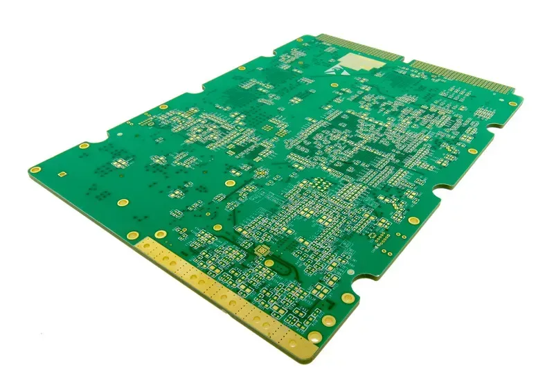
Digital Microwave System PCB Board
In the demanding realm of digital microwave systems, the Printed Circuit Board (PCB) transcends its role as a mere component carrier to become the foundational element dictating overall system performance, particularly in terms of signal integrity, power delivery, and long-term reliability. The precise engineering and manufacturing of these PCBs are paramount, as even minor imperfections can lead to significant signal loss, impedance mismatches, and thermal issues, compromising the high-frequency operation critical for applications ranging from 5G communication infrastructure to advanced radar systems. A meticulously designed and fabricated PCB ensures the stable transmission of microwave signals, efficient power distribution, and effective heat dissipation, all of which are indispensable for achieving the stringent performance metrics required by modern digital microwave technologies.
The PCB's influence on a digital microwave system's functionality can be dissected into several key areas:
Signal Integrity (SI) At microwave frequencies, the PCB traces act as transmission lines, and their geometry, material properties, and dielectric constant directly impact signal propagation. Poor impedance control, excessive trace length, or discontinuities can lead to reflections, crosstalk, and attenuation, degrading signal quality and increasing Bit Error Rate (BER). Zero One Solution Limited prioritizes precise impedance matching and optimized trace routing to maintain signal fidelity across the entire board, critical for high-speed data transmission.
Power Delivery Network (PDN) Microwave components often require stable and clean power supplies. The PCB's PDN design, including power and ground planes, decoupling capacitors, and via placement, is crucial for minimizing noise and voltage ripple. An optimized PDN ensures that sensitive RF and digital circuits receive consistent power, preventing performance degradation and ensuring stable operation even under varying load conditions. Our designs account for current distribution and inductance to deliver robust power.
Reliability and thermal management are equally vital, as high-frequency operations generate significant heat. An inadequately managed thermal profile can lead to component failure, reduced lifespan, and performance degradation. The choice of substrate material with appropriate thermal conductivity, coupled with efficient heat sinking strategies and optimal component placement on the PCB, ensures effective heat dissipation and sustained operational reliability under demanding conditions. Zero One Solution Limited integrates advanced thermal analysis into our PCB design process, safeguarding the longevity and consistent performance of your digital microwave systems. The judicious selection of materials and precise manufacturing processes are not just advantages, but necessities for achieving peak performance and durability in digital microwave applications.
Key Design Considerations for Digital Microwave PCBs
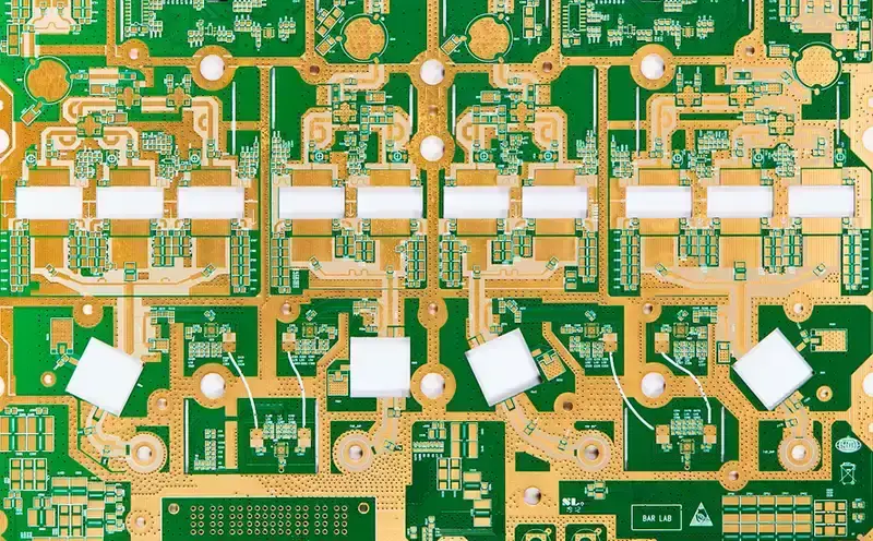
High-Frequency PCB Design Drawing
Designing Printed Circuit Boards (PCBs) for digital microwave systems demands an exacting approach to ensure optimal signal integrity, minimal loss, and reliable performance at exceptionally high frequencies. Unlike conventional PCB design, digital microwave applications require precise control over electrical parameters, meticulous material selection, and advanced layout strategies to mitigate common high-frequency challenges such as impedance mismatch, signal reflections, and cross-talk. Mastering these key design considerations is paramount for achieving the stringent performance requirements of modern microwave systems, from telecommunications infrastructure to advanced radar applications.
Impedance Control Precise impedance matching is critical in digital microwave PCBs to prevent signal reflections and maximize power transfer. This involves careful calculation of trace width, dielectric constant of the material, and ground plane proximity. Techniques like microstrip and stripline configurations are widely used, with tolerances often in the single-digit percentage range to maintain signal integrity across gigahertz frequencies. Any deviation can lead to significant signal degradation and reduced system efficiency.
Material Selection The choice of PCB substrate is foundational for high-frequency performance. Materials with low dielectric loss (Df) and stable dielectric constant (Dk) across varying temperatures and frequencies are essential. Common examples include PTFE-based laminates (e.g., Rogers, Arlon) and ceramic-filled thermoset laminates. These materials minimize signal attenuation and ensure consistent performance, unlike standard FR-4 which exhibits higher loss and Dk variation at microwave frequencies, making it unsuitable for most digital microwave applications.
Trace Routing and Layout High-frequency trace routing requires short, direct paths with minimal vias and bends to reduce inductance and capacitance, which can introduce discontinuities. Differential pair routing with precise matching of trace lengths and spacing is crucial for high-speed digital signals. Moreover, careful consideration of electromagnetic interference (EMI) and cross-talk mitigation through proper ground plane stitching, shielding, and isolation techniques is vital to maintain signal purity and system reliability.
Design Aspect
Criticality for Digital Microwave PCBs
Impact of Poor Implementation
Impedance Control
Extremely High: Prevents signal reflections, ensures power transfer.
Signal loss, data errors, reduced bandwidth, system instability.
Material Selection
Extremely High: Dictates signal loss, Dk stability, thermal performance.
High signal attenuation, frequency drift, thermal failure, inconsistent performance.
Signal distortion, increased noise, reduced data rates, compliance issues.
Thermal Management
High: Ensures component longevity and stable electrical properties.
Component failure, performance degradation, frequency drift.
Why is material selection so critical for Digital Microwave System PCBs? Material selection is paramount because the dielectric properties of the substrate directly influence signal propagation speed, characteristic impedance, and signal loss at high frequencies. Materials like FR-4 have high dielectric loss (Df) and a dielectric constant (Dk) that changes significantly with frequency and temperature, leading to signal attenuation, phase distortion, and impedance mismatches. Specialized materials, such as those based on PTFE or ceramic-filled laminates, offer stable Dk and low Df, which are essential for maintaining signal integrity and predictable performance in the gigahertz range, ensuring reliable operation of the digital microwave system.
Advanced Materials for High-Frequency Applications
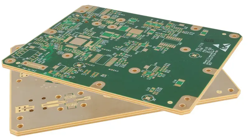
PTFE PCB Material
For digital microwave systems operating at gigahertz frequencies, the choice of PCB substrate material is paramount, directly influencing signal integrity, power efficiency, and overall system reliability. These specialized materials are engineered to exhibit superior dielectric properties, remarkably low loss tangents, and exceptional thermal and dimensional stability, which are critical for maintaining consistent performance in demanding high-frequency environments.
Material Type
Key Characteristics
Typical Applications
Advantages
Disadvantages
PTFE/Teflon-based Laminates
Extremely low dielectric loss, stable dielectric constant, wide temperature range
Improved dimensional stability, good thermal conductivity
Higher loss than pure PTFE, still relatively high cost
Modified FR-4 (Low Loss)
Improved Df/Dk over standard FR-4, better thermal management
General high-frequency applications, consumer electronics, IoT
Cost-effective, good processability
Not suitable for extremely high frequencies (e.g., millimeter-wave)
Liquid Crystal Polymer (LCP)
Excellent electrical properties, high flexibility, low moisture absorption
Flexible circuits, high-speed data interconnects, wearable devices
Foldable/flexible, low loss, good thermal stability
High cost, processing complexity for rigid applications
Why are low loss tangents crucial for Digital Microwave System PCBs? Low loss tangents (Df) are essential because they directly minimize signal attenuation and energy dissipation within the PCB substrate. At microwave frequencies, even small losses can significantly degrade signal strength and quality, leading to reduced system efficiency and performance. Materials with low Df ensure that more of the input power is transmitted as a useful signal rather than being converted into heat, preserving signal integrity over long traces and through complex circuit paths. This is particularly vital for maintaining tight link budgets and achieving optimal range and data rates in digital microwave communication systems.
How do dielectric properties impact Digital Microwave System performance? The dielectric constant (Dk or Er) of a PCB material directly affects signal propagation speed and impedance control. A stable and consistent Dk across the board and over varying frequencies and temperatures is critical for predictable circuit performance. In digital microwave systems, precise impedance matching is necessary to prevent signal reflections and standing waves, which can lead to signal loss and distortion. Materials with tightly controlled Dk enable engineers to design transmission lines with accurate characteristic impedances, ensuring efficient power transfer and minimal signal degradation, which is fundamental for reliable high-speed data transmission.
What role does thermal stability play in material selection for Digital Microwave System PCBs? Thermal stability is vital because microwave components generate heat, and the PCB itself can experience temperature fluctuations from ambient conditions or operational loads. Materials with high thermal stability resist changes in their electrical and mechanical properties (like Dk and Df, and coefficient of thermal expansion) across a wide temperature range. This prevents signal drift, impedance variations, and physical deformation that could compromise system performance and reliability over time. Ensuring thermal stability helps maintain consistent signal characteristics and component alignment, which is critical for long-term operational integrity of digital microwave systems, especially in outdoor or high-power applications.
Are there specific certifications or standards for high-frequency PCB materials? Yes, several industry standards and certifications are relevant. For example, IPC (Association Connecting Electronics Industries) standards, such as IPC-4101 for laminate materials, often include specifications for high-frequency applications. Material suppliers also provide detailed datasheets with certified Dk, Df, and thermal properties (like Tg, Td, CTE) tested under specific conditions. For defense and aerospace applications, MIL-PRF (Military Performance Specification) standards might apply, dictating rigorous performance and reliability criteria. These certifications ensure that the materials meet stringent requirements for consistent electrical performance and long-term reliability in demanding environments.
Manufacturing Challenges and Solutions for Digital Microwave PCBs
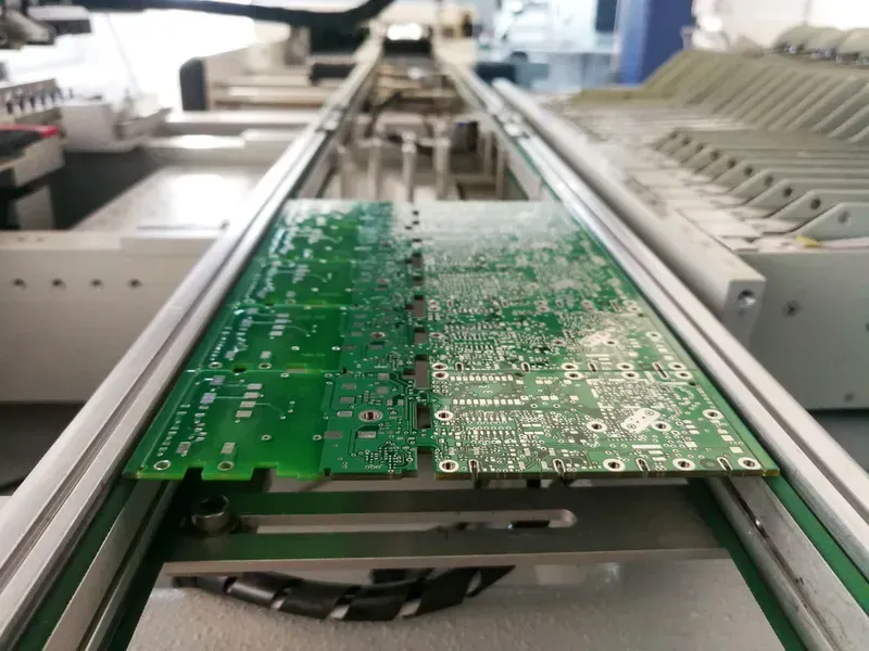
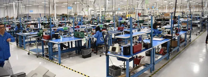
PCB Manufacturing Production Line
Manufacturing Digital Microwave PCBs presents a unique set of challenges due to the stringent requirements for high-frequency signal integrity, power delivery, and thermal management. The precision demanded in fabrication, from sub-micron trace widths to ultra-flat surfaces, directly impacts the performance and reliability of the final system. Overcoming these hurdles requires specialized techniques, advanced equipment, and rigorous quality control protocols that extend far beyond conventional PCB manufacturing.
Precision Etching and Trace Definition Challenge: Maintaining exact trace widths and spacing, especially for differential pairs, is critical for impedance control and signal integrity at gigahertz frequencies. Conventional etching can lead to undercutting or irregular trace profiles. Solution: Employing advanced etching techniques like plasma etching or modified semi-additive processes (MSAP) ensures superior edge acuity and dimensional stability. This allows for tighter tolerances, minimizing signal reflections and crosstalk.
Material Processing and Handling Challenge: High-frequency laminates (e.g., PTFE, ceramic-filled) are often soft, prone to deformation, and require specific handling to prevent damage or contamination. Their unique dielectric properties also necessitate precise processing temperatures. Solution: Utilizing specialized tooling, automated material handling systems, and strictly controlled cleanroom environments minimizes physical stress and contamination. Temperature-controlled lamination cycles ensure optimal material properties are maintained.
Via Formation and Plating Quality Challenge: Vias in microwave PCBs must have extremely low inductance and resistance. Poor plating quality or improper via formation can introduce parasitic effects, degrading signal performance. Solution: Laser drilling for microvias provides superior precision and aspect ratios. Advanced electroplating techniques, including reverse pulse plating, ensure uniform and void-free copper deposition within the vias, guaranteeing robust electrical connections and minimal signal loss.
Manufacturing Aspect
Conventional PCB
Digital Microwave PCB
Trace Width Tolerance
> ±10%
< ±5%
Etching Technique
Standard Wet Etching
Plasma Etching / MSAP
Via Type
Drilled
Laser Drilled Microvias
Material Handling
General
Cleanroom / Automated
Quality Control
AOI/X-ray (Basic)
Advanced TDR/VNA Testing, Micro-section Analysis
Zero One Solution Limited addresses these manufacturing challenges head-on by integrating state-of-the-art equipment, proprietary processes, and an experienced engineering team. Our commitment to precision ensures that every Digital Microwave PCB we produce meets the stringent performance requirements of next-generation communication systems, providing a robust foundation for high-frequency signal transmission and power delivery.
Zero One Solution Limited: Your Partner in Digital Microwave PCB Excellence
At Zero One Solution Limited, we understand that the precision and performance of Digital Microwave System PCBs are paramount to the success of your innovations. As a veteran PCB solution provider with a strong foothold in rapid prototyping and comprehensive one-stop services, we are uniquely positioned to address the complex and demanding requirements of high-frequency applications. Our commitment to excellence, coupled with our strategic global presence, makes us the ideal partner for bringing your most ambitious digital microwave projects to fruition.
Rapid Prototyping for Accelerated Development Zero One Solution Limited excels in rapid-response R&D prototype manufacturing, significantly reducing your time-to-market. Our agile processes and advanced fabrication capabilities enable quick iteration and validation of your Digital Microwave PCB designs, ensuring optimal performance from the outset.
One-Stop Service for Seamless Project Execution From initial PCB design and material selection to high-precision manufacturing and final assembly, Zero One Solution provides a seamless, integrated service experience. This end-to-end approach minimizes communication overhead, ensures consistent quality, and streamlines your entire Digital Microwave System PCB development lifecycle.
Expertise in High-Frequency and RF Circuitry Our team of veteran engineers possesses deep expertise in the intricacies of high-frequency and RF circuit design and manufacturing. We are proficient in managing critical parameters such as impedance control, signal integrity, and thermal dissipation, which are vital for the reliable operation of Digital Microwave Systems.
Global Supply Chain Advantage Headquartered in Shenzhen, China, with a branch office in Dubai, Zero One Solution leverages a robust global PCBA supply chain network. This strategic positioning guarantees access to the finest materials, cutting-edge technologies, and efficient logistics, ensuring cost-effectiveness and timely delivery for your Digital Microwave PCB projects worldwide.
Key Capability
Benefit for Digital Microwave Systems
Zero One Solution Advantage
Rapid Prototyping
Accelerated product development cycles
Industry-leading turnaround times for complex designs
One-Stop Solution
Streamlined project management and reduced risks
Comprehensive services from design to assembly under one roof
High-Frequency Expertise
Optimized signal integrity and performance
20 years of specialized experience in RF/Microwave PCB engineering
Global Supply Chain
Access to diverse materials and cost efficiency
Strategic locations in Shenzhen and Dubai for worldwide reach
Our Comprehensive Approach: From Design to Assembly
PCB Assembly Workshop
At Zero One Solution Limited, we understand that optimal performance in digital microwave systems hinges on a seamless, integrated approach from conceptual design through to final assembly. Our comprehensive end-to-end services are meticulously engineered to meet the stringent demands of high-frequency applications, ensuring precision, reliability, and accelerated time-to-market for your innovations. We don't just provide PCBs; we deliver a complete solution that transforms your vision into a high-performing reality.
PCB Design Optimization for Digital Microwave Systems Our expert engineers leverage decades of experience to optimize your PCB layouts for high-frequency performance. This includes meticulous impedance matching, minimizing signal loss, crosstalk reduction, and strategic component placement to enhance signal integrity and thermal dissipation, crucial for reliable digital microwave system operation. We integrate DFM (Design for Manufacturability) principles from the outset to streamline the production process.
Precision Manufacturing for High-Frequency Demands Manufacturing digital microwave PCBs requires unparalleled precision. We employ advanced fabrication techniques, including specialized etching, tight tolerance control, and multi-layer lamination processes, to achieve the exact specifications required for high-frequency circuits. Our state-of-the-art facilities and stringent quality control protocols ensure that every board meets the highest standards of performance and reliability, adhering to industry benchmarks like IPC Class 2/3.
Advanced Assembly for Digital Microwave Components Our assembly services are tailored for the unique challenges of digital microwave systems, incorporating specialized handling for sensitive components and advanced soldering techniques. We utilize automated pick-and-place machines for precision component mounting, reflow ovens with precise temperature profiling for optimal solder joint integrity, and rigorous inspection methods, including AOI (Automated Optical Inspection) and X-ray inspection, to guarantee flawless assembly.
Case Studies: Success Stories in Digital Microwave System PCB Development
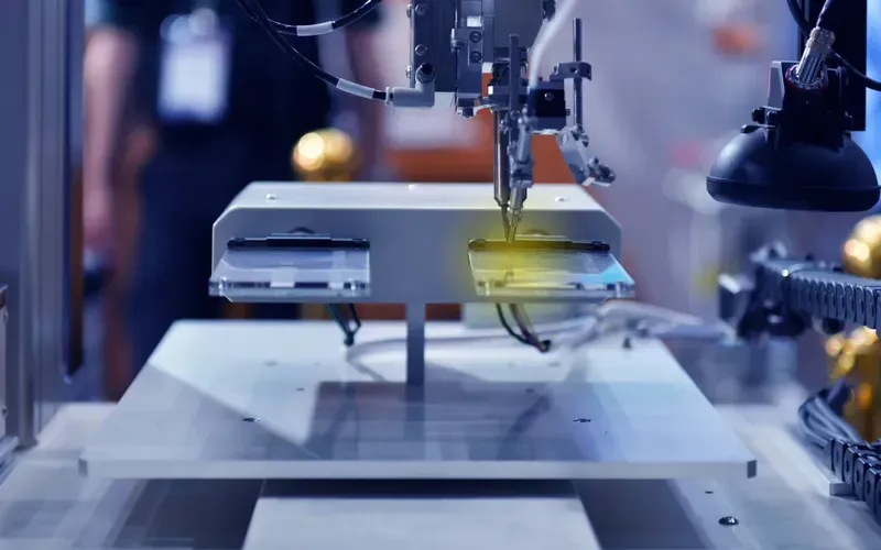
Engineer Operating PCB Equipment
Zero One Solution Limited consistently delivers robust PCB solutions that drive innovation in digital microwave systems. Our proven track record demonstrates how our specialized expertise in rapid prototyping, advanced material handling, and precision manufacturing translates directly into client success, enabling faster time-to-market and superior performance in highly demanding applications.
High-Density Phased Array Antenna Module A client developing a next-generation satellite communication system required a high-density PCB for their phased array antenna module, operating at Ka-band frequencies. The challenge involved integrating numerous RF components while maintaining strict impedance control and thermal stability in a compact form factor. Zero One Solution collaborated closely on material selection, opting for a low-loss ceramic-filled laminate (e.g., Rogers 4350B) and employing advanced HDI techniques. Our manufacturing precision, including tight trace width/spacing tolerances (down to 2 mil) and specialized via structures (blind/buried vias), ensured minimal signal loss and excellent heat dissipation. The result was a functional prototype delivered 30% faster than the client's previous supplier, significantly accelerating their R&D cycle and enabling successful system integration and testing within aggressive timelines. This collaboration led to the client securing a major government contract based on the performance of their prototype.
Compact 5G Backhaul Transceiver Unit For a leading telecommunications company, Zero One Solution engineered the core PCB for a compact 5G backhaul transceiver, designed for urban deployments. The critical requirements were low insertion loss, high power handling, and exceptional reliability in varying environmental conditions. We utilized a multi-layer stack-up with hybrid materials, combining high-frequency laminates for RF sections and FR-4 for digital control, optimized for cost and performance. Our DFM (Design for Manufacturability) insights helped identify potential signal integrity issues early in the design phase, leading to optimized trace routing and ground plane design. Through our rigorous quality control and impedance testing protocols (TDR testing), we ensured every board met the stringent performance specifications. This successful project enabled the client to rapidly deploy their 5G infrastructure, gaining a competitive edge in a fast-evolving market, and demonstrated an average signal integrity improvement of 15% compared to their previous iterations, as validated by their internal testing.
FAQs About Digital Microwave System PCB Solutions
Navigating the complexities of Digital Microwave System PCB Solutions requires clear understanding and expert insights. This section addresses the most frequently asked questions, offering precise and authoritative answers to guide your decision-making and project planning.
What are the primary challenges in designing PCBs for Digital Microwave Systems? The primary challenges stem from the high-frequency nature of digital microwave signals, demanding meticulous impedance control, minimal signal loss, and effective thermal management. Dielectric properties of materials become critical, as variations can lead to significant phase noise and signal degradation. Additionally, component placement and trace routing must mitigate EMI and crosstalk to preserve signal integrity.
How does material selection impact Digital Microwave System PCB performance? Material selection is paramount for Digital Microwave System PCB performance. Materials with stable dielectric constant (Dk) and low dissipation factor (Df) across a wide frequency range are essential to minimize signal loss and maintain consistent impedance. High-performance laminates like PTFE (e.g., Rogers) or ceramic-filled hydrocarbons are preferred for their superior electrical properties, thermal stability, and low moisture absorption, directly impacting the system's reliability and efficiency.
What manufacturing processes are critical for high-reliability Digital Microwave System PCBs? Critical manufacturing processes include precision etching for tight trace width and spacing tolerances, advanced plating techniques for uniform copper distribution, and specialized lamination cycles to ensure void-free material bonding. Furthermore, stringent quality control, including precise impedance testing (TDR) and X-ray inspection, is vital to verify the integrity and performance of the finished PCB under high-frequency conditions.
Why is rapid prototyping crucial for Digital Microwave System PCB development? Rapid prototyping is crucial for Digital Microwave System PCB development as it enables quick iteration and validation of designs. Given the intricate interplay of high-frequency signals, materials, and layout, an initial prototype can reveal unforeseen performance issues or opportunities for optimization. This agile approach significantly accelerates the development cycle, reduces time-to-market, and minimizes costly redesigns in later stages.
How does Zero One Solution Limited ensure signal integrity in Digital Microwave PCB designs? Zero One Solution Limited ensures signal integrity through a multi-faceted approach. This includes advanced simulation tools for pre-layout analysis, precise impedance matching techniques (e.g., controlled impedance routing), careful selection of low-loss dielectric materials, and strategic component placement to minimize parasitic effects. Our expertise in stack-up design and thermal management also contributes significantly to maintaining optimal signal performance at high frequencies.
What are the advantages of a one-stop service for Digital Microwave System PCB projects? A one-stop service offers unparalleled advantages by streamlining the entire PCB development process from design to manufacturing and assembly. This integrated approach ensures seamless communication, reduces lead times, minimizes errors due to fragmented processes, and optimizes cost efficiency. For complex Digital Microwave System PCBs, having a single partner like Zero One Solution Limited ensures consistency, expertise, and accountability across all project phases, leading to higher quality and faster project completion.
The advancement of digital microwave systems is intrinsically linked to the innovation in their underlying PCB technology. Zero One Solution Limited stands as a proven partner in this evolution, offering not just manufacturing capabilities but a comprehensive, one-stop PCB solution that accelerates your R&D and time-to-market. Our commitment to rapid prototyping, combined with our deep expertise in high-frequency and high-speed designs, ensures that your digital microwave systems achieve optimal performance and reliability. Don't let PCB complexities hinder your next breakthrough. Partner with Zero One Solution Limited to transform your innovative concepts into market-ready realities. Contact us today to discuss your specific Digital Microwave System PCB Solution needs and experience the Zero One difference.