In the rapidly evolving landscape of telecommunications, Massive Multiple-Input Multiple-Output (MIMO) technology stands as a cornerstone for unlocking the full potential of 5G and beyond. This paradigm shift in wireless communication, enabling unprecedented data rates and network capacity, places immense demands on the underlying hardware – particularly the Radio Frequency (RF) board. At Zero One Solution Limited, a leader in advanced PCB solutions with a decade of expertise, we understand these critical requirements. This article delves into the complexities and crucial considerations for developing robust Massive MIMO RF board solutions, highlighting how our rapid-response R&D prototype manufacturing and one-stop services empower innovators to accelerate their product development cycle and bring cutting-edge solutions to market with unmatched efficiency.
Understanding Massive MIMO: The Foundation of Next-Gen Wireless
Massive MIMO (Multiple-Input Multiple-Output) stands as a cornerstone of 5G and future wireless communication systems, revolutionizing network capacity, spectral efficiency, and reliability. By employing a large number of antennas at the base station, Massive MIMO fundamentally transforms how data is transmitted and received, enabling unprecedented gains in user experience and network performance, which directly impacts the stringent requirements for advanced RF board solutions. This technology is critical for supporting the vast data demands of modern applications, from high-definition streaming to the Internet of Things (IoT).
What is the core principle of Massive MIMO? Massive MIMO's core principle involves deploying a significantly larger number of antennas at the base station compared to traditional MIMO systems. These antennas simultaneously serve multiple users, employing advanced signal processing techniques like spatial multiplexing and beamforming to direct focused energy towards individual users. This drastically reduces interference and enhances signal quality, maximizing data throughput and connectivity for numerous devices within the same cell. The ability to manage a multitude of spatially separated data streams is paramount to its effectiveness, demanding highly precise RF front-end designs and advanced antenna array integration on the RF board itself. This approach shifts the paradigm from simply transmitting more power to intelligently shaping radio waves for optimal delivery, a capability dependent on the underlying RF board's ability to handle complex phase and amplitude control across a multitude of channels reliably and efficiently, leading to enhanced spectral efficiency and reduced inter-user interference. The sheer number of antenna elements and the need for tight phase coherence across them place significant demands on the RF board's design and manufacturing precision. Each antenna path, comprising RF chains, phase shifters, and amplifiers, must be meticulously engineered to maintain signal integrity and minimize losses, especially at higher frequencies.
Feature
Traditional MIMO
Massive MIMO
Antenna Count
2-8
64-256+
Spectral Efficiency
Good
Excellent (5-10x improvement)
Capacity
Moderate
High (Scalable with users)
Interference Management
Limited
Superior (Advanced beamforming)
Reliability
Good
Enhanced (Spatial diversity)
Energy Efficiency
Standard
Improved (Reduced transmit power per user)
How does Massive MIMO enhance spectral efficiency and capacity? Massive MIMO significantly boosts spectral efficiency by enabling multiple users to share the same time and frequency resources through spatial multiplexing. By simultaneously serving numerous users with distinct data streams, and using precise beamforming to direct signals specifically to each user while nulling out interference for others, it effectively reuses spectrum multiple times within the same cell. This spatial separation of users leads to a substantial increase in system capacity, allowing more data to be transmitted over a given bandwidth, a crucial advantage for accommodating the ever-growing data demands of 5G networks and beyond. This capability is fundamentally enabled by RF board designs that can manage a high density of parallel RF chains with minimal cross-talk and excellent phase coherence across all channels.
Critical Challenges in Massive MIMO RF Board Design
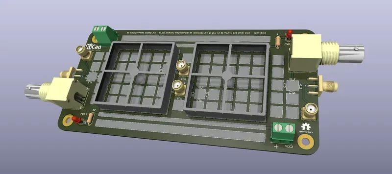
Massive MIMO RF Board Design
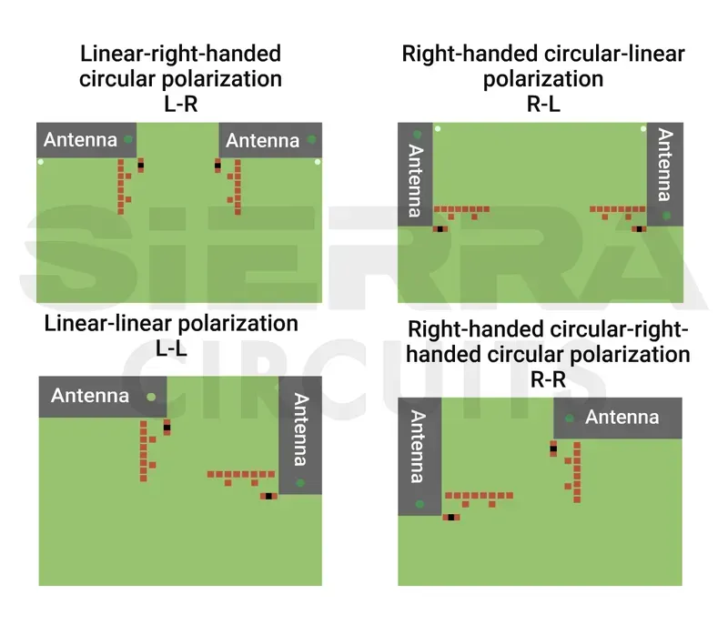
Designing Massive MIMO RF boards presents a formidable array of engineering challenges, primarily due to the technology's demanding requirements for high-frequency performance, spatial multiplexing, and vast antenna arrays. The precision needed in every aspect, from material selection to layout, is paramount for achieving the optimal performance critical for next-generation wireless communications.
Signal Integrity (SI) and Electromagnetic Interference (EMI) Maintaining pristine signal integrity across numerous RF paths is a core challenge. The dense integration of antennas and RF chains within Massive MIMO systems significantly increases the risk of crosstalk, impedance mismatches, and electromagnetic interference, which can degrade signal quality and reduce overall system efficiency. Meticulous trace routing, controlled impedance techniques, and robust shielding are essential to mitigate these issues.
Advanced Power Management Massive MIMO boards typically integrate a large number of power amplifiers (PAs), which are significant power consumers and heat generators. Efficient power delivery networks (PDNs) are crucial to ensure stable voltage supply to all active components while minimizing power loss. This involves careful consideration of DC-DC conversion, voltage regulation modules (VRMs), and power filtering to prevent noise propagation across sensitive RF circuits.
Thermal Dissipation Strategies The high power consumption of numerous RF components, particularly PAs, leads to substantial heat generation. Effective thermal management is vital to prevent performance degradation, ensure long-term reliability, and avoid component failure. This necessitates innovative thermal dissipation solutions, including the use of high-thermal-conductivity materials, optimized heat sink designs, and advanced cooling techniques within compact board footprints.
Miniaturization and High-Density Integration To enable deployment in diverse environments, Massive MIMO RF boards must be increasingly compact while accommodating a large number of antennas and complex circuitry. This demands high-density interconnect (HDI) PCB technologies, fine-pitch component placement, and multi-layer board designs, pushing the boundaries of manufacturing precision and assembly capabilities.
High-Frequency Performance and Material Selection Operating at higher frequency bands (e.g., sub-6 GHz and mmWave) introduces challenges related to dielectric loss, skin effect, and signal attenuation. Selecting appropriate low-loss dielectric materials (e.g., Rogers, PTFE-based laminates) and implementing precise fabrication processes are critical to ensure minimal signal degradation and optimal performance at these elevated frequencies.
RF Board Layout and Routing Precision The intricate nature of Massive MIMO RF boards requires exceptionally precise layout and routing. Every trace length, spacing, and bend can impact RF performance. Designers must meticulously manage impedance, minimize stub effects, and ensure proper ground planes to maintain signal integrity and prevent unwanted reflections, which are amplified in multi-antenna systems.
Key Technologies for High-Performance RF Boards
Advanced RF Board Substrate Materials
Achieving optimal performance in Massive MIMO RF boards hinges on the strategic application of cutting-edge technologies and specialized materials. These boards operate at frequencies where even minor design and material imperfections can lead to significant signal degradation, demanding a meticulously engineered approach to ensure robust and reliable wireless communication. The selection of advanced substrate materials, precise impedance control, and innovative shielding are paramount to managing the intricate interplay of high-frequency signals and minimizing interference.
Advanced Substrate Materials for Massive MIMO RF Boards The foundation of any high-performance RF board is its substrate. For Massive MIMO applications, conventional FR-4 materials often fall short due to their higher dielectric loss and inconsistent dielectric constant at high frequencies. We utilize advanced materials like Rogers (e.g., RO4000 series, RO3000 series) and PTFE (Teflon) laminates. These materials offer superior low-loss characteristics, stable dielectric constants across a wide temperature range, and excellent dimensional stability, which are critical for maintaining signal integrity and impedance matching in high-frequency circuits. For instance, Rogers 4350B provides an excellent balance of electrical performance and manufacturability, making it ideal for cost-effective high-volume production of Massive MIMO RF boards.
Precision Impedance Control in RF PCB Designs Impedance control is non-negotiable for high-frequency RF boards. Any mismatch can lead to signal reflections, power loss, and degraded performance. Our process involves precise control over trace width, spacing, and dielectric thickness to ensure the characteristic impedance of transmission lines (e.g., 50 Ohm or 75 Ohm) is maintained within tight tolerances. We leverage advanced simulation tools (e.g., Ansys HFSS, Keysight ADS) during the design phase and employ Time Domain Reflectometry (TDR) for post-manufacturing verification. This meticulous approach guarantees optimal signal propagation and minimizes return loss, crucial for the numerous antenna elements in Massive MIMO systems.
Strategic High-Frequency Component Selection and Placement The choice of components profoundly impacts RF board performance. For Massive MIMO, this includes high-linearity low-noise amplifiers (LNAs), power amplifiers (PAs), phase shifters, filters, and high-speed analog-to-digital converters (ADCs)/digital-to-analog converters (DACs). We meticulously select components with excellent RF characteristics, low parasitic inductance/capacitance, and appropriate power handling capabilities. Furthermore, component placement is optimized to minimize trace lengths, reduce coupling, and ensure efficient thermal dissipation, which is vital given the high component density on Massive MIMO boards.
Innovative Shielding Techniques for Interference Mitigation With high component density and multiple RF chains, electromagnetic interference (EMI) and crosstalk are significant concerns. We employ various shielding techniques to isolate sensitive RF circuitry and prevent interference. This includes the use of grounded guard traces, via stitching, compartmentalization with metallic fences (Faraday cages), and selective application of EMI shielding materials. These measures ensure that each RF chain operates optimally without adverse effects from adjacent circuits, maintaining the high signal-to-noise ratio required for Massive MIMO's advanced signal processing capabilities.
Advanced Manufacturing Processes for RF Board Solutions The manufacturing process itself must support the stringent requirements of Massive MIMO RF boards. This includes precise etching capabilities to achieve fine line widths and spacing, multi-layer stack-up optimization to manage impedance and crosstalk, and advanced plating techniques for robust via connections. Our state-of-the-art facilities and experienced technicians ensure that the theoretical design integrity is translated into physical reality with exceptional precision, enabling the complex interconnections and controlled impedances essential for high-performance RF boards.
Zero One Solution Limited's Expertise in RF Board Prototyping
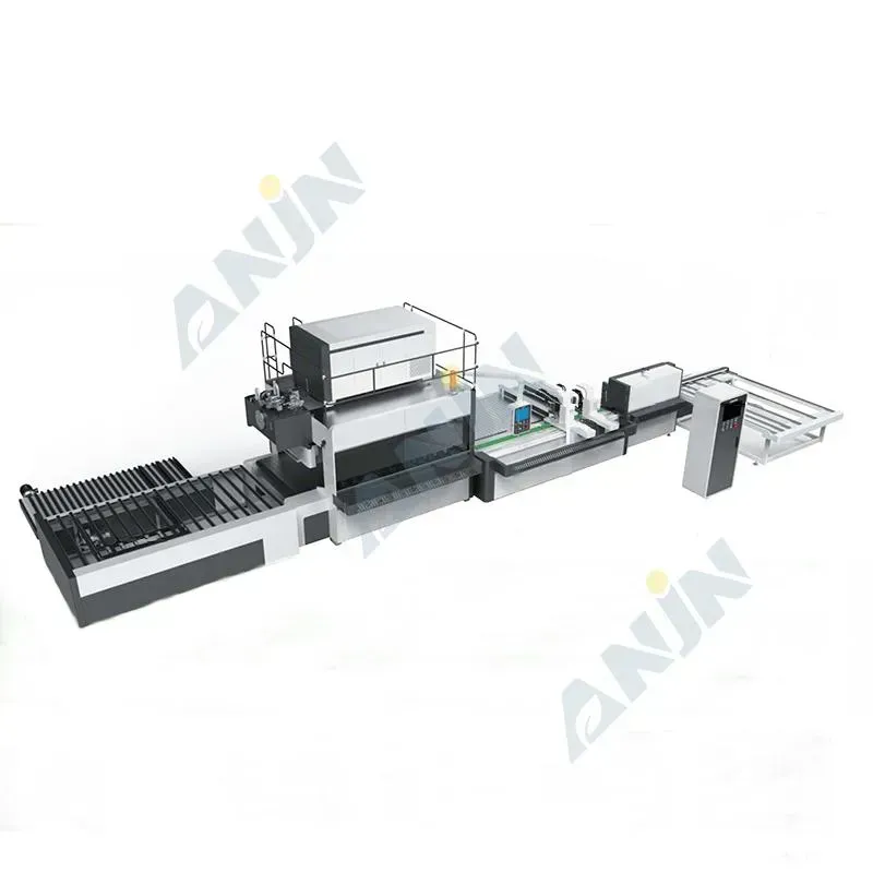
RF Board Prototyping Equipment
Zero One Solution Limited stands at the forefront of rapid prototyping for Massive MIMO RF boards, a critical enabler for accelerating innovation in 5G and next-generation wireless technologies. Our specialized expertise in this demanding field ensures that R&D cycles are significantly shortened, allowing clients to validate designs and bring cutting-edge products to market with unparalleled speed and precision. We combine agile processes, state-of-the-art equipment, and a highly experienced engineering team to address the intricate requirements of high-frequency and complex RF board prototypes, making us an indispensable partner in the evolution of wireless communication.
Agile Prototyping Processes Our rapid prototyping workflow is meticulously designed for efficiency and flexibility, allowing for quick iterations and adjustments based on design feedback. This agile methodology minimizes lead times, crucial for the fast-paced development cycles of Massive MIMO RF boards. We prioritize parallel design and manufacturing stages to streamline the entire prototyping process from concept to tangible board.
Specialized Equipment and Facilities We leverage advanced manufacturing equipment specifically calibrated for high-frequency RF board production. This includes precision etching machines, high-resolution direct imaging systems, and specialized lamination presses capable of handling diverse RF materials like Rogers and Teflon. Our facilities are optimized to maintain stringent environmental controls, critical for the integrity of high-performance RF circuits.
Capability
Impact on Massive MIMO Prototyping
Zero One Solution Limited Advantage
High-Frequency Material Handling
Ensures signal integrity and low loss at millimeter-wave frequencies.
Expertise in diverse RF laminates (e.g., Rogers, Taconic) with precise processing capabilities and a global supply chain to maintain resource access and support.
Advanced Impedance Control
Maintains consistent signal characteristics crucial for multi-antenna arrays.
Precise impedance matching down to ±5% tolerance, verified with TDR testing for optimal RF performance.
Thermal Management Solutions
Prevents performance degradation due to heat in high-power RF systems.
Integrated thermal vias, heat sinks, and material selection for efficient heat dissipation, extending component lifespan and stability.
Miniaturization & High Density
Enables compact designs for Massive MIMO arrays with thousands of elements.
Fine line/space capabilities (down to 2/2 mil), microvias, and HDI technology for maximizing component density.
What makes Massive MIMO RF board prototyping particularly challenging? The primary challenges stem from operating at higher frequencies, managing immense data throughput from numerous antennas, maintaining signal integrity across complex multi-layer structures, and effective thermal dissipation. Miniaturization, stringent impedance control, and selecting appropriate low-loss dielectric materials are also critical for achieving optimal performance in these high-density, high-frequency environments. Our solutions specifically address these challenges through advanced material expertise and precision manufacturing.
From Design to Assembly: Our One-Stop Solution for Massive MIMO RF Boards
RF Board Production Line
At Zero One Solution Limited, we understand that accelerating the development of Massive MIMO RF boards requires more than just individual services; it demands a unified, end-to-end approach. Our one-stop solution streamlines the entire production lifecycle, from initial concept design to final assembly, ensuring unparalleled efficiency, consistent quality, and a faster time-to-market for your cutting-edge wireless communication systems. This integrated methodology is particularly critical for complex high-frequency PCB boards and RF circuits where precision and seamless transitions between stages are paramount.
Professional PCB Design for Massive MIMO RF Boards Our expert design team specializes in high-frequency and RF layouts, utilizing advanced EDA tools to optimize for signal integrity, impedance control, thermal management, and miniaturization. We meticulously adhere to specifications critical for Massive MIMO, including antenna array integration, RF trace routing, and power distribution network (PDN) design, ensuring your board's foundational integrity.
Precision Manufacturing of Massive MIMO RF Boards Leveraging state-of-the-art manufacturing facilities, we produce high-precision PCBs tailored for Massive MIMO applications. This includes specialized material handling (e.g., Rogers, Taconic), advanced drilling techniques, and precise etching processes to meet tight tolerances required for high-frequency performance. Our manufacturing processes are optimized for complex multi-layer boards and intricate RF circuit fabrication.
Advanced Assembly Capabilities for Massive MIMO RF Boards Our assembly lines are equipped for high-density, fine-pitch component placement, crucial for Massive MIMO's compact designs. We employ automated SMT and through-hole processes, advanced reflow soldering, and meticulous post-assembly inspection including X-ray and AOI to ensure every component is accurately placed and securely connected. Our expertise extends to integrating RF shielding and specialized connectors essential for optimal RF performance.
Integrated Supply Chain Management Zero One Solution Limited manages the entire supply chain, from sourcing high-quality, specialized components for RF applications to managing logistics, reducing lead times, and mitigating supply chain risks. This comprehensive approach ensures that all materials meet the stringent requirements of Massive MIMO RF boards, from active RF components to passive filters and connectors.
Dedicated Project Management Each Massive MIMO RF board project benefits from dedicated project management, providing a single point of contact and ensuring seamless communication and coordination across all stages—from design review and DFM analysis to manufacturing updates and final delivery. This integrated oversight guarantees project milestones are met efficiently and quality standards are consistently upheld.
Quality Assurance and Testing for Robust RF Performance
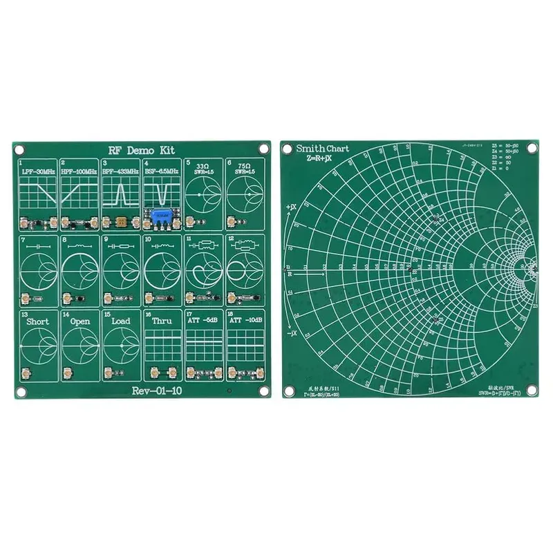
RF Board VNA Testing
Achieving robust performance in Massive MIMO RF boards is non-negotiable for the success of 5G and next-generation wireless systems. At Zero One Solution Limited, our unwavering commitment to quality assurance and rigorous testing protocols ensures that every RF board we deliver not only meets but exceeds the stringent demands of high-frequency applications. This meticulous approach guarantees unparalleled reliability, signal integrity, and long-term stability, critical for the complex, multi-antenna arrays at the heart of Massive MIMO.
How does Zero One Solution Limited ensure the signal integrity of Massive MIMO RF boards? We employ a multi-faceted approach to guarantee signal integrity. This includes precise impedance control through advanced design and manufacturing processes, utilizing specialized high-frequency substrate materials like Rogers and Teflon, and performing Time Domain Reflectometry (TDR) measurements during testing to verify characteristic impedance along transmission lines. Our designs also incorporate sophisticated grounding and shielding techniques to minimize crosstalk and external interference, crucial for maintaining signal purity in high-density RF environments.
Testing Methodology
Purpose
Key Benefit for Massive MIMO RF Boards
Vector Network Analyzer (VNA) Measurements
Characterizes RF performance (S-parameters, insertion loss, return loss) across a broad frequency range.
Ensures optimal signal transmission and reception efficiency for all antenna elements, critical for beamforming accuracy and overall system capacity.
Impedance Testing (TDR/VNA)
Verifies characteristic impedance of transmission lines and controlled impedance traces.
Prevents signal reflections and power loss, maintaining signal integrity across numerous RF paths and supporting high data rates without distortion.
Assesses board reliability and performance under extreme environmental conditions.
Guarantees long-term operational stability and durability in diverse deployment scenarios, from base stations to specialized applications, reducing field failures.
Our comprehensive quality control extends beyond standard checks, incorporating advanced methodologies tailored specifically for the complexities of Massive MIMO. By integrating these rigorous testing phases throughout the manufacturing process, from raw material inspection to final product validation, we ensure that each Massive MIMO RF board is optimized for peak performance and built to withstand the demanding operational environments of modern wireless infrastructure.
Why Choose Zero One Solution Limited for Your Massive MIMO RF Board Needs?
For telecommunications pioneers and research institutions pushing the boundaries of 5G and beyond, selecting the right partner for Massive MIMO RF board solutions is paramount. Zero One Solution Limited stands as a beacon of excellence, offering a unique blend of agility, expertise, and a globally integrated supply chain that directly addresses the critical needs of next-generation wireless infrastructure development. Our commitment extends beyond mere manufacturing; we are an innovation enabler, ensuring your groundbreaking designs translate into high-performance, market-ready products with unmatched speed and reliability.
Rapid Prototyping and Accelerated R&D Cycles Zero One Solution Limited specializes in rapid-response R&D prototype manufacturing for complex RF boards. Our streamlined processes and dedicated engineering teams enable significantly reduced lead times, allowing clients to iterate designs quickly, test concepts efficiently, and accelerate their product development timelines for Massive MIMO applications. This agility is critical in fast-paced markets, providing a distinct competitive edge for our partners.
End-to-End Integrated Solutions We offer a comprehensive one-stop service, from initial PCB design and material selection to precision manufacturing and advanced assembly. This integrated approach ensures seamless project execution, consistent quality control across all stages, and optimal performance of your Massive MIMO RF boards. Our expertise spans the entire lifecycle, minimizing communication overheads and potential issues that arise from fragmented supply chains.
Unwavering Quality and Rigorous Testing Protocols Quality is the cornerstone of our operations. For Massive MIMO RF boards, where performance at high frequencies is critical, we implement stringent quality assurance and testing methodologies. This includes advanced VNA (Vector Network Analyzer) measurements, precise impedance testing, and environmental stress testing, guaranteeing that every board meets the most demanding industry standards and client-specific requirements for robust RF performance in 5G and future networks.
Feature
Zero One Solution Limited's Advantage
Benefit for Massive MIMO RF Board Projects
Rapid Turnaround
Specialized rapid prototyping facilities and agile processes
Accelerates R&D, reduces time-to-market for innovative Massive MIMO solutions
Integrated Services
Full-spectrum PCB design, manufacturing, and assembly
Ensures seamless project flow, consistent quality, and optimized performance
RF Expertise
Dedicated engineering team with deep knowledge of high-frequency materials and design
Guarantees precision and reliability in complex Massive MIMO RF circuits
Global Reach
Strategic locations in Shenzhen (HQ) and Dubai (Branch)
Facilitates efficient logistics, supply chain access, and support for international clients
Delivers robust, high-performance Massive MIMO RF boards meeting stringent standards
The demands of Massive MIMO for 5G and future wireless technologies are pushing the boundaries of RF board design and manufacturing. At Zero One Solution Limited, our commitment to rapid prototyping, combined with our comprehensive one-stop services from design to assembly, positions us as the ideal partner for developing high-performance Massive MIMO RF board solutions. With our strategic global footprint, including operations in Shenzhen and Dubai, we ensure seamless access to resources and expertise, enabling our clients to accelerate their product development and maintain a competitive edge. Partner with us to transform your innovative concepts into market-ready realities and build the future of wireless communication. Contact Zero One Solution Limited today to discuss your next-generation RF board project.