In today's interconnected world, high-quality voice communication is paramount. Voice over LTE (VoLTE) technology has revolutionized mobile connectivity, offering superior call quality and seamless integration with data services. But what drives the reliability and performance of these cutting-edge devices? At its core lies the Printed Circuit Board (PCB). As a veteran engineer from Zero One Solution Limited, I can tell you that the complexity of VoLTE terminal PCBs demands unparalleled expertise in design, manufacturing, and assembly. This article delves into how Zero One Solution Limited, a leader in rapid-response R&D prototype manufacturing, provides comprehensive VoLTE Terminal PCB Solutions that empower our clients to bring innovative and high-performance products to market with exceptional efficiency.
The Critical Role of PCB in VoLTE Terminals
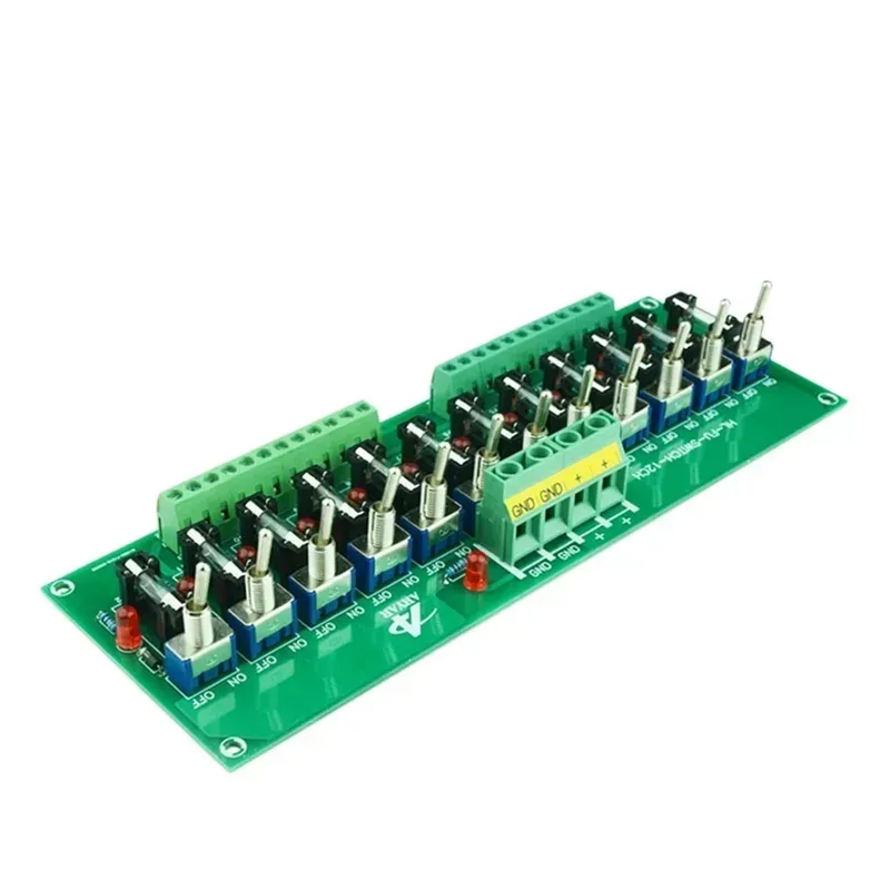
VoLTE Terminal PCB Board
At the core of every high-performing Voice over LTE (VoLTE) terminal lies a meticulously engineered Printed Circuit Board (PCB). Far from being a mere substrate, the PCB is the foundational backbone that dictates a VoLTE device's signal integrity, power management efficiency, and seamless component integration. Its design and manufacturing directly impact the device's ability to deliver crystal-clear voice calls, maintain robust data connections, and ensure reliable operation in complex RF environments, making it an indispensable element for the overall performance and reliability of VoLTE technology.
Aspect
Impact on VoLTE Performance
Zero One Solution's Approach
Signal Integrity
Critical for clear voice transmission and stable data; avoids distortion and dropped calls.
Precision routing, impedance control, and advanced material selection to minimize signal loss and interference at high frequencies.
Power Management Efficient power distribution is essential for extended battery life and stable operation, especially given the continuous data processing in VoLTE devices. Our designs prioritize optimal power delivery networks (PDN) and thermal dissipation strategies to ensure consistent power supply and prevent overheating, extending device longevity and performance.
Key VoLTE PCB Design Considerations
Challenge
Zero One Solution's Expertise
High-Frequency Routing
Managing signal loss and crosstalk at LTE frequencies (up to 2.6 GHz and beyond).
Utilizing specialized low-loss laminates, precise trace impedance matching, and advanced simulation tools to optimize signal paths.
Component Integration VoLTE terminals require the integration of numerous complex components, including RF transceivers, baseband processors, memory, and power management ICs, within a compact footprint. Our expertise in multi-layer PCB design and advanced packaging techniques enables high-density integration while maintaining optimal electrical performance and manufacturability.
Challenges in VoLTE Terminal PCB Design
Designing Printed Circuit Boards (PCBs) for Voice over LTE (VoLTE) terminals presents a complex array of challenges, primarily driven by the stringent demands of high-frequency communication, compact form factors, and robust power management. The intricate interplay of signal integrity, thermal dissipation, and electromagnetic compatibility (EMC) in a limited space dictates a meticulous design approach to ensure optimal performance, reliability, and compliance with telecommunication standards.
Design Challenge
Impact on VoLTE Terminal Performance
Key Design Considerations
High-Frequency Signal Routing
Degraded signal quality, data loss, increased power consumption
Minimizing trace length, maintaining consistent impedance, crosstalk prevention, use of specialized low-loss materials (e.g., Rogers, Isola)
Impedance Control
Signal reflections, standing waves, reduced transmission efficiency
Precise trace width/spacing, dielectric constant consistency, use of simulation tools (e.g., Ansys HFSS)
Why is high-frequency signal routing a major challenge in VoLTE PCB design? VoLTE operates at high frequencies, making signals highly susceptible to impedance mismatches, reflections, and electromagnetic interference. Even minor deviations in trace geometry or material properties can lead to significant signal degradation, impacting call quality and data throughput. Precise impedance control and careful routing are paramount to maintain signal integrity and ensure efficient data transmission across the PCB.
Zero One Solution's Expertise in VoLTE PCB Design
Zero One Solution Limited stands as a beacon of engineering excellence in the realm of VoLTE terminal PCB design. Our unparalleled expertise is rooted in a deep understanding of the intricate demands of high-frequency signal integrity, power efficiency, and compact form factor integration critical for reliable VoLTE device performance. We leverage a multidisciplinary team of seasoned engineers and state-of-the-art design tools to navigate complex challenges, ensuring every VoLTE PCB we design delivers optimal performance and unwavering reliability in the field.
Signal Integrity Mastery Our engineers possess profound expertise in managing high-frequency signals inherent in VoLTE. We meticulously design layouts to minimize impedance mismatches, crosstalk, and electromagnetic interference (EMI), crucial for crystal-clear voice and stable data transmission. This involves precise trace routing, differential pair management, and strategic component placement to maintain signal integrity across all layers.
Advanced Power Management Integration VoLTE terminals demand sophisticated power management to ensure extended battery life and consistent performance. Our design philosophy incorporates efficient power delivery networks (PDN), optimized voltage regulators, and thermal considerations directly into the PCB layout, preventing voltage drops and hot spots that could compromise device functionality or longevity.
Thermal Management Solutions The compact nature of VoLTE devices necessitates superior thermal management. We implement advanced thermal dissipation techniques within the PCB design, utilizing thermal vias, optimized copper pours, and strategic component placement to effectively manage heat generation, ensuring device stability and preventing performance degradation over time.
Stable power supply, extended battery life, and reduced noise interference
Component Placement
Strategic placement for thermal management, minimal trace length, and EMI reduction
Improved thermal performance, reduced signal degradation, and enhanced reliability
Material Selection
Utilizing low-loss tangent materials (e.g., Rogers, Isola) for RF sections
Minimizes signal attenuation and power loss, crucial for high-frequency VoLTE signals
Rapid Prototyping for VoLTE Device Development
Engineer Holding PCB Prototype
In the fast-evolving telecommunications landscape, rapid prototyping for VoLTE terminal PCB solutions is not merely an advantage but a critical imperative for market leadership. It significantly shortens the product development lifecycle, allowing innovators to validate designs, identify potential issues, and iterate quickly before committing to large-scale production. Zero One Solution Limited excels in this domain, providing an unparalleled rapid prototyping service that empowers clients to accelerate their R&D cycles and achieve faster time-to-market for their cutting-edge VoLTE devices.
Accelerated Design Validation Our rapid prototyping services enable quick validation of VoLTE PCB designs, ensuring that high-frequency signal integrity, power delivery, and component placement meet stringent performance requirements early in the development phase. This iterative approach minimizes costly redesigns and delays.
Optimized Iteration Cycles With fast turnaround times, clients can swiftly test multiple design iterations, comparing performance characteristics and refining functionalities. This agility is crucial for optimizing critical parameters like impedance control, thermal management, and EMI/EMC compliance specific to VoLTE applications.
Reduced Time-to-Market By compressing the prototyping phase, Zero One Solution directly contributes to a significantly reduced time-to-market for new VoLTE terminals. This allows our clients to gain a competitive edge by introducing innovative products to consumers ahead of the curve, capitalizing on emerging market demands.
Advanced Manufacturing Techniques for VoLTE PCBs
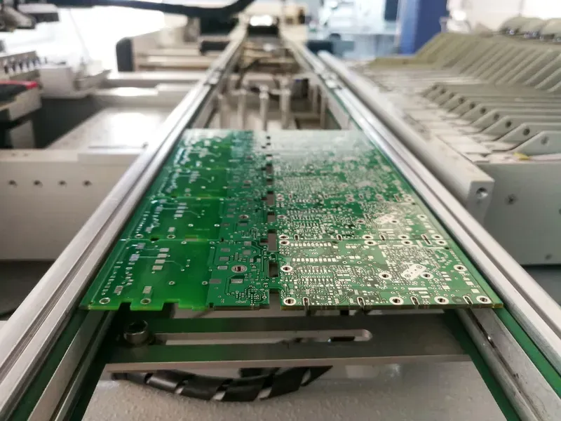
PCB Manufacturing Production Line
Advanced manufacturing techniques are paramount in realizing the high-performance and reliability demands of VoLTE (Voice over LTE) terminal PCBs. Zero One Solution Limited employs state-of-the-art processes that meticulously address the complexities of high-frequency signal transmission and compact device integration. Our approach ensures optimal material selection, precise layer stacking, and stringent quality control, culminating in PCBs that stand at the forefront of telecommunications technology.
Material Selection for High-Frequency Performance For VoLTE PCBs, the choice of substrate material is critical to minimize signal loss and maintain signal integrity at high frequencies. We utilize advanced low-loss dielectric materials, such as specific grades of FR-4 with enhanced performance, or specialized materials like high-Tg laminates and ceramic-filled PTFE composites, which offer superior dielectric constant stability and low dissipation factors essential for RF circuits. This ensures minimal attenuation and crosstalk for the intricate RF signal paths within VoLTE devices, directly impacting call quality and data throughput.
Precision Layer Stacking and Impedance Control VoLTE PCBs often feature multi-layer designs (e.g., 8-16 layers) to accommodate complex circuit densities and provide effective EMI shielding. Our manufacturing process employs highly precise layer stacking configurations optimized for controlled impedance routing. Through sophisticated impedance modeling and stack-up design tools, we accurately predict and control characteristic impedance (e.g., 50 Ohm for RF lines, 90/100 Ohm for differential pairs), which is vital for preventing signal reflections and ensuring efficient power transfer across the board. This precision prevents signal degradation and ensures robust data transmission.
Minimizes signal loss and distortion at VoLTE's high operating frequencies (e.g., 700MHz-2.6GHz bands).
Lamination
Vacuum Press Lamination
Ensures void-free lamination, preventing delamination and improving signal integrity, critical for compact VoLTE form factors and thermal dissipation.
Drilling
Laser Drilling for Microvias
Enables higher interconnect density, crucial for miniaturization and complex component integration in advanced VoLTE chipsets, facilitating HDI designs.
Surface Finish
ENIG (Electroless Nickel Immersion Gold) or OSP (Organic Solderability Preservative)
Provides excellent solderability and long-term reliability for fine-pitch components (e.g., BGA, QFN) prevalent in VoLTE ICs, enhancing connection stability and corrosion resistance.
Advanced Trace Routing and Spacing With the increasing complexity and component density in VoLTE terminals, our manufacturing capabilities extend to extremely fine trace widths and spaces (e.g., 3 mil/3 mil or less). This is achieved through advanced photolithography and etching techniques, allowing for intricate routing of high-speed digital and RF signals while maintaining critical isolation to prevent interference. Proper spacing also facilitates thermal management in densely packed areas, crucial for the sustained performance of VoLTE chipsets.
Rigorous Quality Control and Testing Every VoLTE PCB manufactured undergoes a multi-stage quality control process. This includes Automated Optical Inspection (AOI) for detecting manufacturing defects like opens, shorts, and solder mask issues, and Electrical Test (E-test) for continuity and isolation verification. For high-frequency designs, we also implement Time Domain Reflectometry (TDR) measurements to verify impedance control on critical signal lines. This comprehensive testing regimen ensures that each PCB meets stringent performance specifications and reliability standards, minimizing field failures and optimizing device performance.
Comprehensive VoLTE PCB Assembly Services
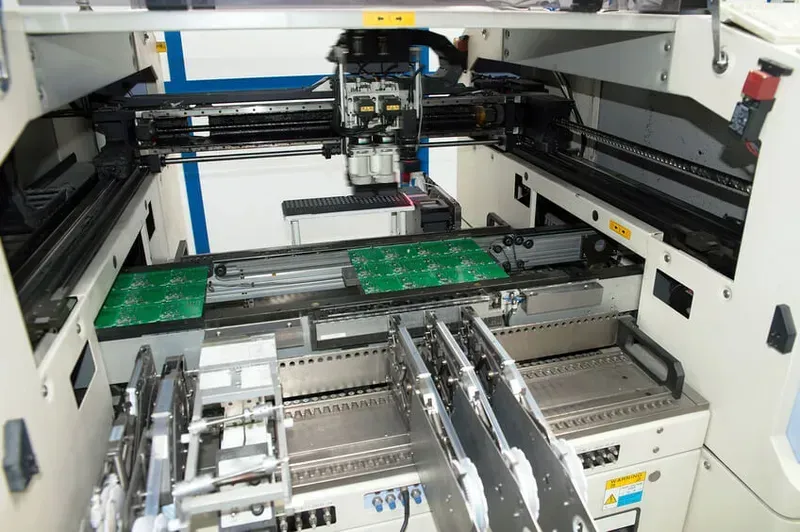
SMT Machine Assembling PCB
Achieving peak performance and unwavering reliability in VoLTE terminals necessitates a comprehensive and meticulously executed PCB assembly process. Zero One Solution Limited offers end-to-end VoLTE PCB assembly services, extending beyond mere component placement to encompass strategic component sourcing, advanced Surface Mount Technology (SMT), and rigorous post-assembly testing. This integrated approach ensures that every VoLTE PCB functions optimally, meeting the stringent demands of modern telecommunications and accelerating time-to-market for our clients.
Strategic Component Sourcing and Management Leveraging our extensive global supply chain network and strategic partnerships, we ensure the acquisition of high-quality, authentic components crucial for VoLTE performance. Our proactive component management mitigates supply chain risks and optimizes cost-efficiency, ensuring the long-term viability and reliability of your VoLTE devices.
Advanced Surface Mount Technology (SMT) Our state-of-the-art SMT lines are equipped with high-precision pick-and-place machines, automated optical inspection (AOI), and advanced reflow ovens. This enables us to handle fine-pitch components, BGA packages, and complex multi-layer designs common in VoLTE PCBs, ensuring accurate placement and robust soldering for optimal signal integrity.
Through-Hole Technology (THT) Integration For specific VoLTE terminal requirements, we seamlessly integrate Through-Hole Technology (THT) assembly, often for connectors or power components, ensuring robust mechanical and electrical connections. Our skilled technicians meticulously manage manual and automated THT processes to meet stringent quality standards.
Rigorous In-Circuit Testing (ICT) and Functional Testing (FCT) Post-assembly, every VoLTE PCB undergoes exhaustive In-Circuit Testing (ICT) to verify component presence, orientation, and electrical continuity. This is followed by Functional Testing (FCT), which simulates real-world operating conditions to validate the entire circuit's performance against design specifications, ensuring reliable voice and data transmission.
Conformal Coating and Potting For enhanced durability and environmental protection, particularly in demanding VoLTE applications, we offer conformal coating and potting services. These protective layers safeguard the PCB and its components from moisture, dust, chemical exposure, and mechanical shock, extending the operational lifespan of the terminal.
Comprehensive Quality Control and Traceability Our assembly process is underpinned by a robust Quality Management System (QMS), including IPC standards compliance (e.g., IPC-A-610 Class 2/3), real-time process monitoring, and complete traceability of all components and assembly steps. This ensures consistent quality, reduces defect rates, and provides full transparency for compliance and auditing purposes.
Ensuring Quality and Reliability: Testing and Validation
Engineer Testing PCB Board
In the demanding landscape of VoLTE terminal development, ensuring the quality and reliability of the Printed Circuit Board (PCB) is paramount. Rigorous testing and validation procedures are indispensable, as they guarantee optimal performance, signal integrity, and long-term durability in real-world operating conditions, ultimately preventing costly failures and accelerating market readiness.
Signal Integrity Testing Signal integrity testing is critical for high-speed VoLTE PCBs to prevent data loss and ensure clear communication. This involves time-domain reflectometry (TDR) to analyze impedance mismatches, eye diagrams to evaluate signal quality and jitter, and scattering parameter (S-parameter) analysis to characterize transmission line performance across the operating frequency range. Our advanced testing ensures minimal reflection and crosstalk, maintaining robust signal transmission essential for voice and data over LTE networks.
Functional Testing Functional testing validates that the VoLTE PCB operates as intended under various conditions. This includes power-on self-tests (POST), in-circuit testing (ICT) to check for manufacturing defects and component placement, and comprehensive functional test setups that simulate real-world usage scenarios. We verify component interaction, power consumption, and logical functions, ensuring the PCB meets all specified operational parameters for Voice over LTE applications.
Environmental Reliability Assessments Environmental reliability assessments subject VoLTE PCBs to extreme conditions to predict their performance and longevity in diverse environments. This includes thermal cycling to evaluate solder joint integrity and material expansion, humidity testing to assess moisture resistance, and vibration testing to simulate physical stress. These assessments confirm the PCB's resilience against environmental stressors, crucial for devices used globally in varied climates and conditions.
Why Choose Zero One Solution for Your VoLTE Terminal PCB Needs?
Choosing the right partner for your VoLTE terminal PCB solution is paramount for achieving market leadership and product excellence. Zero One Solution Limited stands as a beacon of innovation and reliability in this highly specialized domain, offering a unique blend of rapid-response capabilities, comprehensive end-to-end services, and a strategically integrated global supply chain network. Our unwavering commitment to client success and ability to navigate complex technical challenges ensures that your VoLTE devices are not only performant but also delivered to market with unparalleled speed and efficiency.
Rapid-Response R&D Prototyping We excel in rapid prototyping, drastically reducing time-to-market for your VoLTE devices. Our agile processes and advanced manufacturing facilities enable us to deliver high-quality prototypes with unmatched speed, allowing for swift iterations and accelerated product development cycles. This capability is critical for staying competitive in the fast-paced telecommunications industry.
Comprehensive One-Stop Services From initial PCB design and engineering to advanced manufacturing and final assembly, Zero One Solution provides a seamless, integrated service offering. This holistic approach eliminates the complexities of managing multiple vendors, ensuring consistent quality, streamlined communication, and a unified project execution from conception to mass production for your VoLTE terminal PCBs.
Global Supply Chain Network Advantage Leveraging our headquarters in Shenzhen and a branch in Dubai, we operate within a robust global PCBA supply chain network. This strategic positioning guarantees access to a diverse range of high-quality components and materials, enabling cost-effective solutions, mitigating supply chain risks, and ensuring timely delivery for your VoLTE PCB requirements, irrespective of scale or complexity.
FAQs about VoLTE Terminal PCB Solutions
Navigating the complexities of VoLTE terminal PCB solutions can raise numerous questions for developers and manufacturers. This section addresses common inquiries regarding the design, manufacturing, and assembly of VoLTE PCBs, offering clear, authoritative insights to help you make informed decisions and accelerate your product development.
What makes VoLTE PCB design uniquely challenging compared to standard mobile device PCBs? VoLTE (Voice over LTE) PCBs present unique challenges primarily due to the stringent requirements for high-frequency signal integrity, low latency, and robust power management. Unlike traditional voice communication, VoLTE transmits voice as data packets over an LTE network, demanding precise impedance control, minimized electromagnetic interference (EMI), and efficient thermal dissipation to maintain call quality and device performance. The integration of multiple high-speed RF components in a compact form factor further complicates routing and signal isolation, requiring advanced multi-layer stack-ups and specialized material selection to prevent signal degradation and cross-talk, which are critical for seamless voice transmission and reception.
How does Zero One Solution ensure signal integrity in high-frequency VoLTE PCB designs? Zero One Solution employs a multi-faceted approach to ensure superior signal integrity in high-frequency VoLTE PCB designs. This includes meticulous impedance matching for all high-speed traces, utilizing controlled impedance routing techniques, and optimizing layer stack-ups to minimize signal loss and reflection. We leverage advanced simulation tools to predict and mitigate signal integrity issues before manufacturing. Additionally, careful consideration is given to power delivery network (PDN) design to ensure stable voltage rails, and strategic component placement combined with effective grounding schemes helps reduce noise and EMI, safeguarding the clarity and reliability of VoLTE communications.
What materials are critical for optimal VoLTE PCB performance, and why? For optimal VoLTE PCB performance, critical materials include low-loss dielectric substrates such as Rogers materials or high-performance FR-4 variants with low Dk (dielectric constant) and Df (dissipation factor). These materials are crucial for minimizing signal attenuation and distortion at the high frequencies (typically 700MHz to 2.6GHz for LTE bands) used in VoLTE. High-quality copper foils are also essential for excellent conductivity and thermal dissipation. The choice of solder mask and surface finishes like ENIG (Electroless Nickel Immersion Gold) ensures reliable soldering, corrosion resistance, and stable electrical contact, all contributing to the longevity and consistent performance of the VoLTE terminal.
Can Zero One Solution support rapid prototyping for complex VoLTE PCB designs? Absolutely. Zero One Solution specializes in rapid prototyping services tailored for complex designs, including VoLTE PCBs. Our streamlined internal processes, dedicated high-speed manufacturing lines, and extensive component sourcing network allow for significantly reduced lead times from design finalization to prototype delivery. This rapid turnaround empowers our clients to iterate on their VoLTE device designs quickly, test functionalities, and validate performance, thereby accelerating their R&D cycles and significantly shortening time-to-market for innovative VoLTE-enabled products. Our Shenzhen and Dubai offices further optimize global supply chain access and support for expedited project timelines.
The intricacies of VoLTE terminal development necessitate a PCB solution provider that understands the critical balance between performance, reliability, and speed. Zero One Solution Limited, with its deep expertise and strategic global presence, is uniquely positioned to be your trusted partner. We offer end-to-end VoLTE Terminal PCB Solutions, from initial design consultation to rapid prototyping, manufacturing, and assembly, ensuring your innovations not only meet but exceed market demands. Don't let PCB complexities slow down your next big product. Partner with Zero One Solution Limited and accelerate your journey from concept to market leader. Visit our website or contact us today to discuss how our VoLTE Terminal PCB Solutions can empower your next breakthrough.