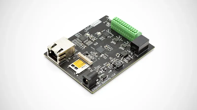
In today's interconnected world, voice gateways play a crucial role in bridging traditional telephone networks with modern IP-based communication systems. At the heart of these gateways lies the Printed Circuit Board (PCB), a critical component that dictates performance, reliability, and scalability. Zero One Solution Limited, with its extensive experience in rapid PCB prototyping and one-stop services, offers comprehensive voice gateway PCB solutions designed to meet the evolving demands of the telecommunications industry. Are you seeking a reliable partner to accelerate your voice gateway development? Look no further. This article delves into the intricacies of voice gateway PCB solutions, highlighting design considerations, manufacturing processes, and the benefits of partnering with a trusted provider like Zero One Solution.
Understanding Voice Gateways and Their Importance
Voice gateways are pivotal components in modern communication infrastructures, serving as the crucial bridge between traditional Public Switched Telephone Networks (PSTN) and Voice over Internet Protocol (VoIP) systems. This vital interconnection facilitates seamless voice communication, enabling enterprises and service providers to leverage the cost-effectiveness and flexibility of IP-based telephony while retaining connectivity with legacy systems. Their fundamental role ensures interoperability, allowing diverse communication platforms to coexist and function as a unified network.
Bridging Legacy and Modern Networks Voice gateways act as translators, converting analog voice signals from traditional phone lines into digital packets for IP networks, and vice-versa. This enables calls to traverse between PSTN and VoIP seamlessly, ensuring continuity in communication services during transitions to modern infrastructure or hybrid deployments.
Enabling Cost-Effective VoIP Deployments By facilitating the integration of existing analog devices like fax machines, modems, and traditional telephones with VoIP systems, voice gateways reduce the need for complete hardware overhauls. This approach significantly lowers initial investment and operational costs for businesses adopting VoIP technology.
The demand for robust and reliable voice gateway solutions is escalating across various industries due to the pervasive shift towards converged communication platforms and remote work models. From enterprise communication systems to call centers and service provider networks, voice gateways underpin the efficiency and resilience of contemporary voice services. Their ability to manage diverse call routing, ensure quality of service (QoS), and support various signaling protocols makes them indispensable for businesses aiming to optimize their communication infrastructure.
Application Area
Importance of Voice Gateway
Key Benefit
Enterprise Telephony
Connects existing PBX systems to VoIP networks, enabling unified communications.
Cost savings, enhanced features (e.g., video conferencing)
Call Centers
Manages high volumes of inbound/outbound calls, integrates with CRM.
Improved customer service, operational efficiency
Service Providers
Offers diverse connectivity options for subscribers, manages network traffic.
Scalability, reliable service delivery
Remote Office Connectivity
Links remote users to the main corporate network via VoIP.
Flexible work arrangements, reduced communication costs
Key Design Considerations for Voice Gateway PCBs
Voice Gateway PCB Design
Designing high-performance Voice Gateway PCBs requires meticulous attention to several critical factors that directly impact their reliability, functionality, and compliance. From ensuring pristine signal transmission to efficient power distribution and thermal dissipation, each design decision is pivotal in creating a robust and long-lasting solution capable of handling the demands of modern communication networks. Adherence to industry standards and regulatory requirements is not merely a formality but a foundational element that ensures interoperability, safety, and market acceptance.
Signal Integrity (SI) Maintaining signal integrity is paramount for high-speed digital and analog signals within voice gateways. This involves careful impedance matching, minimizing crosstalk, and reducing electromagnetic interference (EMI). Techniques such as controlled impedance traces, proper ground plane design, and differential pair routing are crucial to prevent signal degradation and ensure clear voice transmission. Simulation tools are often employed to predict and optimize SI performance during the design phase, mitigating potential issues before manufacturing.
Power Management Efficient power management is vital for the stable operation and longevity of Voice Gateway PCBs. This includes designing robust power delivery networks (PDN) to minimize voltage drops and ripple, selecting appropriate voltage regulators (LDOs, buck/boost converters), and ensuring proper decoupling capacitance. Effective power management not only enhances performance but also contributes to reduced power consumption and heat generation, which are critical for reliability and operating costs.
Thermal Considerations Voice gateways, especially those handling high traffic, can generate significant heat. Effective thermal management is essential to prevent component overheating, which can lead to reduced performance, instability, and premature failure. Design strategies include optimizing component placement for airflow, utilizing thermal vias, incorporating heat sinks, and considering the overall enclosure design. Thermal simulation helps predict temperature distributions and ensures the PCB operates within safe temperature limits.
Component Selection The choice of components directly influences the performance, reliability, and cost of the Voice Gateway PCB. This involves selecting high-quality processors, codecs, memory, and communication interfaces that meet the required specifications for voice processing, network connectivity, and power efficiency. Factors such as operating temperature range, lifespan, availability, and cost-effectiveness must be carefully balanced to achieve an optimal design without compromising on quality or performance.
Regulatory Compliance and Standards Adhering to industry standards (e.g., IEEE, ITU-T) and regulatory requirements (e.g., FCC, CE, RoHS) is non-negotiable for Voice Gateway PCBs. These standards ensure interoperability, safety, electromagnetic compatibility (EMC), and environmental responsibility. Designs must incorporate features to meet these requirements, such as proper EMI shielding, surge protection, and material compliance, to facilitate smooth certification processes and market entry.
Material Selection for Optimal Performance and Reliability in Voice Gateway PCBs
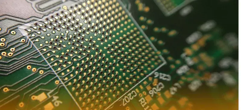
PCB Material Close-Up
The selection of appropriate materials is paramount in the fabrication of Voice Gateway PCBs, directly influencing their electrical performance, thermal stability, and long-term reliability. Sub-optimal material choices can lead to issues such as signal degradation, increased power consumption, and reduced operational lifespan. Therefore, a meticulous approach to material specification, considering dielectric properties, thermal conductivity, and mechanical strength, is essential for ensuring robust and high-performing voice gateway solutions.
Material Type
Key Properties
Impact on Voice Gateway PCB Performance
FR-4
Standard glass-reinforced epoxy laminate; good balance of electrical and mechanical properties.
Cost-effective, suitable for many voice gateway applications, but can have higher signal loss at very high frequencies.
Essential for designs with higher component density or operating temperatures, preventing delamination and ensuring stability.
Low-Loss Laminates (e.g., Rogers, Isola)
Lower dielectric constant (Dk) and dissipation factor (Df); excellent signal integrity at higher frequencies.
Minimizes signal loss and crosstalk, crucial for high-speed data transmission within voice gateways, leading to clearer voice quality.
Copper Foils
Conductive layer; varying thickness (e.g., 0.5 oz to 2 oz).
Thicker copper (2 oz) enhances current carrying capacity and thermal dissipation, vital for power planes and minimizing IR drop in complex voice gateway designs.
Solder Mask
Protective polymer layer; insulates circuits and prevents solder bridging.
High-quality solder mask ensures long-term protection against environmental factors and prevents short circuits, contributing to device longevity.
Surface Finishes (e.g., ENIG, HASL)
Protects exposed copper, ensures solderability.
ENIG (Electroless Nickel Immersion Gold) offers superior flatness for fine-pitch components and excellent shelf life, critical for high-density voice gateway boards.
Manufacturing Processes: Ensuring Precision and Quality
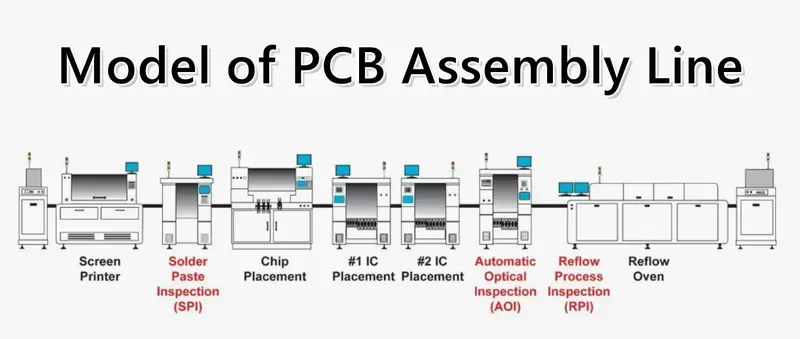
PCB Production Line
The precision and quality of a Voice Gateway PCB are paramount for reliable communication, making the manufacturing process a critical stage. From initial fabrication to final surface finishing, each step demands meticulous attention to detail and adherence to stringent quality controls to ensure the robust performance and longevity of these essential components. A flawed manufacturing process can introduce signal integrity issues, power distribution problems, and ultimately, system failures, directly impacting the voice clarity and connectivity that voice gateways are designed to facilitate.
PCB Fabrication This initial stage involves preparing the raw laminate material. High-quality laminates, often chosen for their dielectric properties and thermal stability, are cut to size. The quality of this foundational step directly influences the subsequent layers' adhesion and overall structural integrity.
Drilling Precise drilling creates the necessary holes for through-hole components, vias (interconnects between layers), and mounting points. For Voice Gateway PCBs, accuracy is critical, particularly for high-density interconnect (HDI) designs that utilize microvias, ensuring reliable electrical connections and signal paths.
Plating Electroless and electrolytic plating processes deposit a conductive layer, typically copper, into the drilled holes and onto the surface to form conductive traces. This step is vital for establishing robust electrical connections between layers and for preparing the surface for subsequent etching.
Etching During etching, unwanted copper is chemically removed, leaving behind the designed circuit traces and pads. Controlled etching is essential to maintain trace impedance and width tolerances, which are critical for high-frequency signal transmission in voice gateway applications.
Soldermask Application A protective soldermask layer is applied over the traces, leaving only the solder pads exposed. This prevents solder bridges during assembly, protects the copper traces from oxidation, and provides electrical insulation, enhancing the PCB's durability and reliability in diverse operating environments.
Surface Finishing The exposed copper pads receive a surface finish, such as ENIG (Electroless Nickel Immersion Gold) or OSP (Organic Solderability Preservative), to protect them from oxidation and ensure excellent solderability during component assembly. For Voice Gateway PCBs, an optimal surface finish ensures strong, reliable solder joints for critical components.
Quality Control and Testing Throughout the entire manufacturing cycle, rigorous quality control measures are implemented. This includes Automated Optical Inspection (AOI) for defect detection, Electrical Test (E-Test) for open/short circuits, and X-ray inspection for complex multi-layer boards. These comprehensive tests guarantee that each Voice Gateway PCB meets stringent performance and reliability standards before leaving the factory. For instance, E-tests can identify minute discontinuities in signal paths that might otherwise lead to intermittent voice connectivity issues.
Advanced PCB Technologies for Enhanced Functionality
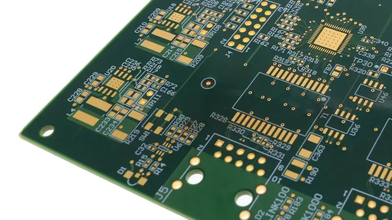
Multi-layer PCB Board Close-Up
To achieve optimal performance, miniaturization, and signal integrity in Voice Gateway PCB Solutions, integrating advanced PCB technologies is paramount. These innovations address the intricate demands of high-speed digital and analog signals, ensuring reliable and efficient data transmission crucial for modern communication infrastructure. Leveraging technologies such as multi-layer designs, blind and buried vias, and precise impedance control transforms a standard PCB into a high-performance platform capable of handling complex voice gateway operations with superior signal fidelity and reduced electromagnetic interference (EMI).
Multi-Layer PCBs for High-Density Integration Multi-layer PCBs are fundamental for Voice Gateway Solutions, allowing for significantly higher component density and more complex routing. By stacking multiple layers of conductive traces separated by insulating material, these boards enable shorter signal paths, improved power distribution, and effective shielding, all of which contribute to reduced noise and enhanced signal integrity. This is vital for voice gateways that process numerous simultaneous communication channels, demanding compact yet robust designs capable of handling high data throughput without degradation.
Blind and Buried Vias for Space Optimization Blind vias connect an outer layer to one or more inner layers, while buried vias connect two or more inner layers without extending to the surface. Both technologies are critical for maximizing routing space on densely populated Voice Gateway PCBs. By freeing up surface real estate and inner layers, they facilitate more intricate routing patterns, minimize layer count, and reduce parasitic capacitance, leading to improved electrical performance and smaller form factors. This is particularly beneficial for compact voice gateway devices where space is at a premium but performance cannot be compromised.
Impedance Control for Signal Integrity Impedance control is essential in Voice Gateway PCB design to ensure that high-frequency signals propagate without reflections or distortions, which could lead to data errors or signal loss. By carefully managing the dielectric constant of the materials, trace width, and spacing, designers can maintain a consistent characteristic impedance across critical signal lines. This precision is vital for maintaining the integrity of digital and analog voice signals, preventing crosstalk, and ensuring reliable communication in high-speed Voice Gateway applications. Accurate impedance matching ensures that signals are transmitted efficiently, preserving audio quality and connection stability.
Advanced PCB Technology
Benefit for Voice Gateway PCB
Impact on Performance
Multi-Layer PCBs
Increased component density, shorter signal paths, better EMI shielding
Enhanced signal integrity, reduced noise, higher data throughput
Miniaturization, lower parasitic capacitance, superior signal routing
Impedance Control
Consistent signal propagation, reduced reflections and distortions
Improved signal fidelity, prevention of data errors, stable communication
Zero One Solution's Voice Gateway PCB Capabilities
Electronics Engineer Operating Equipment
Zero One Solution Limited stands as a premier partner for comprehensive Voice Gateway PCB solutions, offering an end-to-end service from initial design and rapid prototyping to high-volume manufacturing and precise assembly. Leveraging our strategic location in Shenzhen, China, and our Dubai branch, we integrate seamlessly into the global PCBA supply chain, ensuring unparalleled efficiency and access to essential resources. Our capabilities are specifically tailored to meet the rigorous demands of voice gateway applications, delivering robust, high-performance PCBs that underpin reliable communication networks.
Rapid Prototyping Excellence At Zero One Solution, our core strength lies in rapid-response R&D prototype manufacturing. We accelerate your product development cycle for Voice Gateway PCBs by delivering high-fidelity prototypes swiftly, enabling quick iterations and validation of your designs. Our agile approach significantly reduces time-to-market for innovative voice communication products.
Comprehensive Design and Engineering Support Our team of veteran engineers provides extensive design support, optimizing your Voice Gateway PCB layouts for signal integrity, power efficiency, thermal management, and manufacturability. We ensure designs adhere to stringent industry standards and regulatory requirements, laying the groundwork for superior performance.
Advanced Manufacturing Precision We employ state-of-the-art manufacturing processes and cutting-edge equipment to produce Voice Gateway PCBs with exceptional precision and quality. This includes multi-layer fabrication, advanced drilling techniques, impedance control, and various surface finishes, all contributing to the reliability and longevity of the final product. Our commitment to quality control at every stage ensures consistency and eliminates potential defects.
High-Quality Component Sourcing and Management Leveraging our vast global network, we provide efficient and reliable sourcing of high-quality components critical for Voice Gateway PCBs. Our robust supply chain management mitigates risks, ensures authenticity, and optimizes procurement costs, translating into a more competitive final product without compromising on performance.
Precision PCBA and Testing Beyond manufacturing, Zero One Solution offers advanced PCB assembly (PCBA) services, utilizing automated SMT and PTH lines for precise component placement. Every Voice Gateway PCBA undergoes rigorous testing, including ICT (In-Circuit Test), functional testing, and environmental testing, to guarantee flawless operation and compliance with performance specifications.
One-Stop Service for Seamless Execution Our integrated 'one-stop' service model simplifies the entire Voice Gateway PCB development and production process. From conceptualization to final assembly and delivery, clients benefit from a single point of contact, streamlined communication, and a unified approach, eliminating complexities and accelerating project completion. This comprehensive solution saves valuable time and resources, allowing you to focus on innovation.
The Benefits of Partnering with Zero One Solution
Partnering with Zero One Solution Limited for your Voice Gateway PCB needs transcends a mere vendor relationship; it's a strategic alliance that propels your product development forward with unparalleled efficiency and assurance. Our comprehensive one-stop service, from design to assembly, is meticulously crafted to address the critical pain points in product realization, offering a clear competitive advantage in the rapidly evolving telecommunications landscape.
Accelerated Time-to-Market In the fast-paced electronics market, speed is paramount. Zero One Solution's rapid prototyping capabilities, honed over years of focused expertise, significantly reduce your development cycles. By streamlining design, manufacturing, and assembly processes under one roof, we eliminate coordination delays and accelerate your product's journey from concept to market readiness, ensuring you capitalize on emerging opportunities ahead of the competition. Our average prototype delivery time is 5-7 business days for standard PCBs, a testament to our optimized workflow and advanced machinery.
Reduced Development Costs & Optimized ROI Our integrated approach minimizes unforeseen costs often associated with fragmented supply chains. By offering a complete suite of services, we optimize material procurement, reduce logistical complexities, and provide economies of scale. This holistic management translates directly into lower overall development costs and a higher return on investment (ROI) for your Voice Gateway PCB projects. We work diligently to identify cost-effective solutions without compromising quality or performance, providing detailed cost breakdowns and material recommendations early in the process to ensure budgetary alignment.
Access to Unrivaled Engineering Expertise With a team of veteran engineers boasting decades of experience in PCB design, manufacturing, and assembly, Zero One Solution brings a wealth of knowledge to your project. Our experts are adept at navigating complex design challenges, ensuring signal integrity, power efficiency, and thermal management for high-performance Voice Gateway PCBs. This deep technical expertise guarantees that your product benefits from cutting-edge solutions and robust engineering practices from the outset. Our engineers are certified in IPC standards and are continuously updated on the latest industry innovations and best practices.
Unwavering Commitment to Quality and Reliability Quality is the cornerstone of our operations. Zero One Solution adheres to stringent quality control protocols at every stage, from material selection to final assembly and testing. Our state-of-the-art facilities and rigorous inspection processes ensure that every Voice Gateway PCB meets the highest standards of reliability and performance, minimizing post-production issues and enhancing product longevity. We maintain ISO 9001:2015 certification and implement automated optical inspection (AOI) and X-ray inspection for critical components, achieving a defect rate of less than 0.01% in our outgoing quality control.
Strategic Global Supply Chain Advantage Strategically located in Shenzhen, China's electronic manufacturing hub, and with a branch office in Dubai, Zero One Solution leverages a robust global PCBA supply chain network. This strategic positioning provides seamless access to a diverse range of high-quality components and raw materials, ensuring competitive pricing and consistent material availability, even for specialized Voice Gateway PCB components. Our dual-location strategy enhances logistical efficiency and risk mitigation, ensuring uninterrupted production and timely delivery, regardless of geopolitical or supply chain fluctuations.
Frequently Asked Questions (FAQs) About Voice Gateway PCBs
Navigating the complexities of Voice Gateway PCB solutions can raise numerous questions, from initial design considerations to final manufacturing and testing. This FAQ section aims to address the most common inquiries, providing clear, authoritative insights to help you better understand the critical aspects of Voice Gateway PCB development and deployment.
What is the primary function of a Voice Gateway PCB? The primary function of a Voice Gateway PCB is to facilitate the conversion and transmission of voice signals between different communication networks, typically bridging traditional analog or digital telephony systems (PSTN) with modern Voice over IP (VoIP) networks. It acts as a crucial interface, enabling seamless voice communication across disparate protocols and infrastructures.
Why is signal integrity critical in Voice Gateway PCB design? Signal integrity is paramount in Voice Gateway PCB design to ensure crystal-clear voice transmission without distortion, noise, or data loss. Poor signal integrity can lead to dropped calls, echo, or degraded audio quality. Critical factors include impedance matching, minimizing crosstalk, proper grounding, and managing signal reflections, especially for high-frequency digital audio signals.
What are the common challenges in manufacturing Voice Gateway PCBs? Manufacturing Voice Gateway PCBs presents challenges such as achieving precise impedance control for high-speed signals, managing thermal dissipation for complex chipsets, and ensuring high reliability for continuous operation. The integration of sensitive analog and digital components on a single board also requires meticulous attention to layout and assembly processes to prevent interference and ensure optimal performance.
How does Zero One Solution ensure the quality and reliability of Voice Gateway PCBs? Zero One Solution ensures the quality and reliability of Voice Gateway PCBs through a multi-faceted approach. This includes rigorous DFM (Design for Manufacturability) analysis, utilization of high-grade materials, advanced manufacturing processes with stringent quality control at every stage (e.g., AOI, X-ray inspection), and comprehensive functional testing before delivery. Our expertise in rapid prototyping also allows for iterative improvements and verification.
What advanced PCB technologies are beneficial for Voice Gateway applications? Advanced PCB technologies highly beneficial for Voice Gateway applications include multi-layer PCBs for enhanced signal routing and noise reduction, blind and buried vias for increased routing density and reduced board size, and controlled impedance traces to maintain signal integrity for high-frequency data. These technologies contribute to improved performance, reduced electromagnetic interference (EMI), and greater reliability.
Voice gateway PCBs are vital to modern communication systems, and their design and manufacturing require meticulous attention to detail. Zero One Solution Limited offers comprehensive solutions, from rapid prototyping to full-scale production, ensuring your voice gateway products meet the highest standards of performance and reliability. By partnering with Zero One Solution, you gain access to cutting-edge technologies, experienced engineers, and a global supply chain network, empowering you to accelerate product development and gain a competitive edge. Contact us today to discover how we can help you bring your innovative voice communication solutions to market faster and more efficiently. Let Zero One Solution be your trusted partner in voice gateway PCB solutions, enabling seamless communication across the globe.