
The demand for hyper-fast, low-latency connectivity is no longer a luxury—it is the baseline for modern digital infrastructure. As we transition from the standard-setting WiFi 6 to the transformative capabilities of WiFi 7, the pressure on the physical layer is reaching a breaking point. It is not just about firmware upgrades; it is about the very veins of the network: the printed circuit board (PCB) infrastructure.
The Architectural Shift: From WiFi 6 to WiFi 7

Redefining the Signal Path
The jump from WiFi 6 to WiFi 7 is not merely a software update; it is an infrastructure overhaul driven by the demand for massive throughput. WiFi 7 introduces 320MHz channel bandwidth, doubling the capacity of WiFi 6E and necessitating significant improvements in signal integrity at the physical layer. As frequencies push higher into the 6GHz spectrum, the PCB becomes a critical bottleneck, requiring advanced dielectric materials and tighter trace impedance control to mitigate insertion loss and electromagnetic interference.
Comparative Requirements for PCB Infrastructure
| Feature | WiFi 6 Requirement | WiFi 7 Requirement |
|---|---|---|
| Max Bandwidth | 160 MHz | 320 MHz |
| Material Loss (Df) | Standard FR-4 / Mid-loss | Ultra-low loss laminates |
| Impedance Tolerance | ±10% | ±5% or better |
| Thermal Management | Passive cooling | Enhanced copper weight/heat sinking |
Technical Challenges in WiFi 7 Implementation
- Why do 320MHz channels complicate PCB design?
Wider channels increase the noise floor and require a cleaner signal path to maintain high MCS rates, meaning even minor reflections or discontinuities on the PCB can cause significant data corruption. - How does insertion loss impact range?
At WiFi 7's higher frequencies, signal energy dissipates quickly within the board's dielectric layers; using high-performance, low-loss materials is essential to preserving link budget. - What role does thermal management play?
WiFi 7 chipsets operate at higher power densities to manage complex multi-link operations, requiring specialized PCB stackups to distribute heat effectively and prevent thermal throttling.
Signal Integrity Challenges at Multi-Gigabit Speeds
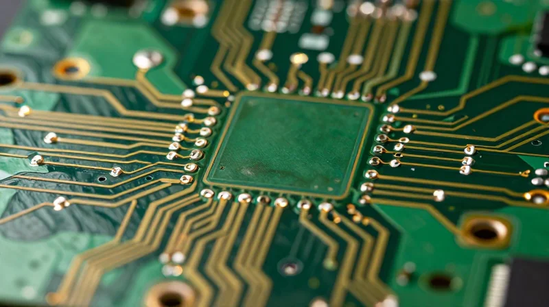
The Physics of High-Frequency Signal Degradation
As operating frequencies climb to support the 6GHz spectrum and 320MHz channel bandwidths, traditional PCB routing practices encounter severe physical limitations. The primary challenge stems from dielectric loss and conductor losses—skin effect and surface roughness—which accelerate exponentially as frequency increases. Unlike WiFi 6, where standard FR-4 materials might suffice for shorter traces, WiFi 7 necessitates substrates with ultra-low dissipation factors (Df) to minimize signal attenuation before it reaches the antenna.
Key Impedance and Crosstalk Factors
| Parameter | WiFi 6 Requirement | WiFi 7 Challenge |
|---|---|---|
| Return Loss | Acceptable at -10dB | Requires -15dB or better |
| Insertion Loss | Moderate tolerance | Critical; < 0.5dB/cm at 7GHz |
| Via Design | Standard through-hole | Blind/buried with back-drilling |
Mitigating High-Speed Routing Issues
Routing paths in WiFi 7 designs are no longer just connections; they are transmission lines that must be tuned to mitigate reflections caused by discontinuities. Improper impedance matching at connector pads or via transitions acts as a low-pass filter, effectively capping the effective bandwidth and inducing signal jitter. Engineers must now implement rigorous electromagnetic (EM) field simulation early in the design cycle to account for glass weave effects—a phenomenon where the non-homogeneous nature of fiberglass cloth creates local variations in dielectric constant, causing skew in differential pairs.
Frequently Asked Questions on Signal Integrity
- Why does copper surface roughness impact WiFi 7?
At multi-gigabit frequencies, current density shifts toward the surface of the copper trace. Rough copper surfaces increase the path length for electrons, thereby increasing resistive loss. - Is standard FR-4 viable for WiFi 7?
Generally, no. Standard FR-4 has a high dissipation factor that leads to excessive signal loss at 6GHz+, requiring a transition to high-frequency laminates like PTFE or advanced ceramic-filled resins. - How does back-drilling help signal integrity?
Back-drilling removes the unused portion of a via barrel (the stub). At high frequencies, these stubs act as capacitive antennas, creating resonance and reflections that degrade signal quality.
Advanced MIMO and Antenna Integration

Navigating High-Order MIMO Complexity
The transition to WiFi 7 features a massive leap in spatial streams, increasing from 8x8 MU-MIMO in WiFi 6 to 16x16 in advanced WiFi 7 implementations. This doubling of antenna elements on the PCB surface presents significant challenges for layout engineers, specifically regarding electromagnetic interference (EMI) and cross-talk. To support these streams, designers must implement high-density interconnect (HDI) technologies that allow for precise routing paths, minimizing the trace lengths that contribute to signal attenuation.
Spatial Optimization and Decoupling
With the increased density of antennas, maintaining adequate isolation between channels is critical to preventing desensitization of the receiver. PCB designers are now moving toward multi-layered substrate architectures that utilize buried vias and blind vias to isolate sensitive RF traces from high-speed digital switching noise. Furthermore, antenna placement must be optimized to ensure that near-field coupling does not degrade the beamforming capabilities inherent to WiFi 7.
| Feature | WiFi 6 Requirement | WiFi 7 Requirement |
|---|---|---|
| Max Spatial Streams | 8x8 | 16x16 |
| Routing Complexity | Moderate | Extreme |
| EMI Mitigation | Standard Shielding | Advanced Spatial Filtering |
| Board Density | Standard HDI | Advanced Any-Layer HDI |
Frequently Asked Questions
- How does 16x16 MIMO impact PCB footprint?
The increased number of antennas requires a larger keep-out zone and more complex routing, often necessitating a larger board surface area or the adoption of multi-layer PCB stacks to manage trace congestion. - Why is shielding more difficult in WiFi 7?
At the wider bandwidths and higher frequencies of WiFi 7, electromagnetic waves are more prone to coupling; this requires more localized shielding and better ground plane management to avoid signal degradation.
Material Science: Choosing the Right PCB Substrates
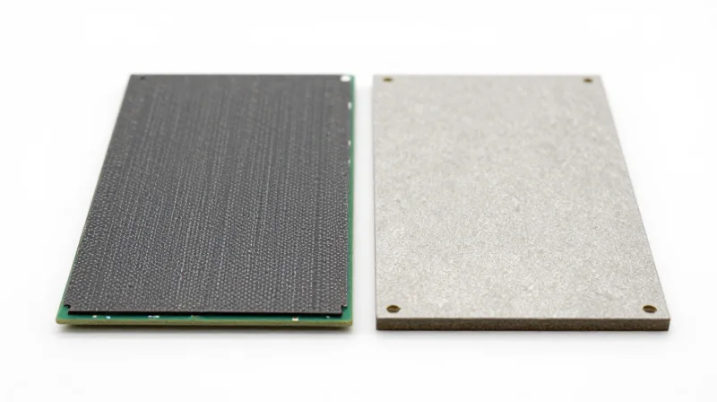
Material Science: Choosing the Right PCB Substrates
As WiFi 7 pushes operating frequencies higher and increases data throughput to support 320MHz channels, the substrate requirements undergo a fundamental shift. Standard FR-4 laminates, which perform adequately for WiFi 6, often exhibit excessive dielectric loss and thermal instability under the demanding power requirements of WiFi 7 chipsets. Engineers must transition to low-loss materials—typically high-frequency laminates or modified epoxy resins—to minimize signal attenuation and maintain the necessary thermal profile for long-term reliability.
Material Performance Comparison
| Material Class | Dielectric Loss (Df) | Thermal Conductivity | WiFi 7 Suitability |
|---|---|---|---|
| Standard FR-4 | High (>0.020) | Low | Poor |
| High-Tg FR-4 | Medium (0.015) | Moderate | Marginal |
| Low-Loss Laminate | Low (<0.005) | High | Excellent |
Critical Selection Factors
- Why is Dielectric Loss (Df) a primary concern for WiFi 7?
As signal frequency increases, the energy absorbed by the board material increases significantly. Low-loss materials are required to prevent signal attenuation and ensure packet integrity over the physical traces. - What role does Glass Transition Temperature (Tg) play?
WiFi 7 hardware generates significant heat due to complex modulation (4K-QAM) and MIMO processing. High-Tg materials prevent the substrate from softening or warping, which could cause dielectric breakdown or trace fatigue. - How does surface roughness impact performance?
Skin effect at high frequencies forces current to travel along the surface of copper traces. Using low-profile (smooth) copper foil is essential to reduce resistive losses that are exacerbated at the 6GHz bands utilized by WiFi 7.
Thermal Management in High-Density Router Designs
Addressing Thermal Flux in WiFi 7 Architectures
WiFi 7 chipsets operate with higher throughput and complex modulation schemes that result in localized hotspots exceeding the thermal profiles of WiFi 6. Effective heat management necessitates a transition from passive cooling to integrated board-level solutions, including enlarged copper pours, thermal vias arrays, and low-thermal-resistance interface materials that facilitate heat transfer to the enclosure chassis.
Comparative Thermal Strategies
| Feature | WiFi 6 Design Approach | WiFi 7 Design Approach |
|---|---|---|
| Copper Pour Strategy | Standard ground plane stitching | Thickened internal layers (2oz+) |
| Thermal Vias | Localized placement | High-density thermal via matrices |
| TIM Application | Standard interface pads | Phase-change materials or high-k gap fillers |
| Enclosure Integration | Airflow convection focus | Chassis-integrated heat sinking |
Frequently Asked Questions on Thermal Design
- How do higher frequencies affect thermal design?
Higher frequencies require thinner substrates to maintain signal integrity, which inherently reduces the thermal mass of the PCB; this necessitates compensating with advanced heat spreading techniques like metallic structural reinforcements. - Is active cooling mandatory for WiFi 7 routers?
While not always mandatory, active cooling is increasingly preferred for high-density enterprise routers to prevent the thermal throttling of MLO (Multi-Link Operation) features during peak utilization. - What is the role of High-Tg laminates in thermal management?
High-Tg materials prevent dielectric softening and structural delamination when boards are subjected to the prolonged elevated temperatures characteristic of power-hungry WiFi 7 chipsets.
The Role of Shielding and Noise Reduction
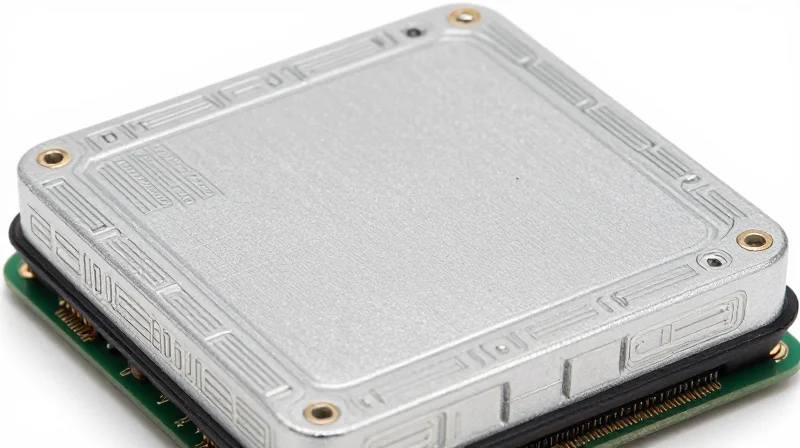
The Necessity of Advanced Shielding in WiFi 7
As WiFi 7 pushes frequency ranges into the 6GHz spectrum and demands wider 320MHz channels, the board-level environment becomes highly susceptible to Electromagnetic Interference (EMI). Unlike previous generations, WiFi 7 necessitates comprehensive metallic shielding (cans) not only over the RF front-end modules but also across critical high-speed processing clusters to prevent self-interference, which can compromise the integrity of complex 4096-QAM modulation.
Via-Fencing and Signal Isolation Techniques
To maintain signal purity within the dense multi-layer stackups of modern routers, via-fencing has transitioned from an optional design choice to a mandatory standard. By placing a 'fence' of grounded stitching vias along the perimeter of critical high-speed differential pairs, engineers can effectively contain electromagnetic fields and reduce crosstalk between adjacent traces, ensuring that signal integrity is maintained even in high-density board layouts.
| Technique | WiFi 6 Requirement | WiFi 7 Requirement |
|---|---|---|
| Shielding Coverage | Selective (Front-end only) | Comprehensive (SoC + RF chain) |
| Via-Fencing | Standard isolation | High-density/Precision stitching |
| Crosstalk Mitigation | Basic spacing | Rigorous guard-trace analysis |
Frequently Asked Questions
- Why is WiFi 7 more sensitive to noise than WiFi 6?
The introduction of 4096-QAM modulation means that even minor fluctuations in signal-to-noise ratio can lead to significant packet loss and reduced throughput, necessitating tighter shielding. - How do grounding vias impact thermal performance?
While primarily for EMI, well-placed thermal-grounding vias provide additional pathways for heat dissipation, helping to stabilize the dielectric properties of the substrate during peak operation. - Does better shielding increase manufacturing costs?
Yes, high-precision surface-mount shielding and additional drilling for via-fencing increase layer count and assembly complexity, contributing to higher per-unit PCB production costs.
Manufacturing Precision: The Cost of Next-Gen Performance
The Escalation of Manufacturing Tolerances
Moving to the 6GHz spectrum and multi-link operation (MLO) capabilities of WiFi 7 requires far tighter manufacturing tolerances than previous standards. As trace widths shrink and spacing requirements become more aggressive to mitigate cross-talk at 320 MHz bandwidths, fabricators must adopt advanced semi-additive or modified semi-additive processes (mSAP). These processes reduce mechanical variations, but they introduce higher scrap rates and require specialized lithography equipment, which inherently drives up the cost per board.
Impact on Production Scalability and Cost
| Requirement | WiFi 6 Standard | WiFi 7 Advanced | Cost Impact |
|---|---|---|---|
| Trace/Space Width | 75/75 um | 30/30 um or less | High |
| Registration Accuracy | Standard +/- 2 mil | Ultra-fine +/- 0.5 mil | Moderate |
| Surface Finish | ENIG | ENEPIG / Immersion Silver | Moderate |
Key Considerations for OEMs
- Why do tighter manufacturing tolerances increase costs?
Precision requirements necessitate lower yield rates during fabrication and require more expensive metrology and inspection equipment to ensure signal integrity at higher frequencies. - How does PCB complexity impact time-to-market?
The requirement for mSAP and high-density interconnect (HDI) layers increases the number of lamination cycles, significantly extending the production lead time for prototype and volume runs. - Can current WiFi 6 facilities support WiFi 7?
Most standard fabrication lines are insufficient; manufacturers must upgrade to high-end cleanroom environments and high-precision laser direct imaging (LDI) to meet the strict impedance control required for WiFi 7.
Future-Proofing Your Network Infrastructure
Strategic Design for Lifecycle Longevity
To effectively future-proof network hardware, engineers must transition from static, purpose-built architectures to scalable designs capable of handling increasing throughput and multi-link operation (MLO). The primary objective is to select base materials and interconnect topologies that do not become bottlenecks as data demands shift from WiFi 6's 160MHz channels to the 320MHz requirements of WiFi 7.
Comparison of Design Scalability
| Infrastructure Factor | WiFi 6 Design Requirement | WiFi 7 Future-Proofing Strategy |
|---|---|---|
| Substrate Material | Standard FR-4 / Mid-Loss | Ultra-Low Loss Laminates (Megtron 6/7) |
| Layer Count | 6-8 Layers | 10-12+ Layers for Signal Integrity |
| Signal Path | Standard Impedance Control | Back-drilling and Advanced Via Shielding |
Key Considerations for Architects
- Is over-engineering justified for current WiFi 6 deployments?
Yes, if the lifecycle exceeds three years. Investing in high-frequency substrate materials today avoids a complete motherboard redesign when migrating to WiFi 7 chipsets later. - How does MLO impact board space?
Multi-Link Operation requires more complex antenna array routing. Architects should reserve additional PCB surface area now to prevent signal interference during the inevitable transition to higher link densities. - What is the biggest risk to future-proofing?
Thermal management. WiFi 7 chipsets generate significantly more heat. Designs that lack modular space for advanced heat-piping or active cooling will fail to sustain long-term performance.
Ultimately, the transition to WiFi 7 is not merely a component swap but a fundamental shift in board-level engineering. By focusing on signal path integrity and thermal overhead during the design phase of current WiFi 6 products, manufacturers can significantly reduce the cost of future upgrades while maintaining a competitive market advantage.
As WiFi 7 becomes the standard for enterprise and consumer networking, understanding the physical limitations of our hardware is essential. Transitioning to these speeds requires more than just updated software; it demands a robust, high-integrity physical foundation. Contact our engineering design team today to learn how we can help you optimize your next-generation router motherboards for peak performance.
