
In an era where every micro-measurement dictates success, the foundation of your hardware is more critical than ever. As traditional manufacturing limits performance, forward-thinking engineers are pivoting toward high-precision PCB solutions. This article examines the technological shift necessary to maintain competitive dominance in an increasingly precise market.
The Current State of Measurement Technology
The Limitations of Traditional PCB-Based Measurement
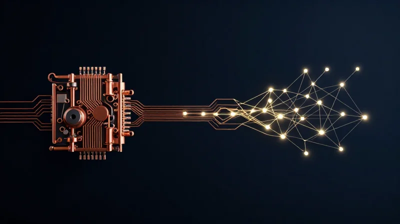
For decades, Printed Circuit Board (PCB) assemblies have served as the backbone of industrial measurement. While reliable for standard applications, these traditional architectures struggle under the weight of modern requirements. The inherent physical constraints—such as signal propagation delays, susceptibility to electromagnetic interference (EMI), and thermal drift—limit their effectiveness in high-bandwidth, high-fidelity data acquisition tasks.
Comparative Performance Metrics
| Feature | Traditional PCB Assembly | Next-Gen High-Precision |
|---|---|---|
| Signal Integrity | Moderate (EMI sensitive) | Superior (High shielding) |
| Thermal Stability | Low (High drift) | High (Active compensation) |
| Sampling Rate | KHz to Low MHz | GHz range |
| Form Factor | Standard/Bulky | Modular/Miniaturized |
Frequently Asked Questions
- Why are PCBs failing to meet modern demands?
Modern sensors produce high-velocity data streams that exceed the trace routing, impedance control, and noise floor tolerances of standard, general-purpose PCB designs. - What defines a 'Next-Gen' measurement technology?
These systems prioritize signal purity, utilizing advanced substrates, integrated photonics, or dedicated FPGA-based signal conditioning to achieve precision far beyond conventional analog-to-digital converters. - Is the transition to new technology necessary for all sectors?
While legacy systems remain adequate for low-frequency monitoring, industries such as aerospace, semiconductor manufacturing, and high-speed robotics require the enhanced resolution that only next-gen platforms provide.
Understanding Traditional PCB Assembly Limitations
Inherent Limitations of Traditional PCB Assemblies
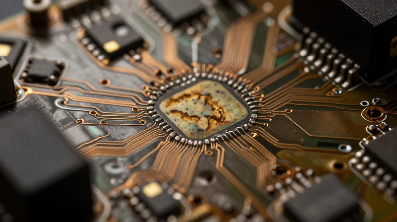
Traditional PCB manufacturing, while reliable for general-purpose electronics, introduces significant hardware constraints when applied to high-precision measurement. These limitations stem from material choices, component mounting techniques, and the thermal properties of standard FR-4 substrates, which often fail to maintain stability under the rigorous demands of modern industrial environments.
Thermal and Signal Integrity Challenges
| Technical Factor | Legacy Limitation | Impact on Precision |
|---|---|---|
| Thermal Expansion | High CTE (Coefficient of Thermal Expansion) | Mechanical stress leads to solder joint failure and drift |
| Signal Noise | Non-optimized trace geometry | Increased parasitic capacitance and crosstalk in sensitive analog paths |
| Stability | Hygroscopic substrate materials | Moisture absorption changes dielectric constant, skewing measurements |
Frequently Asked Questions Regarding PCB Constraints
- Why is FR-4 considered unsuitable for extreme high-precision?
FR-4 is highly sensitive to temperature fluctuations and moisture. These environmental variables alter the board's dielectric constant, causing significant shifts in impedance that degrade sensor calibration. - How does signal noise manifest in traditional assemblies?
Older layout methodologies often lack advanced shielding and multi-layer impedance control, leaving analog signal paths vulnerable to electromagnetic interference and board-level crosstalk. - Does mechanical instability affect accuracy?
Yes; standard surface-mount technologies are prone to fatigue over time. Micro-flexing of the PCB under thermal stress results in localized resistance changes, introducing non-linear errors in data acquisition.
Defining High-Precision PCB Fabrication
Defining High-Precision PCB Fabrication
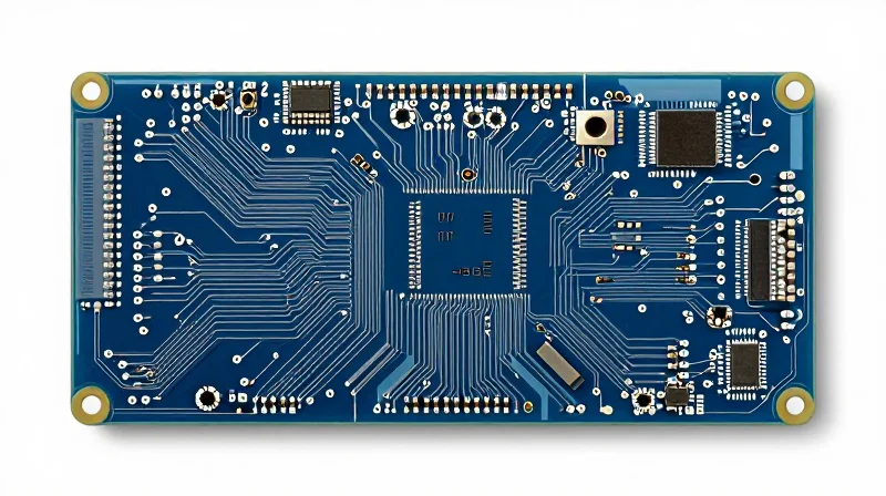
High-precision PCB fabrication is the systematic engineering of circuit boards designed to maintain extreme mechanical and electrical stability under demanding environmental conditions. Unlike standard assemblies, these boards leverage controlled impedance, minimized Coefficient of Thermal Expansion (CTE), and superior signal integrity to support high-frequency and mission-critical applications where legacy manufacturing processes fail to perform.
Critical Pillars of Advanced Fabrication
- Material Selection
Engineers now prioritize low-loss, high-frequency laminates such as PTFE-based composites or ceramic-filled hydrocarbons, which provide consistent dielectric constants across varying temperatures. - Advanced Lamination Processes
Next-gen fabrication employs sequential lamination and precise pressure-temperature profiling to minimize internal stress and ensure absolute registration accuracy in multi-layer board architecture. - Surface Finish Precision
Implementation of Electroless Nickel Immersion Gold (ENIG) or Immersion Silver ensures a planar surface, critical for fine-pitch component mounting and reducing parasitic capacitance.
| Feature | Traditional Assembly | High-Precision Alternative |
|---|---|---|
| Material Stability | Variable with heat | High consistency (low CTE) |
| Lamination Method | Standard mass production | Controlled-pressure/Sequential |
| Signal Integrity | Susceptible to noise | Optimized for high-speed |
Key Considerations for Next-Gen Integration
When transitioning to high-precision alternatives, fabrication must be viewed as an integrated process. The interaction between substrate choice, copper roughness management, and plating uniformity defines the upper limit of measurement accuracy. By focusing on these granular manufacturing parameters, designers can effectively bridge the performance gap between legacy systems and modern, ultra-reliable instrumentation.
Comparative Analysis: Stability and Signal Integrity
Comparative Analysis: Stability and Signal Integrity
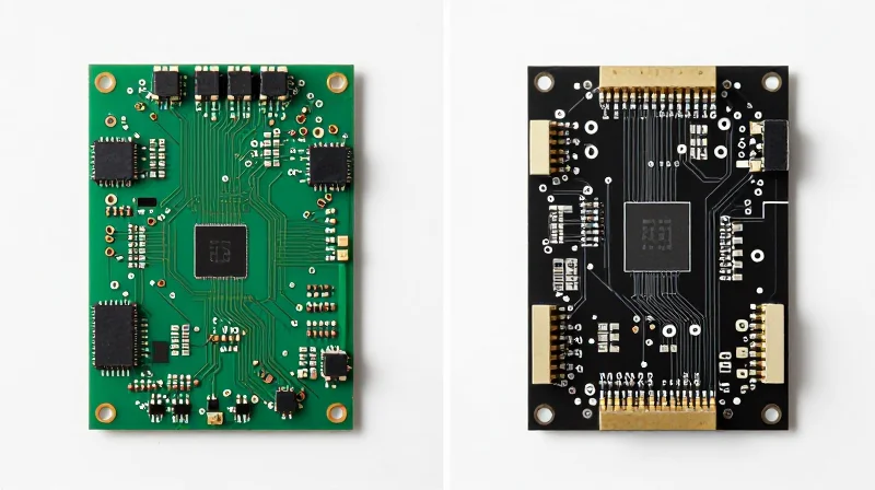
The evolution of measurement technology has necessitated a departure from legacy PCB fabrication to accommodate increasingly sensitive signal chains. While traditional assemblies often struggle with thermal expansion mismatches and parasitic inductance, next-generation high-precision alternatives utilize advanced substrates and precision-controlled manufacturing to minimize noise floor fluctuations and signal degradation.
| Parameter | Traditional PCB Assembly | High-Precision Alternative |
|---|---|---|
| Thermal Coefficient of Expansion | High (Variable) | Ultra-Low (Stable) |
| Signal Noise Floor | Moderate to High | Extremely Low |
| Dielectric Consistency | Standard Tolerance | Precision Controlled |
| Interconnect Integrity | Subject to Stress | Enhanced Reliability |
Key Differentiators in Signal Integrity
High-precision alternatives distinguish themselves through rigorous control over the board's dielectric constant and copper surface roughness. By mitigating these variables, manufacturers can ensure predictable impedance profiles, which are vital for maintaining signal integrity in high-frequency applications.
- How does material selection affect stability?
Next-gen substrates offer significantly lower thermal expansion rates, preventing micro-cracks and impedance shifts that typically plague legacy assemblies under temperature cycles. - What is the primary driver of signal noise in legacy boards?
Signal noise is largely driven by poor substrate homogeneity and inconsistent copper etching, which create parasitic reactive components in the signal path. - Why is structural stability essential for modern measurement?
Modern measurements require consistent phase and amplitude response; high-precision boards ensure that mechanical vibrations and thermal stress do not manifest as measurement errors.
The Role of Advanced Materials in Extreme Environments
Material Science and Environmental Resilience
In extreme environments—characterized by rapid thermal fluctuations and high-frequency vibration—traditional FR-4 substrates often fail due to their high Coefficient of Thermal Expansion (CTE) mismatch with copper traces. Next-gen high-precision alternatives utilize advanced materials such as ceramic-filled PTFE, polyimides, and liquid crystal polymers (LCP). These materials provide superior dimensional stability, lower dielectric loss, and significantly enhanced thermal management properties compared to standard epoxy resins.
Comparison of Substrate Performance in Stressful Environments
| Substrate Type | CTE Stability | Thermal Conductivity | Vibration Resistance |
|---|---|---|---|
| Standard FR-4 | Poor (High expansion) | Low | Low (Delamination risk) |
| High-Tg Polyimide | Moderate | Moderate | High (Flexible base) |
| Ceramic-Filled PTFE | Excellent (Low expansion) | High | Excellent (Rigid) |
Common Challenges in Extreme Deployment
- How does substrate thermal expansion affect data accuracy?
As a board expands during thermal cycling, trace geometry shifts, leading to impedance mismatch and timing jitter. Advanced materials with low CTE minimize these physical deformations, preserving signal timing. - Why is material rigidity important for vibration resistance?
High-vibration environments can induce micro-cracks in solder joints and copper traces. Materials with high elastic moduli and superior bonding properties act as a mechanical buffer, preventing fatigue failures. - Do high-precision materials impact heat dissipation?
Yes. Next-gen alternatives often incorporate thermally conductive fillers that dissipate heat away from critical components faster, preventing localized hot spots that lead to hardware failure.
Manufacturing Precision: The Shift toward Next-Gen Fabrication
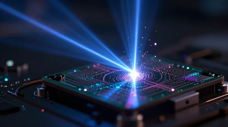
The shift toward next-gen fabrication marks a fundamental departure from mechanical tooling. By transitioning to laser-based drilling and specialized plating techniques, manufacturers have eliminated the physical limitations and variances found in traditional PCB assembly, resulting in tighter tolerances and superior electrical reliability.
Technological Advancements in Fabrication
| Method | Legacy Approach | Next-Gen Advantage |
|---|---|---|
| Drilling | Mechanical Drill Bits | UV & CO2 Laser Systems |
| Interconnects | Thru-Hole Plating | Stacked/Staggered Micro-vias |
| Surface Finish | HASL | ENEPIG & Electroless Gold |
Laser drilling allows for the creation of micro-vias with diameters often smaller than 50 microns. Unlike traditional mechanical bits that suffer from wear and debris, laser systems provide clean, perpendicular walls that significantly enhance signal integrity in high-frequency applications.
Frequently Asked Questions
- Why is laser drilling superior to mechanical drilling?
Laser drilling enables precise aspect ratios for ultra-fine pitch components and micro-vias, which are impossible to achieve consistently with mechanical drills. - How do surface finishes impact signal performance?
Modern finishes like ENEPIG provide superior planarity and corrosion resistance, reducing surface skin effect losses that degrade high-speed signal transmissions. - Does next-gen fabrication increase production costs?
While initial capital expenditure for laser and additive equipment is higher, the reduction in scrap rates and the ability to manufacture high-density interconnect (HDI) boards offset costs through increased yield and performance density.
ROI and Long-Term Market Competitiveness
The Economics of Reliability: From Capex to Opex
While traditional PCB assemblies often present lower upfront capital expenditure, they frequently incur significant hidden costs through calibration drift, signal degradation, and premature system failure. Modern high-precision alternatives utilize advanced materials and manufacturing tolerances that extend the operational lifespan of the hardware. By reducing the frequency of field repairs and decreasing the necessity for frequent system recalibration, organizations realize a lower Total Cost of Ownership (TCO) that justifies the initial premium.
| Metric | Traditional Assemblies | High-Precision Alternatives |
|---|---|---|
| Calibration Frequency | High/Frequent | Low/Stable |
| Mean Time Between Failures | Standard | Extended by 30-50% |
| Maintenance Labor Cost | High | Minimal |
| Performance Predictability | Variable | High/Consistent |
Securing Market Competitiveness Through Precision
In highly regulated industries such as medical diagnostics, aerospace, and autonomous robotics, precision is a core value proposition. Next-gen fabrication allows for tighter signal integrity and lower noise floors, enabling equipment to meet rigorous industry standards that traditional boards cannot sustain over time. This performance reliability becomes a critical competitive advantage, allowing manufacturers to market their products as 'install-and-forget' solutions that guarantee uptime for end-users.
Strategic FAQ
- Does the higher cost of next-gen PCBs hinder scalability?
No, it enhances it. The reduction in warranty claims and field support requirements scales positively, as the cost of supporting a reliable, high-spec product is significantly lower than managing a fleet of legacy hardware experiencing frequent outages. - How does PCB precision influence market entry?
Next-gen boards enable performance capabilities—such as higher frequency operation or smaller form factors—that were previously impossible, allowing companies to enter premium niches with higher profit margins.
Best Practices for Transitioning Your Hardware Roadmap
Transitioning from legacy PCB assemblies to high-precision, next-gen hardware is not merely a component swap; it is a fundamental shift in design philosophy. To remain competitive, engineering teams must move beyond traditional design rules toward a holistic fabrication strategy that prioritizes signal integrity, thermal stability, and mechanical precision from the early conceptual phases.
Strategic Phasing for Roadmap Transition
| Transition Phase | Primary Objective | Key Engineering Action |
|---|---|---|
| Evaluation | Identify performance bottlenecks | Conduct signal integrity and thermal stress analysis. |
| Prototyping | Validate next-gen tolerances | Engage fabrication partners for micro-via feasibility. |
| Implementation | Optimize for volume | Refine design-for-manufacturing (DFM) rules. |
Key Considerations for Engineering Teams
- How do I mitigate supply chain risks during transition?
Partner with fabricators early who offer dual-capability in both traditional and high-precision lines to ensure a fallback option during the certification of new processes. - What is the biggest pitfall in shifting to high-precision assemblies?
Underestimating the change in material characteristics, such as CTE (Coefficient of Thermal Expansion), which requires recalibration of your entire enclosure and thermal management stack. - Should we move the entire product line at once?
No. Adopt a 'pilot-platform' approach, transitioning your most performance-sensitive module first to establish new design benchmarks before retrofitting legacy systems.
By treating this transition as an iterative roadmap evolution rather than a one-time project, firms can minimize development downtime. Focus on establishing robust design rules that leverage modern laser-drilling and surface-finishing techniques to ensure that every transition phase yields measurable improvements in reliability and measurement precision.
Transitioning to high-precision PCB technology is no longer a luxury—it is a prerequisite for industry leaders demanding superior measurement reliability. By moving away from legacy assembly constraints, you secure higher accuracy and long-term product viability. Ready to elevate your design standards? Contact our engineering team today for a comprehensive consultation on your next project.
