
As the demand for ultra-compact consumer electronics surges, the limitations of traditional Surface Mount Technology (SMT) are becoming increasingly apparent. For hardware engineers, the shift to micro-BGA (Ball Grid Array) architectures is not just a trend—it is a necessity for maintaining high-density, high-performance designs. This article explores the evolution of assembly, the technical hurdles of miniaturization, and the advanced inspection strategies required to ensure reliability in the next generation of electronics.
The Declining Efficiency of Traditional SMT

The Scaling Ceiling of Traditional SMT
Traditional Surface Mount Technology has long served as the industry standard, yet it is currently hitting a critical physical limit defined by lead pitch and parasitic resistance. As Integrated Circuits (ICs) transition toward sub-nanometer nodes, the physical dimensions of traditional SMT packages cannot match the footprint reduction required by high-density interconnects. The primary issue lies in the reliance on peripheral lead configurations, which suffer from signal integrity degradation at high frequencies and mechanical stress vulnerabilities during thermal cycling.
Comparative Efficiency Metrics
| Feature | Traditional SMT (QFP/SOIC) | Micro-BGA/CSP |
|---|---|---|
| Pin Density | Low to Moderate | Very High |
| Signal Integrity | Susceptible to EMI/Crosstalk | Optimized Ground Planes |
| Assembly Footprint | Large relative to die size | Near-chip-scale (CSP) |
| Thermal Path | High thermal resistance | Low-impedance thermal via array |
Technical Bottlenecks in High-Density Interconnects
- Why does lead pitch affect performance?
As pin density increases, the reduction in pitch leads to 'bridge' defects during soldering and increased parasitic capacitance, which limits high-speed data throughput. - How do signal paths impact reliability?
Longer lead frames in traditional SMT packages act as antennas for electromagnetic interference, while the mechanical cantilever effect of peripheral leads makes them prone to fatigue under repetitive thermal stress. - Is SMT viable for modern ultra-thin devices?
Due to the z-height constraints and inability to utilize the underside of the package, traditional SMT is increasingly unsuited for the form factors of modern mobile and IoT applications.
The transition to Micro-BGA is not merely a preference but a technological necessity to overcome these impedance mismatches. By replacing vulnerable peripheral leads with an area array of solder balls, Micro-BGA architectures significantly shorten the electrical path, effectively lowering inductance and enabling cleaner signal paths essential for next-generation system-on-chip (SoC) integration.
Understanding Micro-BGA Architectures
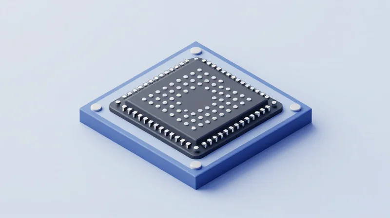
Micro-BGA (Ball Grid Array) architectures have fundamentally redefined high-density interconnects by transitioning away from peripheral lead-frame connections to a high-density area array. By utilizing solder bumps directly on the bottom surface of the die or substrate, these packages eliminate the parasitic resistance and inductance associated with traditional wire-bonding, facilitating the miniaturization required for modern mobile and wearable ecosystems.
Structural Advantages of Micro-BGA
| Feature | Traditional SMT (QFP/SOIC) | Micro-BGA |
|---|---|---|
| Pin Pitch | 0.5mm - 0.8mm | 0.2mm - 0.4mm |
| Electrical Path | Long wire bonds | Short solder bumps (Flip-chip) |
| Thermal Path | Primary through leads | Primary through substrate and bumps |
| Footprint | Large, peripheral-only | Compact, area array |
Critical Performance Drivers
- Why does Micro-BGA improve signal integrity?
The shortened interconnect length between the silicon die and the PCB significantly reduces inductance and capacitance, allowing for faster switching speeds and reduced signal cross-talk in high-frequency applications. - How does Micro-BGA impact wearable design?
By shifting the interconnect density to an area array rather than a single perimeter, developers can route high-speed signals under the component body, freeing up significant board real estate for battery and sensor integration. - What is the role of underfill in these architectures?
Due to the Coefficient of Thermal Expansion (CTE) mismatch between the silicon die and the organic substrate, an epoxy underfill is essential to redistribute mechanical stress during thermal cycling, preventing solder joint fatigue.
As portable devices demand ever-increasing processing power within restricted dimensions, the transition to Micro-BGA is no longer optional but mandatory for thermal management and signal routing efficiency. Future iterations continue to push the boundaries of pitch reduction, moving toward fine-pitch BGA (fBGA) to accommodate the massive I/O counts necessitated by modern System-on-Chip (SoC) designs.
Technical Challenges in Miniaturized Assembly
Critical Engineering Challenges in Micro-BGA Integration
As micro-BGA footprints shrink below 0.5mm pitch, the physical tolerances for manufacturing decrease exponentially. The primary challenge lies in achieving reliable solder joint formation without bridge defects, coupled with the management of thermal gradients that can jeopardize the structural integrity of the thin substrates used in high-density applications.
Reflow and Thermal Management Constraints
Micro-BGA assembly demands hyper-precise temperature control during reflow. Because the thermal mass of individual solder balls is exceptionally low, excessive soak times can lead to premature oxidation or 'head-in-pillow' (HIP) defects. Furthermore, the high density of interconnects often requires advanced underfill materials to redistribute the coefficient of thermal expansion (CTE) stresses, preventing fatigue-induced fractures during operational thermal cycling.
| Challenge Area | Micro-BGA Impact | Traditional SMT Comparison |
|---|---|---|
| Solder Volume Control | Extreme sensitivity; requires precise jetting | High tolerance for standard paste printing |
| Thermal Dissipation | High localized heat density; requires vias | Easier distribution due to larger surface area |
| Inspection Integrity | Requires 3D X-Ray/AOI for hidden joints | Visual inspection often sufficient |
- What is the greatest risk in micro-BGA reflow?
The greatest risk is the formation of 'head-in-pillow' defects, where the solder ball fails to fully coalesce with the PCB pad due to warpage or insufficient flux activation. - How does underfill affect reliability?
Underfill encapsulates the solder joints, providing mechanical support that minimizes the impact of CTE mismatches between the silicon die and the PCB substrate. - Why is traditional SMT inspection failing for micro-BGA?
Because the joints are positioned underneath the component, optical inspection cannot verify the inner solder connections, necessitating expensive 3D X-ray systems.
Transitioning from Traditional SMT to Micro-BGA
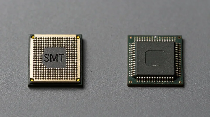
Strategic Shifts in Assembly Requirements
Moving from traditional Surface Mount Technology (SMT) to micro-BGA architectures involves more than just changing component types; it demands a comprehensive recalibration of the SMT line. As package pitches shrink below 0.5mm, the margin for error in solder paste deposition and component alignment narrows significantly, necessitating high-accuracy vision systems and refined material selection.
| Parameter | Traditional SMT | Micro-BGA Assembly |
|---|---|---|
| Placement Accuracy | ±50 microns | ±10-15 microns |
| Solder Paste Control | Standard Stencils | Nano-coated/Laser-cut Stencils |
| Inspection Method | AOI (Visual) | Automated X-Ray Inspection (AXI) |
| Thermal Profile | Standard Ramp-Soak | Optimized Low-Voiding Profile |
Process Control and Material Evolution
The transition necessitates a shift toward Type 4 or Type 5 solder pastes to accommodate the finer aperture requirements of micro-BGA pads. Furthermore, board finishes must be strictly controlled; Electroless Nickel Immersion Gold (ENIG) or Immersion Silver are preferred over HASL to ensure a perfectly flat landing surface, which is critical for consistent joint formation at the micro-scale.
Frequently Asked Questions Regarding Transition
- Can existing SMT lines handle micro-BGA?
Most high-end SMT lines can be upgraded, but they often require precision feeders, enhanced vision software for fiducial recognition, and potentially an inline AXI machine to verify hidden solder joints. - Why is X-Ray inspection mandatory for micro-BGA?
Because the solder balls are located underneath the package, optical inspection cannot verify joint integrity or detect internal voids, making AXI the only reliable method for quality control. - Does micro-BGA assembly increase thermal stress?
Yes, the smaller solder volumes are more susceptible to thermal fatigue. Proper reflow profiling is essential to minimize voiding and maximize the mechanical life of the interconnects.
Evolution of Advanced Inspection Technologies

The Shift Beyond Optical Limitations
As micro-BGA components scale down, traditional 2D Automated Optical Inspection (AOI) has reached its physical limits. These packages, often featuring pitch dimensions below 0.3mm, hide critical solder connections beneath the silicon die, rendering them invisible to standard camera systems. Modern inspection requires a paradigm shift toward volumetric analysis and subsurface imaging to identify defects like micro-voiding, head-in-pillow joints, and subtle misalignments that cause intermittent failures.
Advanced Inspection Modalities Compared
| Technology | Primary Application | Detection Capability |
|---|---|---|
| 2D AOI | Surface Component Alignment | Surface defects, missing parts, polarity |
| 3D AOI | Solder Paste & Component Height | Coplanarity, volume, lead lifting |
| 3D AXI (X-Ray) | Micro-BGA Solder Joints | Voids, bridging, head-in-pillow, internal shorts |
Key Questions in Advanced Inspection
- Why is 3D AXI essential for micro-BGA?
3D Automated X-ray Inspection allows for 'slice-based' imaging, enabling engineers to inspect specific layers within the BGA stack to confirm internal solder joint integrity without being obscured by other layers. - What role does AI play in modern inspection?
AI-driven algorithms are now being integrated into AOI platforms to reduce false-call rates and autonomously learn from historical defect data, improving detection accuracy for complex micro-scale geometries. - How do micro-voids impact long-term reliability?
While minor voiding is sometimes acceptable, excessive micro-voids reduce the conductive cross-section of the joint, increasing impedance and creating stress concentration points that lead to premature thermal fatigue.
Integrating these technologies into the production line represents a move toward closed-loop manufacturing. By correlating real-time inspection data back to pick-and-place and reflow parameters, manufacturers can dynamically adjust processes, effectively catching drift before it results in significant yield loss.
Reliability and Failure Analysis in High-Density Interconnects
Reliability and Failure Analysis in High-Density Interconnects
As interconnect densities scale downward, traditional reliability metrics are insufficient for capturing the complex failure modes inherent in Micro-BGA assemblies. Maintaining high MTBF (Mean Time Between Failures) necessitates a transition from reactive troubleshooting to predictive failure analysis, leveraging accelerated life testing and multi-physics simulation to identify latent vulnerabilities in solder joint integrity and intermetallic compound (IMC) growth.
Core Reliability Challenges
The primary risks for high-density packages stem from thermomechanical fatigue and interfacial brittleness. Because Micro-BGA joints occupy significantly smaller volumes, the cumulative effects of thermal cycling—exacerbated by coefficient of thermal expansion (CTE) mismatches—can lead to crack propagation that is virtually undetectable through conventional functional testing.
| Failure Mode | Primary Trigger | Detection Strategy |
|---|---|---|
| Solder Joint Cracking | Thermal Cycling | Temperature Cycling & Shear Testing |
| IMC Embrittlement | Excessive Reflow Time | Cross-sectional SEM Analysis |
| Micro-Voiding | Solder Paste Volatility | 3D Automated X-Ray Inspection |
Advanced Failure Analysis Protocols
- How does Scanning Electron Microscopy (SEM) enhance analysis?
SEM provides high-resolution imaging of intermetallic growth at the solder-substrate interface, allowing engineers to determine if brittle fracture risks are present before mass production. - What role does Finite Element Analysis (FEA) play?
FEA models simulate physical strain distribution across the BGA array under operational thermal loads, enabling design adjustments in pad geometry or package substrate material prior to physical prototyping. - Why is Accelerated Life Testing (ALT) critical?
ALT compresses years of environmental stress into weeks, identifying failure precursors such as creep deformation and oxidative degradation that define the effective MTBF of the device.
Ultimately, a robust failure analysis framework must integrate real-time monitoring of electrical resistance during thermal cycling to catch transient intermittent failures. By correlating structural anomalies identified in 3D X-ray with long-term reliability performance, manufacturers can establish a feedback loop that continually refines reflow profiles and material specifications for next-generation micro-electronics.
Future-Proofing Your PCB Design Strategy
The Scalability Paradigm: Moving Beyond Static DFM
Modern hardware engineering can no longer rely on static design rules. To remain competitive as micro-BGA packages continue to shrink in pitch and increase in I/O count, engineers must adopt dynamic DFM standards that evolve with assembly capabilities. Future-proofing entails moving from 'design for assembly' toward 'design for repeatability,' ensuring that high-yield outcomes are baked into the layout before fabrication begins.
Strategic Comparison: Traditional SMT vs. Micro-BGA DFM
| Design Criterion | Traditional SMT Strategy | Micro-BGA Scalability Strategy |
|---|---|---|
| Via Technology | Thru-hole; Standard plating | HDI (Micro-vias); Via-in-pad |
| Thermal Management | Copper pours and heat sinks | Thermal micro-vias; Substrate thermal vias |
| Tolerance Buffers | Generous pads; Loose alignment | Optimized solder masks; Laser direct imaging |
| Inspection | 2D Optical; Manual checks | 3D X-Ray; Automated AOI with AI |
Key Considerations for Future-Proofing
- Why is predictive modeling essential?
Early-stage simulation of thermal stress and signal integrity allows designers to preemptively identify failure points in micro-BGA connections before physical prototyping. - How does digital supply chain integration impact design?
Collaborating with CMs (Contract Manufacturers) through digital manufacturing twins ensures that your design choices remain within the current capabilities of high-end assembly lines. - What role does material selection play?
Moving toward low-loss, high-glass-transition-temperature (Tg) materials is critical to maintaining mechanical stability as micro-BGA components increase in density and heat output.
Ultimately, the shift toward future-proof design is a commitment to continuous learning. By leveraging AI-driven inspection data to feed back into the CAD environment, engineers can create a closed-loop system where manufacturing hurdles directly refine future design templates. This iterative approach not only shortens time-to-market but establishes a robust defense against the risks of obsolescence in the high-density electronics landscape.
The transition to micro-BGA is essential for engineers aiming to stay ahead in the rapidly evolving consumer electronics market. By prioritizing advanced inspection and robust design protocols, you can overcome the limitations of traditional SMT and deliver reliable, high-density products. Contact our engineering team today to optimize your next PCB design for the future of micro-packaging.
