
As global data traffic continues its exponential climb, the physical infrastructure of our network backbone is undergoing a radical transformation. Engineers are no longer merely asking how to add more bandwidth, but how to do so with greater energy efficiency and density. This article examines the technological shift from traditional PCBA-based optical transceivers toward integrated silicon photonics, revealing how this transition is set to define the next decade of high-speed connectivity.
The Evolution of Optical Networking
From Discrete Components to Pluggable Modules
The foundational era of optical networking relied heavily on discrete component assembly. Engineers utilized individual lasers, modulators, and detectors, each housed in its own package and interconnected via complex printed circuit board assemblies (PCBA). This traditional approach provided the flexibility to iterate on specific optical functions independently but introduced significant bottlenecks as bandwidth demands skyrocketed.
The Limitations of Legacy PCBA Integration
Traditional PCBA-based transceivers face physical and economic ceilings. As data rates pushed toward 400G and 800G, the challenges of manual alignment, signal integrity across interconnects, and cooling density became primary constraints on scaling.
| Constraint | Legacy PCBA Impact | Scaling Barrier |
|---|---|---|
| Component Alignment | Manual active alignment required | High labor costs/low throughput |
| Interconnect Loss | Signal degradation over copper traces | Distance/bandwidth limitations |
| Footprint | Bulky discrete packaging | Density limits in switch ASICs |
Frequently Asked Questions
- Why did traditional PCBA manufacturing hit a wall?
As data speeds increased, the electrical trace length between the optical engine and the DSP caused signal loss, and the physical size of discrete components prevented higher port density on switches. - How does silicon photonics differ from legacy designs?
Silicon photonics leverages standard CMOS fabrication processes, allowing optical components to be etched directly onto silicon wafers, dramatically reducing size and enabling monolithic integration.
Anatomy of Traditional Optical Transceiver PCBA
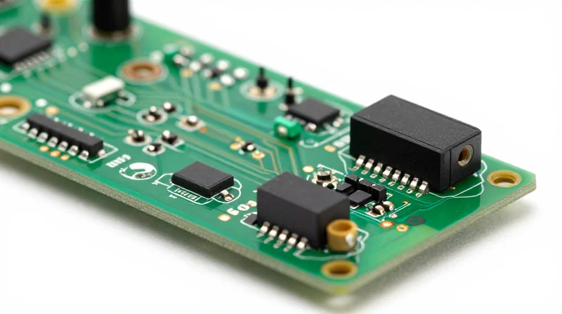
Discrete Architecture and Component Interconnects
A traditional optical transceiver PCBA is defined by a discrete component architecture where individual sub-assemblies—such as lasers (DFB or EML), modulators, photodetectors, and drivers—are mounted onto a ceramic or organic substrate. These components are interconnected via wire bonds or flexible circuits, creating a highly modular but physically bulky signal path.
The reliance on manual or semi-automated pick-and-place processes for discrete optical coupling introduces inherent alignment tolerances. Each optical interface requires precise lens alignment to focus light into the fiber, a process that is not only time-intensive but also represents a primary failure point regarding signal integrity and physical vibration resistance.
Critical Performance Bottlenecks
| Bottleneck Category | Primary Challenge | Impact on Scalability |
|---|---|---|
| Physical Footprint | Discrete packaging size | High density board congestion |
| Thermal Management | High thermal resistance paths | Power consumption limits |
| Signal Integrity | Parasitic inductance of wire bonds | Bandwidth ceiling at higher baud rates |
- Why do wire bonds limit frequency scaling?
Wire bonds introduce parasitic inductance and capacitance that degrade electrical signal quality at high frequencies, effectively capping the maximum data rate per channel. - How does discrete mounting affect heat dissipation?
Each component interfaces with the PCB through distinct thermal impedance paths, leading to localized 'hot spots' that struggle to dissipate heat effectively in high-density rack environments. - Is automation a viable solution for current designs?
While modern SMT lines are highly efficient, the sub-micron accuracy required for optical coupling necessitates complex active alignment, which remains a costly and throughput-limiting step in production.
The Rise of Silicon Photonics: A Paradigm Shift
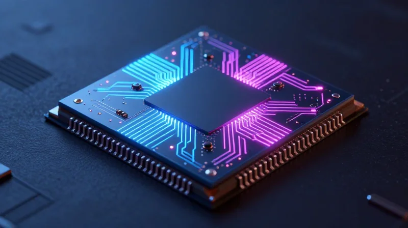
The Essence of Silicon Photonics
Silicon photonics represents a migration from discrete, manually assembled optical components to highly integrated, monolithic architectures. By leveraging mature CMOS (Complementary Metal-Oxide-Semiconductor) fabrication processes, engineers can now embed optical waveguides, modulators, and photodetectors directly into silicon wafers. This paradigm shift replaces the cumbersome 'pick-and-place' assembly of traditional transceiver PCBAs with photolithography, allowing for the precise, mass-scale production of complex optical circuits that were previously impossible to miniaturize.
Core Advantages of On-Chip Integration
The primary driver for this shift is the drastic reduction in physical footprint and power consumption. In traditional designs, signal loss occurs at every interface between components—lasers, lenses, and fibers. Silicon photonics minimizes these transition zones by keeping the signal within the silicon substrate. Furthermore, the ability to pack thousands of optical functions into a square millimeter drastically increases the bandwidth density required for modern AI and data center interconnects.
| Feature | Traditional PCBA | Silicon Photonics |
|---|---|---|
| Manufacturing | Discrete Component Assembly | CMOS Photolithography |
| Scalability | Limited by Size/Complexity | High-Density Integration |
| Power Efficiency | High (Interface Losses) | Low (Integrated Circuitry) |
Frequently Asked Questions
- Does silicon photonics eliminate the need for lasers?
No, silicon is not naturally efficient at emitting light. Instead, external light sources are coupled into the silicon photonic chip, which then handles the modulation and routing. - Why is CMOS manufacturing critical to this shift?
CMOS compatibility allows optical components to be produced in the same high-volume semiconductor foundries as logic chips, drastically lowering costs and increasing reliability through standard wafer-level processes.
Comparing Efficiency and Power Consumption
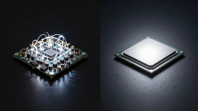
Efficiency Gains Through Integration
The primary driver for the migration toward silicon photonics is the radical reduction in power consumption achieved by collapsing bulky discrete optical components into monolithic or co-packaged silicon structures. Traditional optical transceivers rely on individual laser diodes, modulators, and detectors that require complex electrical interconnects across a printed circuit board (PCB). These connections introduce parasitic capacitance and resistance, forcing drivers to expend significant energy just to overcome signal attenuation.
In contrast, silicon photonics integrates these elements at the nanometer scale. By shortening the physical path between the CMOS control logic and the photonic components, developers can operate at lower drive voltages and significantly reduce signal integrity overhead. This transition is not merely incremental; it enables a new generation of data centers to handle hyperscale workloads without proportional scaling in thermal cooling requirements.
Performance Comparison Matrix
| Metric | Traditional PCBA | Silicon Photonics |
|---|---|---|
| Power-per-bit (pJ/bit) | 15 - 25 pJ/bit | 3 - 8 pJ/bit |
| Thermal Density | High (Discrete components) | Low (Monolithic integration) |
| Signal Path Length | Centimeters | Micrometers |
| Scaling Potential | Limited by board space | High (CMOS-compatible) |
Key Considerations in Power Management
- Why does integration lower power consumption?
By eliminating discrete electrical interconnections, the system reduces the load on high-speed drivers, directly lowering the energy required to transmit each bit of data. - How does CMOS compatibility affect efficiency?
Leveraging existing semiconductor fabrication processes allows for the tight co-packaging of electronics and photonics, minimizing the impedance mismatch that typically plagues traditional optical PCB assemblies. - Is heat dissipation the main bottleneck?
Yes; as port densities increase, traditional PCBAs face thermal throttling limits, whereas silicon photonics' reduced power-per-bit profile allows for significantly higher bandwidth densities within the same thermal envelope.
Scalability and Manufacturing Cost Dynamics
The Economic Shift: CMOS Foundries vs. Discrete Assembly
The primary driver behind the transition to silicon photonics is the leveraging of high-volume complementary metal-oxide-semiconductor (CMOS) foundry infrastructure. Traditional optical transceiver PCBA manufacturing relies on labor-intensive, precision assembly of discrete lasers, modulators, and photodetectors. This approach scales linearly with cost, as each component requires independent alignment and packaging. In contrast, silicon photonics permits the integration of these functions onto a single silicon die, enabling wafer-level manufacturing that benefits from the established economies of scale found in the semiconductor industry.
| Feature | Traditional PCBA | Silicon Photonics |
|---|---|---|
| Manufacturing Model | Discrete assembly/alignment | Wafer-scale CMOS integration |
| Scaling Potential | Low (Linear cost) | High (Exponential cost reduction) |
| Packaging Complexity | High (Multi-die/Fiber alignment) | Medium (Photonic/Electronic co-packaging) |
| Capex Requirements | Moderate (High tooling/Labor) | High (Foundry/Equipment access) |
Scalability and Cost Dynamics FAQ
- How does silicon photonics achieve lower long-term manufacturing costs?
By utilizing existing CMOS infrastructure, manufacturers can move from manual piece-part assembly to automated lithographic patterning, significantly increasing throughput and reducing labor costs per unit. - Does higher initial Capex hinder the adoption of silicon photonics?
While the setup for silicon photonics manufacturing is capital-intensive due to advanced lithography and testing requirements, the cumulative cost savings at high volumes (millions of units) far outweigh the initial investment compared to discrete PCBA methods. - What remains the biggest challenge in silicon photonics production?
The most significant hurdle is the coupling and packaging interface—specifically, the efficient attachment of optical fibers to the silicon die and the integration of heterogeneous laser sources onto the silicon substrate.
Ultimately, the shift is not merely technical but economic. As data centers push toward terabit-per-second connectivity, the cost-per-gigabit of traditional PCBA-based modules becomes unsustainable due to inherent component count and assembly overhead. Silicon photonics addresses this by consolidating functionality into a smaller, standardized footprint, setting the stage for commoditized high-speed optical networking.
Overcoming Integration Challenges

Addressing the Silicon Photonics Integration Gap
While silicon photonics offers transformative potential for high-bandwidth connectivity, its adoption faces significant engineering friction compared to established PCBA transceiver techniques. The primary challenge remains the monolithic integration of light sources on silicon, which lacks an inherent direct-bandgap structure. Developers must now navigate the complexities of heterogeneous integration and precise sub-micron alignment to achieve reliable performance at scale.
Core Technical Challenges and Mitigations
| Challenge | Silicon Photonics Impact | Standard PCBA Mitigation |
|---|---|---|
| Laser Integration | Requires bonding of III-V materials | Well-established discrete components |
| Optical Coupling | High sensitivity to misalignment | Standard fiber-to-lens alignment |
| Thermal Sensitivity | High thermal drift in silicon waveguides | Stable PCB-based thermal management |
Frequently Asked Questions
- Why is laser integration difficult in silicon photonics?
Silicon is an indirect-bandgap material, making it inherently inefficient at emitting light. Integration currently requires complex heterogeneous bonding of III-V semiconductor materials, such as Indium Phosphide, onto the silicon substrate. - How does thermal management differ from traditional PCBAs?
Silicon waveguides are extremely sensitive to temperature variations, which shift the refractive index and disrupt optical performance. Unlike standard PCBAs, silicon photonics systems require sophisticated thermal monitoring and active micro-heaters to maintain wavelength stability. - What is the status of coupling efficiency in modern designs?
Advancements in grating couplers and edge couplers have significantly reduced insertion losses. However, the high-precision alignment required for mass production remains a bottleneck compared to the robust, tolerant assembly processes of traditional transceivers.
Performance Benchmarks in Hyperscale Data Centers
Performance Benchmarks in Hyperscale Deployments
As data traffic growth outpaces Moore’s Law, the industry is shifting from discrete optical components toward monolithic Silicon Photonics (SiPh). In hyperscale environments, where thousands of links connect spine-leaf architectures, the power penalty and physical footprint of traditional pluggable transceivers have become a critical bottleneck.
| Metric | Traditional PCBA (800G) | Silicon Photonics (800G) |
|---|---|---|
| Power Consumption (pJ/bit) | 12 - 15 | 6 - 8 |
| Reach Capabilities | Up to 10km | Extended via Co-Packaging |
| Form Factor Complexity | High (Discrete parts) | Low (Integrated CMOS) |
| Throughput Density | Limited by Heat | Extreme (Higher Integration) |
Efficiency Drivers in Photonic Integration
Silicon photonics reduces the distance electrons must travel to modulate light. By co-packaging the photonic integrated circuit (PIC) directly with the switch ASIC, hyperscalers reduce the signal path latency and thermal dissipation requirements. This move eliminates the need for power-hungry re-timers and long PCB traces that currently dominate the energy budget of standard pluggable modules.
Frequently Asked Questions
- Why do SiPh modules consume less power?
They minimize the electrical-to-optical conversion overhead by utilizing CMOS-compatible manufacturing, which allows for deeper integration of drivers and modulators on a single die. - Can SiPh replace traditional transceivers today?
Current hyperscale deployments are shifting toward co-packaged optics (CPO) for high-radix switches, though pluggable SiPh transceivers remain the primary standard for general-purpose networking. - What is the primary constraint of current SiPh designs?
Laser reliability and the efficiency of optical coupling (fiber-to-chip) remain the most significant challenges compared to the mature assembly processes of traditional PCB-based transceivers.
The Roadmap to 800G and Beyond

The 800G Threshold and the Physics of Scaling
As data centers transition to 800G and prepare for 1.6T, traditional PCBA-based transceivers are encountering the 'wall' of signal integrity and power density. While high-end DSPs continue to improve, the physical constraints of electrical traces on PCBs lead to significant insertion loss and thermal bottlenecks. Silicon Photonics (SiPh) offers the necessary leap by moving the optical engine closer to the ASIC, or co-packaging it, significantly reducing the electrical power budget required to move data across high-speed SerDes lanes.
Comparative Trajectories: PCBA vs. Silicon Photonics
| Feature | Traditional PCBA | Silicon Photonics |
|---|---|---|
| Form Factor | Pluggable (QSFP-DD/OSFP) | Co-packaged or Chiplet-based |
| Integration Density | Medium/Limited | Very High (Monolithic) |
| Power Efficiency | Baseline | High (Reduced SerDes Reach) |
| Scaling Outlook | Diminishing Returns at >1.6T | Ready for Terabit+ Scaling |
Strategic Outlook for Next-Generation Networking
The industry is not abandoning traditional PCBA immediately; rather, it is bifurcating. Pluggable transceivers will continue to dominate edge and enterprise environments where flexibility is paramount. However, for massive AI clusters and Hyperscale backbones, the roadmap clearly favors SiPh. By integrating the photonic layer directly into the silicon substrate, manufacturers can bypass the parasitic losses associated with legacy PCB interfaces, essentially enabling the performance required to sustain the next decade of traffic growth.
Frequently Asked Questions
- Will Silicon Photonics completely replace PCBA?
No. PCBA-based optics remain the most cost-effective solution for short-reach, pluggable applications, while SiPh will capture the high-bandwidth, low-latency market in hyperscale computing. - What is the biggest hurdle for 1.6T systems?
The primary barrier is the power consumption of the DSP. Moving to co-packaged optics (CPO) via SiPh allows for shorter electrical links, drastically reducing the energy needed for signal amplification. - How does CMOS manufacturing impact this transition?
Leveraging existing CMOS foundry infrastructure allows SiPh to benefit from the same economies of scale that drove the PC and mobile industries, making large-scale production of integrated optical engines viable.
While traditional transceivers remain the workhorses of current networks, the advantages of silicon photonics in density, cost, and power efficiency are becoming impossible to ignore. For architects building the next generation of data infrastructure, the shift is not just inevitable—it is necessary for sustainable growth. Contact our engineering team today to learn how we can help you integrate advanced optical solutions into your next project.
