
As diagnostic imaging technology pushes into the realm of 7T and beyond, the invisible barriers of traditional electronic design are becoming increasingly prominent. For engineers designing medical devices, the choice of substrate and material composition is no longer just about functionality—it is about managing the intense, unrelenting magnetic fields that can turn standard components into sources of interference. This article explores why the industry is pivoting toward specialized non-magnetic PCB solutions to ensure the reliability of next-generation diagnostic equipment.
The Impact of High-Tesla Environments on PCB Integrity

The Physics of Magnetic Interference
In high-Tesla environments, such as 3T or 7T MRI systems, traditional Printed Circuit Boards (PCBs) act as significant sources of electromagnetic interference and physical instability. Standard electronics often rely on ferritic materials—such as steel-core inductors, nickel-plated connectors, and iron-based fasteners—which experience powerful Lorentz forces when exposed to static magnetic fields. These forces can cause mechanical micro-vibrations, resulting in image artifacts (ghosting), component shear, or catastrophic failure of the diagnostic system's RF coils.
Material Sensitivity Comparison
| Component Type | Traditional Material | MRI Impact | Non-Magnetic Alternative |
|---|---|---|---|
| Fasteners/Bolts | Zinc-plated Steel | High attraction; projectile risk | Phosphor bronze or Titanium |
| Connectors | Nickel-plated Brass | Distorts RF signal; eddy currents | Gold-plated Beryllium Copper |
| Inductors | Ferrite Core | Core saturation; signal noise | Air-core coils |
Frequency Asked Questions on Magnetic Compatibility
- Why is nickel plating considered a failure point in MRI environments?
Nickel is ferromagnetic and becomes magnetized in high-Tesla fields. This creates localized distortion in the magnetic homogeneity of the MRI bore, resulting in severe image artifacts. - How do eddy currents impact PCB trace integrity?
In high-gradient magnetic fields, conductive traces on a PCB can experience induced eddy currents. These currents generate internal heat and opposing magnetic fields that interfere with the diagnostic signal acquisition. - Is stainless steel always safe for PCB assemblies in MRI?
No. Many common grades of stainless steel (like 304 or 400 series) exhibit varying levels of magnetism. Only specific 'MRI-safe' grades are acceptable, though non-ferrous alloys remain the industry standard for high-performance imaging.
Limitations of FR-4 and Standard Conductive Materials
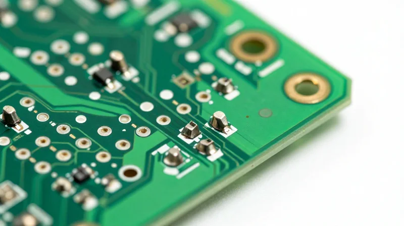
The Material Mismatch: Why Traditional PCBs Fail
While FR-4 (glass-reinforced epoxy laminate) is the workhorse of the electronics industry, it is inherently ill-suited for the specialized requirements of high-field MRI systems. The primary failure mode stems from the presence of ferromagnetic trace elements and the physical dielectric properties that can shift under sustained magnetic pressure. Standard PCB manufacturing often introduces trace amounts of nickel or steel—either in plating layers or through component leads—which act as focal points for mechanical stress and image-distorting artifacts.
Common Failure Points in Diagnostic Imaging Hardware
| Material Component | Issue | Imaging Impact |
|---|---|---|
| Standard Solder | Ferrous contamination | Magnetic field distortion |
| FR-4 Laminate | Outgassing/Instability | Signal-to-noise degradation |
| Nickel Plating | High magnetic susceptibility | Strong eddy current heating |
| Ferrite Beads | Magnetic saturation | Local field inhomogeneity |
Frequently Asked Questions
- Why is nickel plating problematic in MRI machines?
Nickel is highly ferromagnetic, meaning it responds strongly to magnetic fields. In an MRI bore, nickel plating on PCB contacts can experience significant mechanical torque and create localized magnetic field gradients that degrade the quality of the image. - Does FR-4 cause signal interference?
While the dielectric itself is non-conductive, standard manufacturing processes for FR-4 sometimes leave metallic particulates embedded in the laminate, which can cause minor signal noise and thermal expansion issues during active imaging cycles. - What is the primary risk of using traditional ferritic components?
Components containing iron or ferrite cores can saturate in high-Tesla fields, leading to the heating of the component and potential structural failure due to magnetic attraction forces.
Defining Non-Magnetic PCB Solutions
Core Principles of Non-Magnetic PCB Architecture
Achieving non-magnetic performance requires a rigorous purge of all ferromagnetic materials from the assembly stack. This process goes beyond mere component selection, extending into the molecular level of laminates and the electrochemical nature of plating baths, ensuring that the assembly remains magnetically invisible to the high-Tesla fields of MRI systems.
Advanced Material Engineering
The primary focus of non-magnetic design is the elimination of nickel, iron, and cobalt in both the board substrate and the conductive layers. Engineers replace traditional glass-reinforced epoxies that may contain metallic trace impurities with specialized non-ferrous laminates. Furthermore, plating processes are strictly restricted to electroless gold or immersion silver over copper, effectively banning the nickel barrier layers typically used to prevent copper migration in standard consumer electronics.
Comparison: Standard vs. Non-Magnetic Assemblies
| Material/Process | Standard PCB | Non-Magnetic PCB |
|---|---|---|
| Plating Underlayer | Nickel | None (Copper direct) |
| Surface Finish | ENIG (Electroless Nickel Immersion Gold) | Immersion Silver or Soft Gold |
| Component Leads | Steel/Ferrous Alloys | Phosphor Bronze/Copper |
| Drill Bits | Standard Tungsten-Carbide | Clean-room/Decontaminated Bits |
FAQs on Non-Magnetic PCB Implementation
- Why is nickel prohibited in MRI-compatible boards?
Nickel is inherently ferromagnetic; its presence creates localized magnetic distortions and heating effects (Eddy currents) when exposed to high-intensity MRI static fields. - How is solderability maintained without nickel barrier layers?
Designers utilize advanced surface finishes such as Immersion Silver or direct soft-gold plating, often requiring tighter control over storage and assembly timelines to prevent oxidation. - Does non-magnetic assembly increase manufacturing costs?
Yes, costs are higher due to specialized material sourcing, the need for dedicated production lines to prevent cross-contamination from ferrous materials, and rigorous non-destructive testing requirements.
Material Science: The Search for Low-Interference Substrates
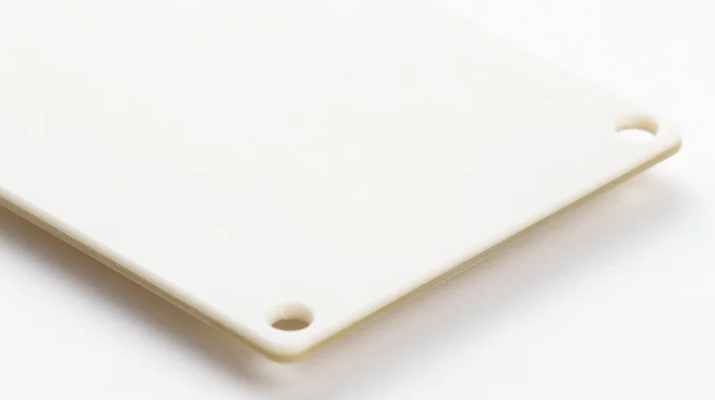
Material Science: The Search for Low-Interference Substrates
In the evolution of high-Tesla diagnostic imaging, the substrate material is no longer just a mechanical support; it is a critical component of electromagnetic signal integrity. Traditional glass-epoxy (FR-4) substrates often contain trace impurities or additives that can induce localized magnetic susceptibility, resulting in image artifacts. Modern engineering focuses on synthetic dielectrics that offer low dielectric constants (Dk) and dissipation factors (Df) while remaining entirely non-ferrous, ensuring that the board geometry does not distort the imaging field.
Comparative Analysis: Ceramic-Filled vs. Specialized Resin Systems
| Feature | Ceramic-Filled Substrates | Advanced Non-Magnetic Resins |
|---|---|---|
| Thermal Stability | High (Low CTE) | Moderate |
| Dielectric Consistency | Excellent at High GHz | High Stability |
| Magnetic Susceptibility | Near-Zero | Inert/Non-Reactive |
| Application Focus | Signal Path Precision | Complex Multilayer Integration |
Ceramic-filled substrates utilize particulate reinforcements to achieve a stable dielectric constant, which is essential for preserving high-frequency waveform phase coherence within the scanner. In contrast, specialized resin systems—such as advanced polytetrafluoroethylene (PTFE) blends—are engineered for mechanical flexibility and optimized loss tangents. While ceramic composites dominate in rigid, high-precision signal routing, specialized resin matrices are increasingly preferred for flexible diagnostic sensor arrays where mechanical fatigue resistance is as vital as signal purity.
Frequently Asked Questions on Substrate Selection
- Why is the Dissipation Factor (Df) important in MRI imaging?
A low Df minimizes signal attenuation and heating, ensuring that high-speed diagnostic data pulses remain clear and free of thermal-induced distortions. - Are ceramic-filled boards compatible with standard manufacturing processes?
While they provide superior stability, ceramic-filled substrates often require specific laser drilling parameters and chemical etching treatments compared to standard resins to ensure reliable via integrity. - Does the substrate material affect the magnetic resonance frequency?
While the substrate does not shift the fundamental Larmor frequency, any magnetic permeability (μr > 1) in the material will perturb the homogeneity of the static magnetic field, directly causing spatial encoding errors.
Component Sourcing and Assembly Constraints
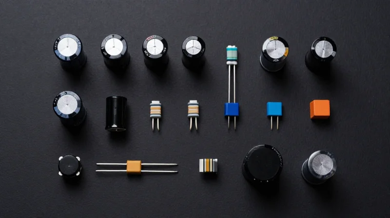
Sourcing Non-Magnetic Bill of Materials
The primary challenge in non-magnetic PCB assembly is the inadvertent introduction of ferrous materials within standard industrial components. Many surface-mount devices (SMDs), particularly resistors and multi-layer ceramic capacitors (MLCCs), utilize nickel-barrier terminations that exhibit significant magnetic susceptibility. Sourcing high-fidelity components requires strict adherence to manufacturer specifications that guarantee non-magnetic materials, such as copper or silver-palladium terminations, rather than nickel.
| Component Type | Magnetic Risk | Non-Magnetic Alternative |
|---|---|---|
| MLCCs | Nickel-barrier plating | Silver/Palladium terminations |
| Resistors | Ferrous metal caps | Non-magnetic film/alloy |
| Connectors | Steel hardware/pins | Brass/Phosphor bronze |
Assembly Constraints and Contamination Control
Assembly environments must be strictly controlled to prevent cross-contamination from standard production lines. Ferrous dust generated by mechanical cutting or drilling processes can settle on boards, causing localized distortions in MRI imaging. Furthermore, the selection of solder alloys and fluxes must prioritize non-magnetic performance, ensuring that no trace elements like iron or cobalt are introduced during the reflow process.
- How do I verify non-magnetic component compliance?
Request a Certificate of Compliance (CoC) and a full material declaration (e.g., IPC-1752A) specifically identifying the absence of ferromagnetic plating layers. - What are the risks of using standard FR-4 assembly lines?
Standard lines often process carbon steel or nickel-plated parts; residual metallic dust or shared handling jigs can lead to microscopic ferrous contamination on sensitive imaging components. - Does hardware selection impact MRI artifacting?
Yes, standard stainless steel screws, standoffs, and fasteners are frequently magnetic. Only 300-series non-magnetic stainless steel or specialized brass hardware should be utilized.
Managing Thermal and Signal Integrity Challenges
The removal of traditional ferrous materials from PCBs often necessitates fundamental shifts in design strategy. Because non-magnetic alloys typically exhibit different thermal conductivities and higher electrical resistances than standard components, engineers must employ advanced layout techniques to prevent localized heat accumulation and maintain signal path fidelity.
Optimizing Thermal Dissipation in Non-Magnetic Environments
In the absence of traditional magnetic heatsinking or steel-based structural supports, thermal management must rely on passive copper-heavy designs and high-thermal-conductivity substrates. Utilizing thickened copper planes (up to 3oz or more) provides the necessary heat spreading without introducing ferrous impurities that would distort magnetic resonance fields.
| Strategy | Thermal Benefit | Signal Integrity Impact |
|---|---|---|
| Thick Copper Planes | High lateral heat distribution | Reduced DC resistance |
| Ceramic Substrates | Superior thermal conductivity | Low dielectric loss at high frequencies |
| Non-Magnetic Thermal Vias | Direct vertical heat transfer | Minimized impedance discontinuities |
Maintaining Signal Integrity (SI) and EMI Shielding
Maintaining signal integrity without steel-based shielding requires a transition to precise board-level layout techniques, including tightly coupled differential signaling and the strategic use of guard traces. Electromagnetic interference (EMI) mitigation must rely on geometric isolation and high-conductivity non-ferrous housings rather than traditional magnetic shielding enclosures.
- How do you handle EMI without standard magnetic shielding?
Engineers utilize selective copper layering, non-magnetic conductive gaskets, and optimized return paths to create effective Faraday cages that are completely transparent to MRI magnetic fields. - What is the primary risk of non-magnetic component substitution?
The primary risk is a change in the coefficient of thermal expansion (CTE) and increased resistive heating, which can lead to premature component failure or signal drift if the layout is not adjusted for the new material properties. - Can standard vias be used in these designs?
Yes, provided the plating chemistry is strictly controlled to exclude nickel or other ferrous materials that are commonly used in standard electroless nickel immersion gold (ENIG) processes.
Testing and Validation for Clinical Compliance
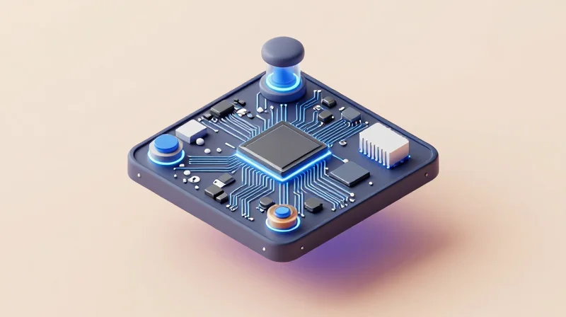
Simulating PCB Performance in High-Field MRI
Before physical prototyping, rigorous electromagnetic (EM) simulation is essential to predict how a PCB assembly will behave within the static and gradient magnetic fields of an MRI scanner. Engineers must perform multi-physics simulations to analyze potential Lorentz forces, induced eddy currents, and RF-induced heating. By utilizing specialized 3D EM simulation tools, developers can map potential signal distortion or image artifacts before committing to manufacturing, significantly reducing the risk of clinical failure.
Benchmarking Validation Protocols
| Test Metric | Traditional PCB | Non-Magnetic Solution |
|---|---|---|
| Ferromagnetic Signature | High risk of mechanical pull | Negligible/None |
| RF Heating Factor | Requires heavy shielding | Optimized for low dissipation |
| Signal Artifacts | Frequent presence of distortion | Clean data acquisition |
Standardized Clinical Compliance Testing
Compliance is governed by international standards, primarily IEC 60601-2-33, which dictates the safety requirements for magnetic resonance equipment for medical diagnosis. Validation testing must include 'in-bore' testing where the PCB is subjected to active gradient pulses to measure signal integrity under real-world clinical conditions. Furthermore, RF-induced temperature rise tests are non-negotiable; assemblies must not exceed prescribed thermal thresholds that could jeopardize patient safety during extended imaging sequences.
Frequently Asked Questions
- How do we verify if a PCB is truly 'non-magnetic'?
Testing should involve both magnetic susceptibility testing using a high-precision SQUID (Superconducting Quantum Interference Device) magnetometer and physical testing with a calibrated force-gauge to detect any residual attraction to a 3T or 7T MRI bore. - Is computational simulation sufficient for regulatory approval?
While essential for design optimization, simulation must be supplemented by empirical data from bench-top testing and standardized phantoms, as defined by FDA and IEC regulatory guidelines. - Why do non-magnetic PCBs require special assembly validation?
Because standard assembly tools, such as tweezers or soldering fixtures, often contain ferrous elements that can induce trace magnetization in sensitive components, specialized non-ferrous manufacturing cleanrooms are often required.
Future-Proofing Medical Devices: A Strategic Approach
Designing for Adaptive Longevity
To future-proof medical devices, engineers must move away from rigid, monolithic board designs. By adopting modular architectural frameworks, manufacturers can isolate non-magnetic components from digital control modules, allowing for rapid hardware upgrades without requiring a complete system redesign. This decoupling strategy ensures that as magnetic flux density requirements evolve, the core signal processing infrastructure remains stable while peripheral imaging front-ends are swapped for modern, compliant iterations.
Strategic Comparison: Static vs. Modular Design
| Design Factor | Traditional Static PCB | Modular Non-Magnetic PCB |
|---|---|---|
| Upgrade Path | Complete system replacement | Component-level replacement |
| Field Compatibility | Fixed threshold (e.g., 1.5T) | Tunable/Upgradable |
| Development Lead Time | Long, complex validation cycles | Rapid, isolated validation |
Key Considerations for Future Readiness
- How do I ensure future compatibility with higher field strengths?
Prioritize the use of non-ferrous, high-purity substrates and silicon-based passives that demonstrate minimal susceptibility signatures, which remains constant even as MRI magnet strength increases. - What role does firmware play in future-proofing?
Firmware abstraction layers allow your hardware to interface with evolving software processing pipelines, enabling performance improvements without physical hardware intervention. - Is modularity cost-effective in the long term?
While modular design increases initial PCB assembly complexity, it drastically lowers the total cost of ownership over a 10-year device lifecycle by eliminating the need for full system recalls during clinical standard updates.
Finally, integrating a 'Digital Twin' validation process during the initial design phase allows engineers to simulate PCB performance under varying magnetic field conditions. This predictive modeling serves as the backbone for certifying new iterations, effectively reducing the time-to-market for the next generation of diagnostic imaging solutions.
Transitioning to non-magnetic PCB technology is no longer optional for those aiming to lead in the high-field diagnostic imaging market. By prioritizing material compatibility and signal purity now, you can avoid costly redesigns and ensure your devices meet the rigorous demands of clinical environments. Contact our engineering team today to audit your current PCB designs or to receive a consultation on our specialized non-magnetic manufacturing capabilities.
