
The shift toward artificial intelligence at the edge is no longer a futuristic concept; it is the current demand of modern smart factories. As devices shrink in size while their computational requirements explode, traditional PCB architectures are hitting their physical and signal integrity limits. This article explores why the transition to High-Density Interconnect (HDI) technology is the defining standard for next-generation industrial reliability.
The Evolution of PCB Requirements in Industrial Edge Computing
From Legacy Constraints to High-Density Demands
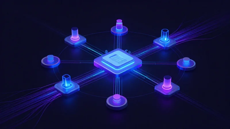
Industrial edge computing is moving beyond simple data collection, now acting as the processing hub for complex AI inferencing and time-sensitive industrial automation. Traditional PCB architectures, characterized by larger component footprints and standard trace routing, are increasingly insufficient for the high-speed signaling and miniaturization requirements of modern edge devices. As component density increases to accommodate powerful SoCs and high-bandwidth memory, engineers are shifting toward High-Density Interconnect (HDI) PCBs to bridge the gap between processing power and form-factor limitations.
Architectural Evolution Comparison
| Requirement | Standard PCBs | Rigid-Flex | HDI PCBs |
|---|---|---|---|
| Signal Integrity | Moderate | High | Very High |
| Component Density | Low | Medium | Ultra-High |
| Thermal Management | Excellent | Challenging | Optimized |
| Manufacturing Cost | Low | Very High | Moderate-High |
Addressing the Modern Engineering Gap
- Why is standard board architecture failing in edge environments?
Standard architectures lack the micro-via capability and layer counts required to manage the high pin-density of modern processors, leading to signal interference and excessive PCB size. - Does rigid-flex offer a better path than HDI?
Rigid-flex is superior for space-constrained mechanical form factors but introduces complexity and cost that often exceed the needs of static edge enclosures where HDI's structural integrity is more reliable. - What is the primary driver for HDI adoption?
The primary driver is the need to shrink trace pitch and via size to accommodate smaller components, which directly reduces signal path lengths and minimizes parasitic effects during high-speed data transmission.
Anatomy of HDI: Why Microvias and Fine Pitch Matter
The Mechanics of HDI: Microvias as the Enabler
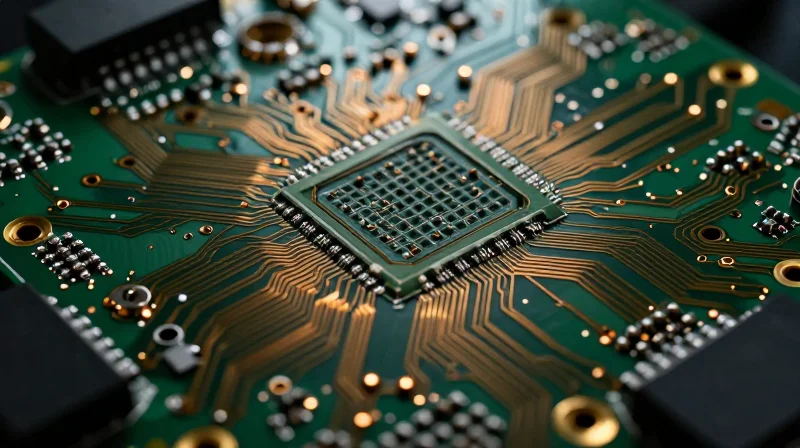
At the heart of the HDI evolution is the shift from through-hole vias to microvias. Traditional PCBs rely on mechanical drills that create large holes passing through multiple layers, consuming significant routing space and forcing larger trace separation. Microvias, conversely, are laser-drilled, blind, or buried structures that connect adjacent layers with diameters typically under 150 micrometers. This physical reduction allows designers to reclaim precious surface area and interior board volume, effectively densifying the signal path without sacrificing performance.
Routing Density Comparison
| Feature | Standard PCB | HDI PCB |
|---|---|---|
| Via Type | Mechanical Through-Hole | Laser-Drilled Microvia |
| Via Diameter | 0.2mm - 0.5mm | <0.15mm |
| Routing Pitch | Coarse (>0.5mm) | Fine (<0.35mm) |
| Layer Utilization | Limited by Drill Size | High via-in-pad density |
The Impact of Fine Pitch Components
The emergence of high-performance SoCs and FPGAs with fine-pitch Ball Grid Array (BGA) packages demands a substrate capable of matching their connectivity requirements. Fine-pitch components feature pads spaced tightly together, often requiring via-in-pad technology to extract signals efficiently. HDI allows for shorter signal paths, which significantly minimizes inductive noise and electromagnetic interference—critical factors when operating high-speed digital signals at the edge.
Common Questions on HDI Architectures
- Why is via-in-pad essential for HDI?
It allows the via to be placed directly within the footprint of a component pad, eliminating the need for dog-bone fan-outs and reducing signal latency. - How do microvias affect signal integrity?
By shortening the signal path and reducing the size of the transition stub, microvias minimize parasitic capacitance and inductance, providing cleaner high-frequency signal transmission. - Does HDI increase the thermal load?
While HDI boards are denser, the increased copper density and improved thermal via placement can actually provide superior heat dissipation pathways from heat-generating components to internal ground planes.
Comparative Analysis: HDI vs. Standard Rigid PCB Architectures
Performance Divergence: HDI vs. Conventional Rigid Boards
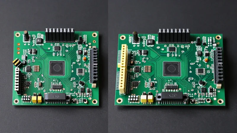
The fundamental difference between HDI and standard rigid architectures lies in the manufacturing methodology regarding interconnection density. Standard rigid PCBs rely on traditional through-hole vias that occupy significant surface area and internal layers, often creating electrical stubs that degrade signal integrity at high frequencies. In contrast, HDI technology leverages microvias and blind/buried via configurations, which drastically shrink the board footprint while simultaneously improving signal propagation by reducing path lengths.
| Feature | Standard Rigid PCB | HDI PCB |
|---|---|---|
| Via Structure | Through-hole | Microvias (Laser-drilled) |
| Routing Density | Low to Moderate | High |
| Signal Integrity | Susceptible to stub effects | Enhanced, lower parasitics |
| Thermal Management | Broad heat dissipation | High localized thermal density |
Trade-offs in Thermal Management and Signal Integrity
While HDI offers clear advantages in space savings, it introduces complex thermal management challenges. By packing components closer together, heat flux density increases, necessitating advanced copper pour techniques and thermal vias to prevent localized overheating. From a signal integrity perspective, HDI is objectively superior for edge computing applications; the ability to use shorter, thinner traces minimizes capacitance and inductance, providing the bandwidth stability required for real-time AI processing.
Comparative FAQs
- Why does HDI outperform standard boards in high-speed applications?
The use of microvias removes parasitic elements like long via stubs, which act as antennas at higher clock speeds, thereby significantly reducing EMI and signal distortion. - Is thermal dissipation more difficult to manage in HDI designs?
Yes, because the higher density of components results in higher power density, requiring more sophisticated thermal simulation and optimized stack-up designs. - When is a standard rigid board still preferable?
For simple, low-density circuitry where space is not a premium and cost-effectiveness via traditional assembly methods is the primary design driver.
When Rigid-Flex Fall Short: Overcoming Complexity Hurdles
The Mechanical and Electrical Bottlenecks of Rigid-Flex
Rigid-flex circuits excel in applications requiring dynamic movement or specific 3D geometry; however, they become a liability when scaled for dense, high-speed edge computing. The transition zones between rigid and flexible layers are notorious weak points for both mechanical failure due to thermal expansion (CTE) mismatches and electrical signal discontinuity. In modern AI applications, where impedance control is paramount, the inability of standard flexible polyimide materials to support high-frequency signal integrity makes rigid-flex increasingly obsolete compared to high-density interconnect (HDI) solutions.
| Constraint | Rigid-Flex Performance | HDI PCB Performance |
|---|---|---|
| Signal Integrity | Variable across transitions | Uniform/High performance |
| Component Density | Moderate/Limited by layers | Extreme/Micro-via enabled |
| Reliability | Prone to flex-zone fatigue | Robust integrated structure |
| Cost at Scale | High (labor-intensive) | Efficient (automated) |
Common Hurdles in High-Speed Applications
- Why does signal integrity drop in rigid-flex?
The transition from the rigid board to the flexible polyimide layer causes variations in the dielectric constant (Dk), which complicates impedance matching and leads to signal reflections in high-speed (25Gbps+) data paths. - How does thermal management differ?
Rigid-flex assemblies often struggle with thermal dissipation because polyimide has lower thermal conductivity than the epoxy-based FR-4 or high-Tg materials used in advanced HDI boards, leading to potential hot spots near high-performance AI processors. - Is rigid-flex still relevant for edge AI?
Only in specific ultra-compact, portable consumer devices where physical bending is a requirement; for stationary or rack-mount industrial edge AI, the added cost and reliability risks of rigid-flex outweigh its spatial benefits.
Transitioning to HDI Architectures
To overcome these hurdles, developers are migrating toward HDI architectures utilizing Any-Layer via technology. By eliminating the reliance on flex-zones and focusing on laser-drilled microvias, engineers can achieve higher routing densities within a rigid, thermally stable substrate. This shift not only simplifies the assembly process but also ensures the consistent electrical pathways necessary for the next generation of AI-driven edge infrastructure.
Signal Integrity and Thermal Management in Compact Spaces

Signal Integrity in High-Density Environments
As board density increases, the proximity of high-speed traces elevates the risk of electromagnetic interference (EMI) and crosstalk. In HDI designs, the use of microvias reduces parasitic inductance compared to traditional through-hole vias, offering superior impedance control for high-speed differential pairs. To maintain signal integrity, engineers must prioritize controlled-impedance routing, utilize buried and blind vias to shorten signal paths, and implement rigorous ground plane referencing to minimize return path discontinuities.
Advanced Thermal Management Strategies
Compact edge computing units often house high-TDP processors that generate intense heat within a constrained volume. Standard cooling solutions are frequently insufficient; therefore, designers must employ thermal vias, copper coins, and specialized thermally conductive prepregs to pull heat away from active components. When comparing architectures, the integration of heat spreaders and heat pipes directly into the PCB stack-up becomes a critical design requirement to avoid localized thermal hotspots.
| Parameter | Standard Boards | HDI PCBs |
|---|---|---|
| Signal Path Length | Long (Inductive) | Short (Optimized) |
| Heat Dissipation | Low (Standard) | High (Thermal Vias/Coins) |
| Crosstalk Risk | Moderate | Low (Better Referencing) |
Frequently Asked Questions
- How do microvias improve thermal performance?
Microvias offer a more direct path through the substrate, allowing for denser thermal via arrays that act as vertical chimneys to transport heat from the top layer to the internal copper planes. - Why is impedance matching harder in compact boards?
Increased routing density forces traces closer together, increasing capacitive coupling and making it difficult to maintain consistent trace widths and spacing, which are essential for stable impedance. - What role does substrate material play in HDI thermal management?
High-glass-transition temperature (Tg) materials are essential for HDI, as they prevent delamination under the extreme thermal cycles common in dense, high-speed edge devices.
Cost-Benefit Analysis for Industrial Hardware Manufacturers
The Economic Trade-off of HDI Integration
While HDI PCBs carry a higher upfront cost due to laser microvias, sequential lamination processes, and high-density material requirements, they represent a strategic investment. The primary value proposition lies in the reduction of board layer counts and total footprint, which can lead to cascading cost savings across the entire assembly, including smaller enclosures, lighter components, and reduced logistics expenses.
| Financial Metric | Standard Rigid PCB | HDI Technology |
|---|---|---|
| Prototyping Cost | Low | High |
| Manufacturing Complexity | Low | High |
| System Enclosure Costs | Moderate | Low (Miniaturization) |
| Field Failure Rates | Moderate | Low (High Reliability) |
Maximizing Lifecycle ROI
Industrial hardware manufacturers must look beyond unit price to realize the true financial impact of board selection. By leveraging HDI, engineers can consolidate multiple legacy boards into a single high-density architecture, significantly simplifying the Bill of Materials (BOM) and reducing assembly labor costs.
- Does HDI improve product longevity?
Yes, by reducing the number of connectors and inter-board cables required, HDI minimizes potential points of failure, directly translating to lower warranty costs and longer field service life. - How does HDI impact speed-to-market?
While initial design time may increase due to complex routing, the streamlined final product architecture allows for faster assembly and integration in subsequent generations. - Is HDI viable for lower-margin hardware?
HDI is often cost-prohibitive for commodity hardware but provides essential competitive differentiation for high-performance edge computing modules where size and thermal efficiency are critical selling points.
Manufacturing Reliability and Long-term Field Performance
Structural Integrity and Field Longevity
The transition to High-Density Interconnect (HDI) technology fundamentally enhances the physical robustness of industrial hardware by minimizing the reliance on mechanical flex zones and complex multi-part assemblies. Unlike traditional rigid-flex PCBs, which are often prone to mechanical failure at the hinge interfaces after thousands of thermal cycles, HDI architectures utilize monolithic board structures that distribute structural stress more uniformly across the substrate.
Reliability Comparison: HDI vs. Traditional Architectures
| Feature | Standard Multi-layer | Rigid-Flex | HDI PCB |
|---|---|---|---|
| Mechanical Fatigue | Low | High (at flex) | Very Low |
| Thermal Expansion Uniformity | Moderate | Low | High |
| Vibration Resistance | High | Moderate | Exceptional |
| Long-term Field Life | 5-7 Years | 3-5 Years | 8-10+ Years |
Environmental Resilience and Thermal Management
HDI boards leverage microvia technology and laser-drilled interconnects that significantly reduce the Coefficient of Thermal Expansion (CTE) mismatch between dielectric materials and copper layers. In industrial environments characterized by rapid temperature fluctuations, this reduction in internal strain prevents common failure modes such as via cracking or pad cratering, ensuring consistent signal path reliability over the product's entire operational lifecycle.
Common Reliability Queries
- How do microvias perform under high-vibration conditions?
Microvias offer higher mechanical strength than through-hole vias due to their reduced size and the increased surface area for solder bonding, providing better resistance to mechanical shear forces in heavy-duty machinery. - Does HDI technology simplify the thermal maintenance of edge devices?
Yes, by allowing for more efficient heat-spreading via buried and blind via structures, HDI reduces localized hot spots that typically accelerate component degradation in standard board layouts. - Are HDI boards more susceptible to moisture ingress?
No; because HDI designs are typically more compact and often fully encapsulated in protective conformal coatings, the reduction in total surface area and complexity inherently lowers the risk of environmental contamination.
Future-Proofing Your Edge Hardware Strategy
The Strategic Mandate for High-Density Interconnects
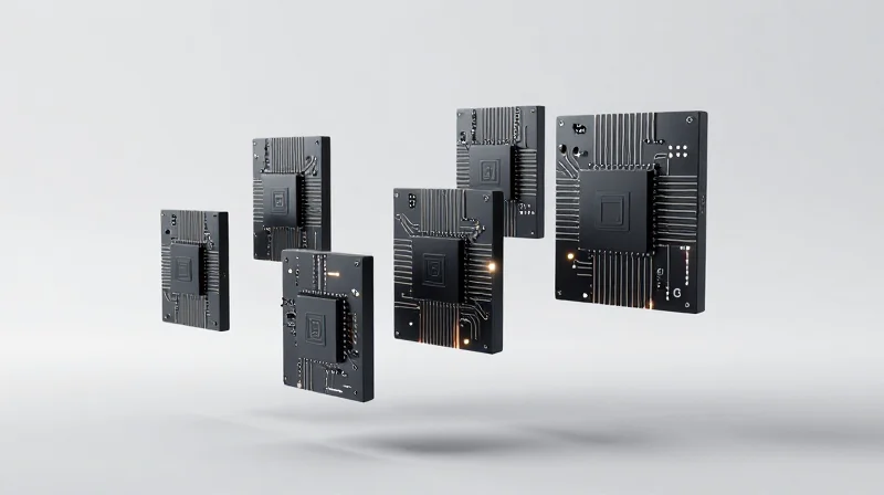
As IoT and edge AI applications demand greater processing power within smaller footprints, standard board architectures are hitting their physical and electrical limits. Moving toward an HDI-centric strategy is no longer optional for firms targeting the next generation of industrial edge devices; it is a prerequisite for maintaining competitive signal density and power efficiency.
| Architecture | Scaling Capability | Best Use Case |
|---|---|---|
| Standard PCB | Low | Basic connectivity sensors |
| Rigid-Flex | Medium | Space-constrained form factors |
| HDI PCB | High | Edge AI & high-speed compute |
Key Considerations for Future-Ready Design
- How do I balance component miniaturization with thermal dissipation?
Utilize thermal via arrays and advanced substrate materials that provide higher thermal conductivity alongside the fine-pitch routing allowed by HDI. - Is HDI cost-prohibitive for mass-market IoT?
While unit costs are higher, the reduction in total layer count and PCB size often offsets expenses through optimized housing dimensions and reduced total system BOM weight. - When should I transition from rigid-flex to HDI?
Transition when the complexity of signal routing for high-speed AI processors exceeds the mechanical advantages of flexible interconnects.
To remain agile, design teams must adopt modular hardware libraries that support HDI manufacturing standards. This allows for rapid iteration and ensures that when components shrink, your manufacturing process is already qualified to support the necessary micro-via structures and pad configurations.
As industrial hardware continues to shrink, the choice of PCB architecture becomes a decisive factor in product performance and longevity. While traditional designs remain relevant for legacy systems, HDI technology provides the bandwidth and density required for modern AI processing. Is your current design roadmap prepared for the next wave of industrial automation? Contact our engineering team today to review your board specifications and ensure your hardware is built for the future.
