
As the demand for hyper-connected industrial IoT and edge computing surges, the humble PCB has become the bottleneck of performance. Moving from standard designs to complex 10-32 layer architectures is no longer just an option—it is a necessity for maintaining signal integrity and power density. This guide explores the technological evolution defining the next generation of electronics packaging.
The Evolution of Multilayer PCB Complexity
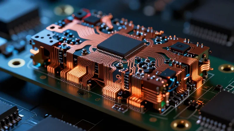
The shift toward high-layer count printed circuit boards (PCBs) is not merely an incremental upgrade but a fundamental transformation necessitated by the density requirements of modern silicon. As integrated circuits grow smaller and more functional, the interconnect density required to support these components has forced engineers to move beyond traditional rigid designs into complex, multi-layered architectures that integrate advanced material science and micro-via technologies.
Drivers of Multilayer Proliferation
- Signal Integrity
As clock speeds increase into the gigahertz range, additional layers are required to manage impedance control and provide dedicated ground planes that mitigate electromagnetic interference. - Component Density
The transition to fine-pitch Ball Grid Array (BGA) components necessitates complex escape routing that cannot be achieved within a two or four-layer footprint. - Power Management
Modern power delivery networks (PDNs) require multiple voltage rails and high-current paths, effectively consuming board real estate that necessitates deeper layering to maintain thermal stability.
Technological Milestones in PCB Fabrication
| Development Era | Primary Technology | Complexity Focus |
|---|---|---|
| 1990s-2000s | Through-hole PTH | Increased surface area |
| 2010s | HDI (High-Density Interconnect) | Micro-via implementation |
| 2020s-Present | Any-Layer/ELIC | Vertical interconnect density |
The evolution has culminated in 'Any-Layer' technology, also known as Every Layer Interconnect (ELIC). This method allows for vertical stacking of micro-vias between any two layers of the PCB, effectively removing the constraints of traditional buried and blind via structures. This shift allows for unprecedented routing density, essentially turning the board into a three-dimensional lattice capable of supporting the most advanced system-on-chip architectures in use today.
Critical Challenges in High-Layer Count Manufacturing
Precision Registration and Interconnect Integrity
As layer counts scale toward 32 and beyond, the tolerance for physical deviation shrinks exponentially. The primary challenge lies in maintaining precise registration across an increasingly thick laminate stack. During lamination, thermal expansion and mechanical stress can cause localized shifts, leading to interconnect misalignment between microvias and inner-layer pads. Achieving sub-micron alignment requires sophisticated LDI (Laser Direct Imaging) systems combined with advanced compensation algorithms that predict material deformation patterns based on copper density distribution.
Thermal Management and Z-Axis Stability
High-layer count boards act as heat reservoirs. The mismatch between the Coefficient of Thermal Expansion (CTE) of dielectric materials and copper leads to severe Z-axis expansion during thermal cycling or soldering operations. This expansion often results in barrel cracking of through-hole vias or delamination at the interface of internal layers. Designers must utilize high-Tg (glass transition temperature) materials to maintain structural integrity under persistent thermal stress.
| Challenge Type | Technical Driver | Impact on Reliability |
|---|---|---|
| Registration | Material Lamination Stress | Open circuits/Misaligned vias |
| Thermal Management | CTE Mismatch | Barrel cracking/Delamination |
| Signal Integrity | Via Stub Effects | Data loss/EMI issues |
Frequently Asked Questions on High-Layer Fabrication
- How does aspect ratio impact drilling for 32+ layer boards?
Higher aspect ratios make laser and mechanical drilling significantly more difficult, increasing the risk of incomplete copper plating within deep vias and potential signal degradation. - Why is surface finish flatness critical for high-layer counts?
For fine-pitch BGA components often used on these dense boards, any non-planarity in the surface finish can lead to bridging during reflow or poor solder joint formation. - Is moisture absorption a concern for reliability?
Yes, high-layer boards are more susceptible to internal moisture entrapment, which can cause 'popcorning' during high-temperature assembly processes if moisture content is not strictly controlled.
Next-Generation Interconnect Technologies: Beyond Traditional Vias
Moving Beyond Conventional Via Architectures
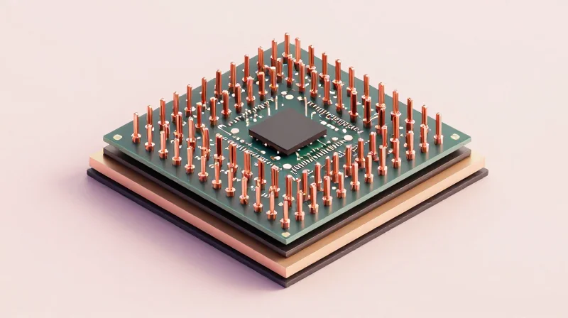
As layer counts climb, traditional mechanical drilling reaches physical limits, necessitating a shift toward sophisticated interconnect strategies. Any-layer high-density interconnect (HDI) technology—frequently referred to as Any-Layer Via (ALIVH)—allows for copper-filled, stacked microvias between any two layers. This transition eliminates the reliance on bulky through-holes that occupy valuable routing space and introduce unwanted parasitic capacitance.
| Technology | Routing Density | Signal Integrity Impact | Primary Application |
|---|---|---|---|
| Standard Thru-Hole | Low | High Inductance | Backplane/Legacy |
| Blind/Buried Vias | Moderate | Improved | High-Speed Computing |
| Any-Layer HDI | Ultra-High | Minimal Parasitics | Mobile/AI Accelerators |
The Role of Laser Microvias and Copper Filling
Laser direct ablation has become the cornerstone of modern miniaturization, enabling the formation of microvias with aspect ratios that mechanical drills cannot achieve. Subsequent copper-filled plating processes are essential to ensure the reliability of these stacked via structures, providing the thermal conductivity and mechanical integrity required to handle high-density ball grid array (BGA) pitches.
Frequently Asked Questions on Interconnect Shifts
- Why is Any-Layer technology superior for high-layer counts?
It allows for unlimited routing freedom, enabling signal traces to jump between any two adjacent layers without traversing the entire thickness of the board, which drastically reduces signal crosstalk. - What is the primary reliability concern with stacked microvias?
The main concern is thermal expansion mismatch (CTE) between the copper fill and the surrounding dielectric. Modern conductive pastes and advanced plating chemistries are employed to mitigate micro-cracking. - Does switching to laser-drilled microvias increase manufacturing time?
Yes, laser processes are sequential. While they offer superior density, the cycle time per layer increases compared to traditional drilling, necessitating a trade-off between board performance and throughput efficiency.
Mastering Signal Integrity at High Speeds

As layer counts climb, maintaining signal integrity (SI) shifts from a routine task to a critical engineering discipline. The reduction in track width and spacing necessitated by high-density interconnect (HDI) requirements elevates the risk of capacitive coupling, inductive noise, and reflections. Engineers must now account for glass-weave effects, dielectric constant (Dk) stability, and surface roughness to preserve signal fidelity at speeds exceeding 56Gbps PAM4.
Mitigating Signal Degradation Mechanisms
To achieve operational reliability, designers must implement rigorous strategies against three primary threats: crosstalk, impedance variance, and attenuation.
| Challenge | Primary Mitigation Strategy | Technical Focus |
|---|---|---|
| Crosstalk | Differential Impedance Control | Increase gap-to-height ratio and utilize field-stitching vias. |
| Impedance Mismatch | Back-drilling & Impedance Matching | Eliminate via stubs and tune trace geometry to match dielectric properties. |
| Signal Attenuation | Low-Loss Dielectric Materials | Minimize dissipation factor (Df) and optimize copper foil profile. |
Advanced Mitigation Tactics
- How do we counteract glass-weave effects?
Utilize spread-glass or mechanically flattened weave patterns to ensure a uniform dielectric constant under high-speed traces, preventing skew caused by differing propagation speeds. - Why is back-drilling critical for high-layer counts?
Back-drilling removes unused portions of plated through-holes (stubs). At frequencies above 10GHz, these stubs act as resonant antennas, severely degrading the signal and creating unacceptable reflection nodes. - What role does surface roughness play?
At high frequencies, the skin effect concentrates electron flow near the copper surface. Using low-profile or 'VLP' (Very Low Profile) copper reduces parasitic inductance and insertion loss.
Successful SI management in complex multilayer structures ultimately depends on early-stage simulation and co-design. Utilizing 3D full-wave electromagnetic solvers alongside pre-layout SI analysis allows for the identification of potential EMI hotspots before the manufacturing cycle begins, saving critical time in the development of modern electronics.
Advanced Materials and Substrate Selection
The Shift Toward Ultra-Low Dk and Df Materials
As data rates reach 112Gbps and beyond, the dielectric properties of PCB substrates become the primary bottleneck for performance. Traditional FR-4 laminates suffer from excessive signal attenuation and dielectric absorption at these frequencies. Engineers are increasingly moving toward specialized resins—such as polyphenylene ether (PPE) and hydrocarbon-based systems—that offer ultra-low dielectric constant (Dk) and dissipation factor (Df). By minimizing these parameters, designers can achieve lower signal insertion loss, reduce propagation delay, and ensure that high-speed signals maintain their integrity over complex multilayer interconnects.
Material Performance Comparison
| Material Class | Dk (at 10GHz) | Df (at 10GHz) | Primary Application |
|---|---|---|---|
| Standard FR-4 | 4.4 - 4.8 | 0.015 - 0.020 | Low-speed digital |
| High-Tg Mid-Loss | 3.8 - 4.1 | 0.008 - 0.010 | Mainstream server |
| Ultra-Low Loss (PTFE-based) | 2.5 - 3.2 | 0.001 - 0.003 | High-speed networking |
Key Considerations in Substrate Selection
- How does moisture absorption impact performance?
Materials with high moisture absorption rates experience shifts in Dk as ambient humidity changes, which can lead to unpredictable impedance variations in dense boards. - Why is Coefficient of Thermal Expansion (CTE) stability critical?
In high-layer count PCBs, mismatched CTE between copper and substrate causes mechanical stress during thermal cycling, risking via barrel cracking and layer delamination. - What role does copper surface roughness play?
At high frequencies, the 'skin effect' causes signals to travel along the surface of the copper; therefore, ultra-low profile (VLP) copper is essential to reduce resistive losses.
Beyond electrical performance, the manufacturing processability of advanced substrates remains a significant hurdle. Materials like PTFE (Teflon) require specialized surface treatments and plasma etching processes for reliable plating. Future packaging trends point toward the adoption of hybrid constructions—using ultra-low loss materials for high-speed signal layers while utilizing more cost-effective cores for ground and power planes—to balance electrical excellence with economic feasibility.
Thermal Management Strategies for Dense Electronics
Integrated Thermal Dissipation Techniques
As component density increases, traditional surface cooling is no longer sufficient. Modern architectures leverage the PCB itself as a thermal conduit. By incorporating solid copper coins, heavy-copper internal planes, and high-density thermal via arrays, heat is efficiently shunted away from high-power ICs and redistributed across the board's surface area. Advanced metal-core printed circuit boards (MCPCBs) and thermally conductive prepregs are now standard in server-grade designs to bridge the gap between high-power semiconductors and external heat sinks.
Thermal Management Material Comparison
| Technique | Thermal Conductivity | Primary Application |
|---|---|---|
| Copper Coins | Excellent (>350 W/mK) | High-wattage processors |
| Thermal Vias | Moderate (15-25 W/mK) | Localized component cooling |
| Thermally Conductive Prepreg | High (3-5 W/mK) | Multi-layer heat spreading |
| Aluminium Substrate | High (200+ W/mK) | LED and power conversion |
Frequently Asked Questions
- How do thermal vias impact signal integrity?
While thermal vias provide a path for heat, they can create parasitic capacitance and inductance. Careful spacing and decoupling from high-speed traces are essential to prevent signal crosstalk. - When should copper coins be preferred over standard vias?
Copper coins are recommended for components exceeding 50W, where standard plated-through-hole thermal vias cannot provide the necessary cross-sectional area for heat transfer. - Does board thickness affect cooling performance?
Yes; thinner boards with higher copper content per layer often perform better for heat spreading, as they reduce the thermal resistance distance between the heat source and the cooling solution.
Automated Optical Inspection and Quality Control
The Evolution of Inspection in High-Layer Architectures
As layer counts climb beyond 20 layers with increasingly miniaturized features, manual inspection has become obsolete. Modern manufacturing now relies on AI-driven Automated Optical Inspection (AOI) combined with Automated X-Ray Inspection (AXI) to peer into internal layers. These systems utilize machine learning algorithms to distinguish between acceptable design variations and catastrophic manufacturing defects, such as registration shifts, microvia voids, or annular ring violations in ultra-dense HDI designs.
Technological Comparison: AOI vs. AXI
| Feature | AOI (Optical) | AXI (X-Ray) |
|---|---|---|
| Primary Use Case | Surface-level copper features | Internal layers and blind/buried vias |
| Detection Capability | Shorts, opens, cosmetic defects | Misalignment, voiding, BGA solder joints |
| Inspection Speed | High throughput | Slower; typically used for sampling |
Integrating Smart Quality Control
Moving toward Industry 4.0, quality control is transitioning from a reactive end-of-line verification to a real-time, closed-loop feedback system. By correlating AOI data with laser direct imaging (LDI) parameters, manufacturers can adjust etching processes dynamically. This preventative approach minimizes scrap rates in expensive high-layer builds, where even a single layer failure can render a complex board valueless.
- How does AI enhance AOI in high-layer boards?
AI reduces false call rates by learning the unique topography of dense high-layer designs, allowing the system to ignore harmless artifacts while highlighting genuine structural risks. - Why is 100 percent inspection vital for high-layer PCBs?
The inherent complexity of 20+ layer boards makes manual probing impossible; automated inspection ensures that internal defects like microvia cracks are caught before final assembly. - What is the role of Big Data in PCB quality control?
Aggregated inspection data provides trace-back capabilities, allowing manufacturers to identify root-cause material or process drifts before they manifest as systemic defects.
Future Outlook: AI-Driven Design and Fabrication

The Convergence of AI and PCB Design
As multilayer PCBs exceed 30+ layers with increasingly complex blind and buried via structures, manual design methodologies have become a bottleneck. Artificial Intelligence is moving from a novelty to a fundamental requirement in electronics packaging. Machine learning algorithms now facilitate generative design by exploring thousands of placement and routing iterations in seconds, optimizing for signal integrity, power distribution, and thermal performance simultaneously.
AI-Driven Fabrication and Yield Optimization
Beyond design, AI is transforming the factory floor. By integrating real-time data from Automated Optical Inspection (AOI) and X-ray systems, AI-powered systems can predict manufacturing defects before they manifest. This closed-loop feedback mechanism dynamically adjusts lithography parameters and laser drilling intensities to compensate for material registration shifts, significantly enhancing the yield of high-layer count boards.
| Feature | Traditional Methodology | AI-Driven Paradigm |
|---|---|---|
| Routing Complexity | Manual/Heuristic-based | Generative/ML-optimized |
| Defect Detection | Post-process inspection | Predictive/Pre-process correction |
| Design Cycle | Linear/Iterative | Parallel/Rapid Synthesis |
Key Implications for Manufacturers
- How does AI impact time-to-market?
AI automation drastically reduces design cycle times by automating routine routing tasks and validating complex signal constraints at the speed of computation. - Is human intervention still required?
Yes, while AI handles complex optimization, human engineers remain essential for defining high-level architectural intent and verifying compliance with strict industrial standards. - Will AI improve structural reliability?
Absolutely; by optimizing copper distribution and thermal via arrays through predictive modeling, AI creates inherently more stable and reliable board geometries.
As layer counts climb and performance tolerances tighten, staying ahead requires mastery of both materials and manufacturing precision. By adopting these advanced strategies, your team can ensure superior signal integrity and reliability in every design. Ready to elevate your hardware capabilities? Contact our engineering team today to discuss your next high-layer PCB project.
