
In the race toward 224G and beyond, the copper traces on your circuit boards are no longer just wires; they are complex transmission lines. As signal frequencies soar, even minor manufacturing deviations become catastrophic to data integrity. This article explores the shift from standard fabrication methods to the advanced processes required for the next generation of high-speed electronics.
The 112G+ Threshold: Why Traditional Methods Are Failing

The Physics of Failure at 112G and Beyond
At speeds reaching 112Gbps and beyond, copper traces cease to behave as simple DC paths and instead function as complex high-frequency wave-guides. Traditional impedance control techniques—which rely on static geometric approximations—are failing because they do not account for the microscopic impacts of copper surface roughness and the non-linear nature of dielectric dissipation factors. In this regime, even sub-millimeter manufacturing variations cause catastrophic phase jitter and signal eye closure.
Comparative Analysis of Signal Loss Mechanisms
| Loss Mechanism | 10G-25G Impact | 112G+ Impact |
|---|---|---|
| Skin Effect | Manageable | Dominant; requires ultra-low profile copper |
| Dielectric Loss | Secondary concern | Critical; requires low-loss Dk/Df materials |
| Surface Roughness | Negligible | Primary source of insertion loss |
Critical Industry Questions
- Why does copper surface roughness matter more at 112G?
As frequency increases, the skin depth of the signal decreases to the point where the signal current travels within the rough microscopic texture of the copper foil, effectively increasing the path length and resistance. - Can traditional laminate materials support 112G?
Standard FR-4 laminates exhibit too much dielectric absorption at these frequencies, leading to intolerable signal degradation; designers must transition to specialized, ultra-low-loss PTFE or ceramic-filled resin systems.
To maintain signal integrity at 112G, engineers must move away from 'design-for-manufacturing' (DFM) as an afterthought and move toward 'design-for-physics'. This involves 3D electromagnetic modeling of every transition and via, rather than relying on 2D cross-sectional impedance calculations that ignore real-world trace geometry.
The Anatomy of Impedance Control in High-Frequency Boards
The Physical Pillars of Impedance Precision
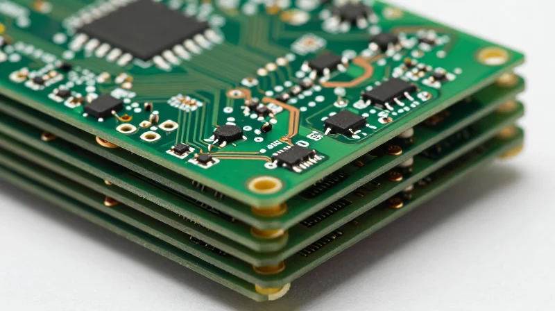
Achieving stable impedance in high-speed circuits requires moving beyond simple trace width calculations. As signal speeds surpass 112G, the micro-topography of the copper conductors and the molecular consistency of the dielectric material become the primary drivers of signal integrity and reflection losses.
Copper Surface Roughness: The Skin Effect Multiplier
At high frequencies, the skin effect confines current to a microscopic layer near the copper surface. If the copper foil possesses a high profile (rough surface), the effective path length of the electrons increases, raising resistive losses and altering the effective inductance. For next-generation electronics, utilizing Very Low Profile (VLP) or Hyper-Low Profile (HVLP) copper is essential to minimize insertion loss and maintain a predictable impedance profile.
Dielectric Uniformity and the Glass Weave Effect
Dielectric constants (Dk) are rarely isotropic in standard FR-4 laminates due to the glass fiber weave. As high-speed signals travel, they experience varying Dk values depending on whether the trace aligns with a glass bundle or an epoxy-rich region. This 'fiber weave effect' creates periodic impedance discontinuities, causing phase skew and jitter. Advanced designs now prioritize spread glass or non-woven substrates to achieve a homogeneous dielectric environment.
| Parameter | Impact on Impedance | High-Speed Requirement |
|---|---|---|
| Copper Roughness | Increases effective inductance/loss | Use HVLP copper foils |
| Dk Uniformity | Causes signal skew/phase shifts | Utilize spread glass weave |
| Etch Factor | Alters trace geometry/shape | Strict controlled-impedance etching |
- Why does copper roughness matter at 112G?
As frequency increases, the skin depth becomes comparable to the surface roughness, causing the signal to follow the irregular topography of the copper, which increases resistance and degrades signal integrity. - How do designers mitigate the fiber weave effect?
Designers employ rotated board layouts (typically at 10-degree angles), specify spread glass fabrics, or transition to higher-end ceramic-filled PTFE substrates for improved dielectric consistency.
Evaluating Legacy Fabrication: Limitations of Etch Factors
As signal frequencies push toward 112G and beyond, the margins for impedance deviation shrink dramatically. Traditional subtractive manufacturing relies on chemical etching, a process fundamentally limited by the 'etch factor'—the ratio of vertical to lateral material removal. Because etchants act isotropically, they inevitably erode the sides of copper traces while eating through the resist, resulting in trapezoidal profiles rather than precise rectangular cross-sections. In modern high-speed designs, this geometric uncertainty introduces significant impedance mismatches that lead to reflections and signal degradation.
The Geometry of Etch Inconsistency
The primary challenge with legacy fabrication is the lack of uniformity across the panel. Etch rates fluctuate based on copper distribution density and chemical flow dynamics, causing variations in trace width and side-wall angle. For high-speed differential pairs, where coupled impedance depends on the tight control of spacing and width, even a 5% deviation in copper cross-section can cause a 5-10 Ohm impedance spike. This is compounded by 'undercutting,' where the etchant removes copper beneath the protective photoresist, further destabilizing the electrical footprint of the trace.
| Parameter | Legacy Etching Impact | High-Speed Consequence |
|---|---|---|
| Trace Profile | Trapezoidal | Increased effective inductance |
| Width Tolerance | ±10% to ±15% | Impedance discontinuity |
| Etch Factor | Variable (Process dependent) | Phase velocity variations |
Common Limitations in Legacy Impedance Control
- Why does the side-wall angle matter?
A non-vertical side-wall changes the effective capacitance between the trace and the reference plane, directly impacting the target impedance calculation. - How does copper grain structure interact with etching?
During chemical etching, preferential attack at grain boundaries increases the effective roughness (Rz), which triggers skin effect losses that are no longer predictable through simple geometry. - Can compensation designs fix etch factors?
While designers use trace width compensation, chemical fluctuations are often too stochastic to account for across large, complex high-density interconnect (HDI) boards.
Moving forward, the industry must transition from legacy chemical subtractive methods to additive manufacturing or advanced semi-additive processes (SAP). These methods offer the verticality and dimensional stability required to maintain signal integrity at the 112G threshold, effectively decoupling geometric precision from the limitations of chemical etch factors.
The Role of Next-Gen Dielectric Materials

The Physics of Dielectric Loss
As signal frequencies climb, the dielectric substrate transitions from a mere physical carrier to an active participant in signal attenuation. The two primary metrics governing this performance are the Dielectric Constant (Dk) and the Dissipation Factor (Df). High-speed designs require materials with low Dk to manage propagation delay and, more critically, low Df to minimize energy absorption by the material, which manifests as insertion loss.
Material Performance Comparison
| Material Class | Typical Dk | Typical Df | Primary Use Case |
|---|---|---|---|
| Standard FR-4 | 4.4 - 4.8 | 0.020 | Low-speed digital |
| Mid-Loss Laminates | 3.6 - 3.9 | 0.008 | Standard networking |
| Ultra-Low Loss PTFE | 2.1 - 2.5 | 0.001 | 112G/224G SerDes |
| Ceramic-Filled Resin | 3.0 - 3.4 | 0.002 | High-frequency RF/Antenna |
Addressing Copper Roughness and Glass Weave Effects
Beyond the bulk dielectric properties, the microscopic interface between copper and substrate significantly impacts signal propagation. Standard copper profiles introduce 'skin effect' losses, where high-frequency signals follow the topography of the foil. Next-gen materials now utilize VLP (Very Low Profile) copper to mitigate this. Furthermore, glass-reinforced laminates suffer from the 'glass weave effect,' where localized Dk variations cause signal skew. Advanced substrates now employ spread-glass or non-woven structures to ensure dielectric uniformity across the board surface.
Frequently Asked Questions
- Why is low-Df critical for 112G systems?
At 112G and beyond, the dielectric absorption loss can exceed conductor loss; a low-Df material minimizes the conversion of signal energy into heat, preserving signal eye-opening. - How does glass weave affect high-speed signals?
Differential pair traces running over a fiber glass bundle versus resin-rich areas experience different phase velocities, causing timing skew and degraded bit-error rates. - Are there trade-offs in choosing ultra-low loss materials?
Yes, high-performance materials often feature higher moisture absorption rates, lower adhesion strength, and significantly higher fabrication costs compared to standard epoxy-based substrates.
Advancements in Laser-Direct Imaging (LDI) Technologies

Overcoming Traditional Photolithography Constraints
Traditional photolithography relies on physical film masks, which are susceptible to thermal expansion, dimensional instability, and alignment errors. In contrast, LDI utilizes high-precision laser beams to directly pattern the resist, eliminating mask-related defects. This shift is critical for high-speed designs where even minor variations in trace width—often caused by mask misalignment or uneven light distribution—can lead to significant impedance discontinuities.
Precision and Impedance Consistency
LDI allows for adaptive scaling, where the system adjusts the exposure geometry on the fly to compensate for substrate distortions. This ensures that trace geometries remain consistent across the entire panel, which is the cornerstone of maintaining controlled impedance in high-bandwidth applications like 112G and 224G SerDes interfaces.
| Feature | Legacy Photolithography | Laser-Direct Imaging (LDI) |
|---|---|---|
| Registration Accuracy | Limited by mask stability | Dynamic, sub-micron precision |
| Trace Geometry | Inconsistent at <2 mil | Uniform sub-mil features |
| Setup Time | High (mask production) | Low (direct digital input) |
| Impedance Variance | Moderate to High | Very Low |
Key Advantages for High-Speed Design
- How does LDI improve signal integrity?
By providing superior resolution and registration, LDI ensures trace widths are exact, minimizing reflections caused by impedance mismatches in high-frequency signals. - Can LDI handle modern ultra-thin substrates?
Yes, LDI's ability to adjust for material distortion makes it ideal for the flexible or ultra-thin cores often found in high-speed, high-density interconnect designs. - Is LDI the standard for future-proofing?
As signal frequencies climb, the margin for error shrinks. LDI is currently the only scalable technology capable of meeting the tight tolerances mandated by the next generation of high-speed standards.
Copper Surface Treatment: Mitigating High-Frequency Loss
The Skin Effect and Surface Roughness Interaction
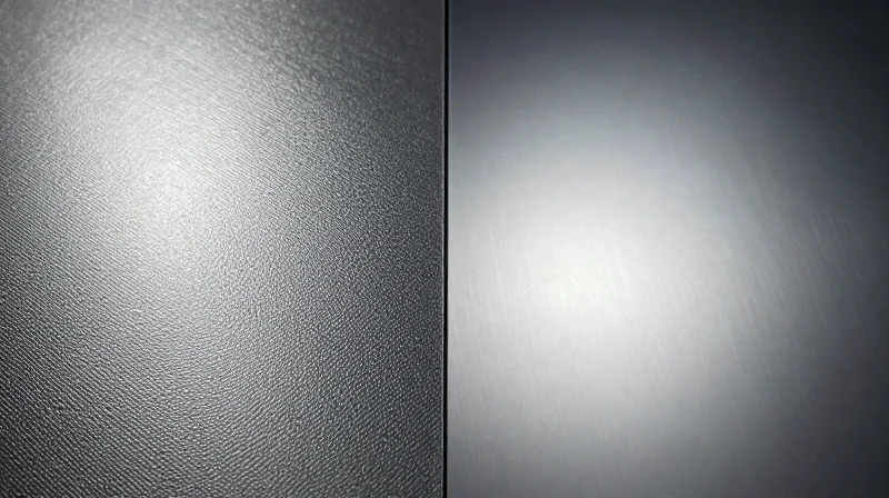
At high frequencies, the skin effect confines current flow to the surface layer of the copper trace. If the copper surface is rough—a common byproduct of traditional bonding treatments—the signal path becomes effectively longer, and the current must navigate a complex, irregular topography. This phenomenon, known as conductor loss, significantly exacerbates insertion loss and signal degradation. By employing ultra-low profile (ULP) or VLP (very-low profile) copper, engineers can drastically reduce these parasitic effects, ensuring cleaner signal propagation at multi-gigabit speeds.
Comparative Analysis of Copper Profiles
| Copper Type | RMS Roughness (Rq) | Signal Integrity Impact | Recommended Application |
|---|---|---|---|
| Standard Electro-deposited | 2.0 - 3.5 µm | High Loss (Skin Effect) | Low-speed / DC power |
| Very Low Profile (VLP) | 1.0 - 1.5 µm | Moderate Loss | Standard high-speed |
| Ultra-Low Profile (ULP) | < 0.5 µm | Minimal Loss | 28Gbps+ / 56Gbps+ |
Surface Treatment Strategies
Beyond copper selection, the chemical treatments used to improve adhesion between the copper and the dielectric laminate play a critical role. Modern fabrication facilities are transitioning toward chemical treatments like organometallic coupling agents instead of mechanical roughening (e.g., pumice scrubbing or traditional chemical etching). These advanced treatments maintain the integrity of the copper surface while providing sufficient bond strength to survive thermal cycling during assembly.
- Why does copper roughness matter at 50GHz?
At high frequencies, the current flows primarily in the outer few microns of the trace; surface irregularities force the current to follow a tortuous path, increasing effective resistance and phase distortion. - Is there a trade-off for using ULP copper?
Yes, ULP copper often presents challenges with laminate adhesion; therefore, high-performance bonding films or proprietary oxide-replacement surface treatments must be implemented to prevent delamination during reflow. - Does surface treatment replace the need for low-loss laminates?
No, surface treatment complements low-loss materials. Even with ultra-low Dk/Df substrates, poor copper surface preparation can nullify the performance gains achieved by the dielectric material.
Strategic Manufacturing: Integrating Design for Manufacturing (DFM) Early
Shifting Paradigms: From Sequential to Collaborative Design
Traditional PCB workflows often treat fabrication as an afterthought, creating a bottleneck where design constraints clash with manufacturing capabilities. In the era of high-speed, high-density interconnects, waiting until the prototype stage to address impedance control is a strategy prone to failure. By integrating DFM principles at the schematic and layout phases, engineers can preemptively align stackup geometries and material selection with the fabrication house's specific tolerances.
Key DFM Strategies for Impedance-Controlled Designs
- Proactive Stackup Collaboration
Engage fabricators during the initial stackup definition to ensure the selected dielectric materials and copper weights align with their controlled impedance processing limits. - Width and Spacing Optimization
Adjust trace geometries based on the specific etching bias of the manufacturer, ensuring target impedance values are maintained within tight tolerance windows. - Material Compatibility Checks
Verify that high-frequency low-Dk/low-Df materials are compatible with the fabricator's standard drilling and plating processes to avoid thermal degradation or signal loss.
Comparison of Design Approaches
| Feature | Sequential Design Approach | Early DFM Integration |
|---|---|---|
| Risk Assessment | Post-layout, high cost of change | Pre-layout, proactive mitigation |
| Impedance Accuracy | Often relies on manufacturer adjustments | Designed to fabricator process capabilities |
| Time-to-Market | Extended by prototype rework | Accelerated through first-pass success |
To implement these practices effectively, designers should leverage automation scripts that pull live process data from the manufacturer directly into the CAD tool. This creates a feedback loop where the design environment automatically flags impedance violations based on current etching capabilities, ensuring that performance specs and manufacturability are synchronized throughout the development lifecycle.
The Path Forward: Future-Proofing Your High-Speed Infrastructure
The Convergence of Material Science and Process Control
As signal frequencies move into the multi-gigabit and terahertz range, the PCB is no longer a passive substrate but an active component of the circuit. Future-proofing necessitates a move away from standard FR-4 towards advanced PTFE or ceramic-filled thermoset laminates that offer stable dielectric constants across a wider frequency spectrum. Simultaneously, these materials must be paired with manufacturing processes like additive metallization to maintain the geometric precision that traditional subtractive etching can no longer guarantee.
| Focus Area | Legacy Approach | Future-Proof Strategy |
|---|---|---|
| Dielectric Choice | Standard FR-4 / Glass | Engineered Low-Loss PTFE/LCP |
| Etching Method | Chemical/Subtractive | Additive/Semi-Additive Process |
| Design Integration | Siloed DFM | Co-Design Modeling |
Strategic Implementation FAQ
- How does early DFM influence future-proofing?
Early DFM allows engineers to account for manufacturing tolerances like copper roughness before the design is finalized, preventing impedance mismatches that emerge only at high frequencies. - Why is surface treatment critical for next-gen designs?
Ultra-low profile (ULP) copper reduces the skin effect impact, where electrons travel through the jagged surface of standard copper, leading to significant signal loss and phase jitter. - What is the role of simulation in modern infrastructure?
Digital twins and full-wave electromagnetic solvers are now mandatory to predict performance across heterogeneous material stacks, effectively bridging the gap between theoretical schematics and physical hardware.
Automating Precision
To achieve long-term scalability, organizations must automate the feedback loop between board houses and design teams. By integrating real-time manufacturing data—such as trace width variations measured by LDI systems—back into the design suite, firms can calibrate their impedance models dynamically. This closed-loop approach transforms manufacturing constraints from static obstacles into adaptive variables, ensuring the integrity of high-speed signals as data rates continue their exponential trajectory.
Navigating the complexities of 112G+ design requires a shift from traditional fabrication to a materials-first methodology. By embracing laser-direct imaging and advanced dielectric solutions, your designs can overcome the physical limits of current technology. Contact our engineering team today to audit your high-speed layout and optimize it for the next generation of data performance.
