
The Industrial Internet of Things (IIoT) is at a critical inflection point. As sensor nodes shrink and demands for high-speed interconnect density surge, traditional manufacturing methodologies are beginning to show their seams. For engineers building the foundation of tomorrow's industrial automation, understanding the shift from legacy PCB designs to high-reliability, next-generation architectures is no longer optional—it is the prerequisite for long-term viability.
The Evolution of Sensor Nodes in Industrial Environments
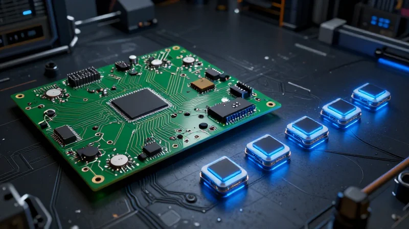
The evolution of sensor nodes within industrial environments represents a shift from basic connectivity to sophisticated, decentralized intelligence. Historically, industrial sensing relied on rigid, single-purpose Printed Circuit Board (PCB) assemblies that prioritized raw data transmission over local processing. As Industrial IoT (IIoT) requirements have matured, these nodes have migrated toward compact, multi-functional units capable of real-time diagnostics and predictive maintenance, driven by the need for higher energy efficiency and enhanced computational capacity.
From Legacy Constraints to Modern Performance
| Feature | Legacy PCB Architectures | Next-Gen Sensor Nodes |
|---|---|---|
| Processing | Centralized (Cloud/PLC) | Edge-based (AI/ML) |
| Form Factor | Large, Enclosure-heavy | Miniaturized, SiP Integrated |
| Connectivity | Wired Industrial Bus | LPWAN, 5G, Mesh |
| Ruggedization | Bulk Protection | Material-science Driven |
Core Drivers of Architectural Change
- Why is edge computing critical for modern sensor nodes?
Edge computing reduces latency and bandwidth overhead by performing data filtering and analysis locally, ensuring only actionable insights are transmitted over the network. - How have physical requirements changed in IIoT?
Modern nodes must occupy minimal space to integrate directly into robotic actuators and rotating machinery, requiring System-in-Package (SiP) technologies rather than traditional bulky PCB layouts. - What role does harsh environment survivability play?
Next-gen architectures prioritize thermal management and vibration resistance at the component level, moving beyond simple external housing to utilize advanced potting compounds and ceramic substrates.
The architectural shift is fundamentally defined by the transition from discrete component integration to Systems-on-Chip (SoC) and high-density interconnect designs. By consolidating power management, sensing, and low-power wireless communication onto smaller board footprints, manufacturers can deploy sensors in previously inaccessible locations, effectively closing the loop in real-time industrial telemetry.
The Limitations of Legacy PCB Methodologies
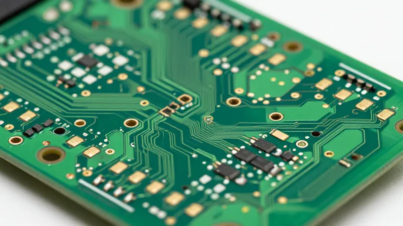
The Inherent Constraints of Traditional PCB Architectures
Legacy PCB design and manufacturing processes were fundamentally optimized for stationary, climate-controlled environments where mechanical robustness and thermal dissipation were secondary to cost-effective volume production. In the context of the Industrial Internet of Things (IIoT), these traditional methodologies fail to account for the radical miniaturization and extreme reliability requirements imposed by intelligent, edge-deployed sensor nodes.
Comparison: Legacy PCB vs. Next-Gen Requirements
| Requirement | Legacy Methodology Limitation | IIoT Operational Reality |
|---|---|---|
| Thermal Management | Reliance on bulky heat sinks | High-density convection-less cooling |
| Mechanical Stress | Rigid substrates susceptible to cracking | High-vibration industrial machinery |
| Signal Integrity | Planar routing crosstalk | High-speed, low-latency sensor fusion |
| Form Factor | Fixed footprint constraints | Form-factor-agnostic integration |
Common Impediments to Next-Gen Deployment
- Why does signal integrity degrade in legacy designs?
Traditional multi-layer boards often suffer from crosstalk and impedance discontinuities when miniaturized, leading to data packet loss in high-bandwidth sensor applications. - How does thermal dissipation impact legacy reliability?
Legacy PCBs often depend on air-cooled surfaces; in the sealed, harsh environments where IIoT nodes reside, these boards struggle to shed heat, causing localized hotspots and premature component degradation. - Why is structural rigidity a liability?
Rigid boards cannot adapt to the non-planar geometries of modern industrial assets, making them susceptible to mechanical fatigue and solder joint failures under vibration.
As IIoT architectures move toward more integrated, system-in-package (SiP) solutions, the traditional manufacturing workflow—characterized by serial assembly, rigid substrate layers, and planar interconnects—has become a significant bottleneck. Addressing these failures requires a fundamental shift toward additive manufacturing and advanced flexible hybrid electronics that can withstand the rigors of modern industrial environments.
Miniaturization: Balancing Component Density with Reliability
The Miniature Constraint: Complexity vs. Reliability
Miniaturization in industrial sensor nodes is no longer just about reducing physical dimensions; it is about maintaining signal integrity and thermal stability within an increasingly constrained form factor. As designers move toward smaller footprints, they face a convergence of density challenges, including electromagnetic interference (EMI) crosstalk and the accumulation of heat in confined enclosures. Achieving high reliability in these compact designs necessitates a departure from legacy manual routing and standard-gap spacing toward High-Density Interconnect (HDI) and advanced substrate technologies.
| Parameter | Legacy PCB Approach | Next-Gen HDI Strategy |
|---|---|---|
| Trace Width/Space | 6-8 mil | 2-4 mil |
| Via Technology | Through-hole | Microvia (laser drilled) |
| Layer Count | 4-6 layers | 10+ layers (build-up) |
| Thermal Path | Passive airflow | Integrated thermal vias/coins |
Critical Reliability Factors in Dense Node Design
The primary risk of shrinking node architecture is the compromise of structural integrity. High-density designs introduce mechanical stress points, particularly at solder joints, which are susceptible to failure under vibration and thermal cycling common in industrial settings. Next-gen designs address this by utilizing advanced materials, such as high-Tg (glass transition temperature) laminates, which prevent board warping and delamination during high-temperature operations.
- How does miniaturization impact heat dissipation?
Smaller footprints reduce the surface area available for natural convection, requiring designers to implement high-conductivity thermal interface materials and integrated copper coins to pull heat away from active processors. - What is the role of microvias in high-density boards?
Microvias enable electrical connections between adjacent layers without occupying excessive space, significantly increasing routing density while reducing the overall signal path, which minimizes parasitic inductance. - How is reliability ensured during extreme vibration?
Reliability is maintained through the use of flexible-rigid PCB structures and underfill encapsulation of BGA components, which dampen physical shocks and prevent solder joint fatigue.
Enhanced Interconnect Density: The Role of HDI and Micro-vias
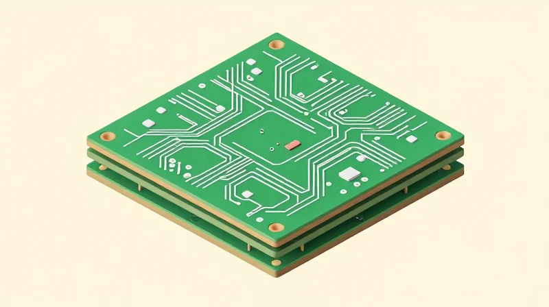
The Architectural Shift to High-Density Interconnect (HDI)
As IIoT sensor nodes evolve to include edge-computing capabilities and sophisticated sensor fusion, traditional through-hole and standard multi-layer PCB designs are becoming obsolete. HDI technology utilizes micro-vias, build-up layers, and finer line/space geometries to achieve a significantly higher interconnect density. This transition allows designers to reduce layer counts and board size, directly addressing the demand for compact, power-efficient industrial edge devices.
Micro-via Advantages in Signal Integrity
The implementation of laser-drilled micro-vias significantly mitigates the parasitic effects associated with traditional through-hole vias. By minimizing via stub length, engineers can drastically reduce signal reflections and electromagnetic interference (EMI) at high frequencies. This is essential for modern sensor architectures that integrate high-speed digital interfaces like MIPI or high-resolution ADC sampling paths.
| Feature | Legacy PCB Process | HDI/Micro-via Technology |
|---|---|---|
| Via Type | Through-hole | Laser-drilled Blind/Buried |
| Component Density | Low/Moderate | Very High |
| Signal Integrity | Limited by Stubs | Excellent for High Speed |
| Layer Count | Higher Requirement | Optimized/Lower |
Frequently Asked Questions on HDI Adoption
- How does HDI improve reliability in harsh environments?
By reducing the total number of layers and minimizing via-related stress points, HDI designs offer superior thermal management and reduced expansion coefficient mismatch during extreme temperature cycling. - Does the transition to micro-vias increase manufacturing costs?
While unit fabrication costs for HDI panels are higher, the overall system cost is often lower due to reduced board footprint, fewer required layers, and higher assembly yields achieved through optimized layout density. - Are there specific design rules for HDI?
Yes, designers must adhere to stricter aspect ratio constraints for laser drilling and account for sequential lamination processes to ensure signal continuity through nested micro-via structures.
Material Science Advancements for Extreme Environments

Beyond FR-4: Material Evolution for Harsh Environments
Legacy FR-4 laminates frequently fail in modern industrial contexts due to limited glass transition temperatures (Tg) and coefficient of thermal expansion (CTE) mismatches. Next-generation sensor architectures are pivoting toward ceramic-filled PTFE, polyimide, and metal-core printed circuit boards (MCPCBs) to provide the structural rigidity and thermal dissipation required for continuous operation in extreme heat and high-vibration environments.
| Feature | Legacy FR-4 | Advanced Substrate (e.g., Ceramic/Metal-Core) |
|---|---|---|
| Thermal Conductivity | Low (0.25 W/mK) | High (2.0 - 5.0+ W/mK) |
| Operating Temperature | Limited (< 130°C) | Extended (> 200°C) |
| Mechanical Stability | Prone to delamination | High resistance to shock/vibration |
| Signal Integrity | Suboptimal at high freq | Excellent (Low loss tangent) |
Thermal Management and Vibration Dampening
Managing heat dissipation at the node level is critical for extending component lifespan. Advanced materials like aluminum nitride and copper-base laminates facilitate heat spreading directly beneath power-hungry components, reducing the reliance on external heat sinking. Furthermore, flexible polyimide substrates offer superior mechanical resilience, allowing sensor nodes to flex under vibration without suffering from trace fracture or solder joint fatigue—a common failure mode in brittle legacy designs.
Frequently Asked Questions
- Why is CTE matching important in extreme environments?
Coefficient of Thermal Expansion matching ensures that the board material and the surface-mounted components expand and contract at the same rate, preventing solder joint cracking during thermal cycling. - Are advanced materials cost-prohibitive for high-volume IIoT?
While unit costs are higher, the reduction in maintenance downtime and the extended operational life of the sensor node result in a lower Total Cost of Ownership (TCO) in harsh industrial settings. - How do these materials impact signal integrity?
Next-gen substrates offer significantly lower dielectric loss and more stable dielectric constants, which are essential for maintaining signal integrity in high-frequency wireless IIoT communication protocols.
The Shift Toward Flexible and Rigid-Flex Architectures
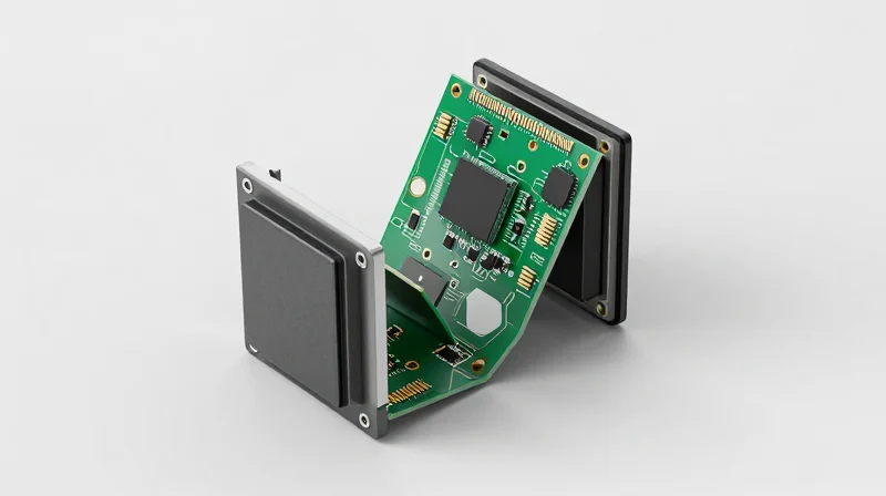
Overcoming Mechanical Constraints with Flexible Circuitry
Traditional rigid FR-4 boards are often the primary bottleneck in IIoT device miniaturization, forcing engineers to sacrifice sensor resolution or power density to fit enclosures. Flexible circuitry fundamentally alters this paradigm by enabling 3D assembly techniques. By utilizing polyimide-based substrates, designers can route circuits around irregular mechanical obstacles, effectively eliminating the need for rigid connectors and bulky wiring harnesses that frequently fail under industrial vibration.
Comparing Rigid, Flex, and Rigid-Flex Architectures
| Feature | Rigid (FR-4) | Flexible | Rigid-Flex |
|---|---|---|---|
| Spatial Efficiency | Low | High | Very High |
| Vibration Resistance | Moderate | Excellent | High |
| Weight | High | Very Low | Low |
| Complexity | Standard | High | Very High |
Strategic Advantages of Rigid-Flex Integration
Rigid-flex circuits provide the structural integrity required for component mounting while offering the flexibility needed for interconnects between disparate segments of a modular sensor node. This hybrid approach significantly reduces the potential points of failure—specifically solder joints and board-to-board connectors—that are notorious for degrading during long-term field deployment in harsh industrial environments.
Frequently Asked Questions
- How does rigid-flex improve reliability over legacy wiring?
Rigid-flex circuits replace unreliable mechanical connectors and discrete wiring harnesses with permanent, chemically-bonded traces, reducing intermittent contact risks caused by thermal cycling and high-frequency vibration. - Are there thermal management tradeoffs with flexible polyimide materials?
While polyimide has lower thermal conductivity than traditional FR-4, modern designs incorporate thermal vias and metal-clad flexible layers to effectively dissipate heat from sensitive processors or power circuitry. - Is the transition to rigid-flex cost-effective for mass production?
While unit costs are higher than standard rigid boards, the total cost of ownership decreases due to reduced assembly labor, fewer interconnect parts, and lower field maintenance costs in IIoT applications.
Design for Manufacturing (DFM) in the Next-Gen Era
Strategic DFM Optimization
As IIoT sensor nodes migrate toward HDI (High-Density Interconnect) and miniaturized form factors, traditional PCB design workflows are no longer sufficient. Designing for modern industrial manufacturing necessitates a deep integration of assembly-level constraints directly into the schematic and layout phases. By prioritizing surface mount technology (SMT) optimization, component standardization, and thermal relief management early, engineers can significantly reduce the 'cost-per-unit' while ensuring high-reliability performance in extreme conditions.
| DFM Focus Area | Legacy Approach | Next-Gen Strategy |
|---|---|---|
| Component Pitch | Large, conservative spacing | Fine-pitch 0.4mm/0.3mm BGA optimization |
| Via Technology | Through-hole drilling | Laser-drilled blind and buried micro-vias |
| Panelization | Manual or basic arraying | Automated Fiducial-driven, panel-optimized designs |
| Assembly | Hand-soldering focus | DFM-verified Pick-and-Place machine compatibility |
Bridging the Gap: FAQ on Modern DFM
- How does HDI design affect manufacturing yield?
While HDI allows for smaller footprints, it requires strict adherence to aspect ratio limits in micro-vias. Properly defined pad geometry and laser-drilling parameters prevent common defects like barrel cracking or incomplete plating, thereby increasing overall yield. - What is the primary constraint when moving to flexible circuitry?
Flexible circuits require specific considerations for bend radii and coverlay stress relief. Designing for flexible materials involves avoiding trace density in bending zones to prevent delamination during vibration-heavy industrial operations. - Why is early SMT collaboration vital for IIoT?
Early collaboration ensures that the component library is optimized for automated assembly processes. This reduces rework, minimizes the need for custom jigs, and ensures the board layout aligns with the manufacturer's specific solder-paste stencil capabilities.
Ultimately, the next-gen industrial sensor node must balance performance with manufacturability. Engineers must treat the manufacturing facility as an extension of their design team, using DFM software checks early in the process to detect potential bottlenecks before the prototype stage. This proactive approach is the only way to scale high-complexity IIoT hardware in a cost-effective, high-volume environment.
Future-Proofing Your Hardware Strategy
Strategic Alignment with Evolving IIoT Standards
Engineers must move beyond component-level selection and adopt a systems-thinking approach that prioritizes longevity and interoperability. Future-proofing is no longer about selecting the most robust capacitor, but about architecting hardware that can accommodate Over-the-Air (OTA) updates, edge-compute scaling, and emerging low-power wide-area network (LPWAN) protocols.
| Strategic Pillar | Legacy Approach | Next-Gen Strategy |
|---|---|---|
| Connectivity | Hardwired/Proprietary | Software-defined/Multimodal |
| Architecture | Monolithic PCB | Modular/Chiplet-based |
| Lifespan | Static Deployment | OTA Firmware-Upgradeability |
| Integration | Vendor Lock-in | Open Standards/API-first |
Key Considerations for Next-Gen Sensor Nodes
- How do we mitigate obsolescence in long-cycle industrial assets?
Implement a modular architecture where the sensor front-end is decoupled from the communication and processing module, allowing for hardware upgrades without replacing the entire installation. - Why is software-defined hardware critical?
As IIoT standards like Matter or OPC UA evolve, hardware must support remote updates to protocol stacks, ensuring that physical sensors do not become obsolete due to shifting communication requirements. - What role does digital twinning play in design?
By maintaining a high-fidelity digital twin during the design cycle, engineers can simulate performance degradation under various industrial stresses, enabling predictive maintenance models that define the node's operational lifespan.
The Path Forward: Modular Lifecycle Management
To achieve long-term viability, design teams must integrate Hardware-in-the-Loop (HIL) testing early in the cycle to validate firmware and hardware interaction under stress. Prioritizing platforms with field-replaceable modules ensures that the physical hardware can evolve alongside the rapidly changing landscape of IIoT connectivity, security, and industrial analytics.
As the IIoT landscape continues to fragment into increasingly complex, high-density applications, the hardware that drives these systems must be robust enough to withstand both environmental stress and rapid technological turnover. By embracing high-reliability, next-gen fabrication strategies, your team can ensure long-term operational success. Ready to transition your sensor nodes to a more reliable, high-density future? Contact our engineering team today for a design audit.
