
The industrial welding sector is undergoing a massive transformation, moving away from bulky, inefficient legacy power systems toward lean, digitized, and highly responsive architectures. As manufacturing demands tighten, the integration of smart power distribution and advanced PCB substrates has become the defining frontier for competitive welding performance.
The Evolution of Welding Hardware: From Legacy to Silicon
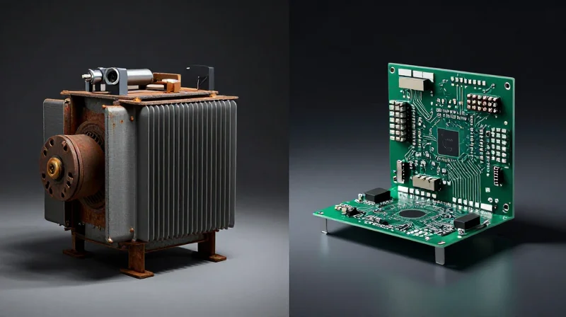
The Era of Heavy Iron: The Limitations of Legacy Systems
For decades, industrial welding relied on massive, copper-wound transformers. These traditional units were built on the principle of raw brute force, converting utility-grade AC power into the high-amperage current necessary to melt metal. While robust and reliable in harsh environments, these systems were inherently inefficient, bulky, and lacked the sophisticated feedback loops required for modern, high-precision manufacturing.
Comparative Overview: Legacy vs. Smart PCB Architecture
| Feature | Legacy Transformer Systems | Smart PCB Power Electronics |
|---|---|---|
| Power Density | Low (Bulky and heavy) | High (Compact and light) |
| Control Speed | Slow (Magnetic saturation limits) | Microsecond (Digital signal processing) |
| Efficiency | Low (High heat loss) | High (Switching mode conversion) |
| Flexibility | Fixed arc characteristics | Programmable wave patterns |
The Silicon Revolution: Smart PCB Integration
The integration of high-power smart Printed Circuit Boards (PCBs) has replaced magnetic regulation with high-frequency electronic switching. By utilizing insulated-gate bipolar transistors (IGBTs) and rapid-response digital microcontrollers, modern welding machines can adjust arc parameters thousands of times per second. This transition enables constant monitoring of the arc environment, resulting in lower spatter, deeper penetration, and the ability to weld exotic materials with consistent metallurgical integrity.
Frequently Asked Questions
- Why is high-frequency switching better?
It reduces the size of the required transformers and inductors while allowing the power source to react instantly to changes in arc voltage, leading to a much more stable weld pool. - Do smart systems require more maintenance?
While traditional units were mechanically simple, smart systems rely on software reliability. Modern industrial PCBs are modular, allowing for faster board-level replacements compared to repairing heavy, burned-out copper coils. - Can smart systems be used in extreme environments?
Yes, provided the electronics are properly potted or conformal-coated to resist dust, humidity, and conductive particles that typically affect PCB longevity.
Anatomy of Modern High-Power PCBs
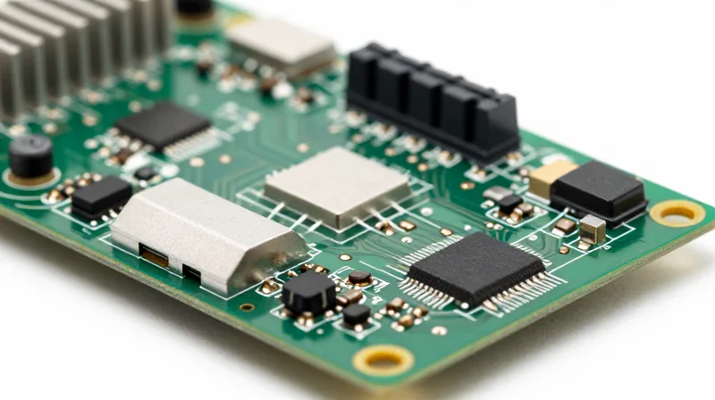
The transition from bulky, transformer-based power delivery to sophisticated, high-power printed circuit boards (PCBs) is defined by a radical shift in electrical architecture. Modern industrial welding boards are engineered to act as the central nervous system of the welder, facilitating rapid switching, real-time feedback, and massive current throughput while minimizing heat-induced degradation.
Critical Structural Components
- Heavy-Copper Internal Layers
Modern boards utilize 3oz to 6oz copper weights, significantly thicker than standard electronics, to manage high-amperage flow without excessive resistive heating. - Ceramic-Filled Laminates
These specialized substrates provide superior thermal conductivity compared to standard FR-4, effectively drawing heat away from power-dense silicon components. - Integrated Thermal Vias
High-density arrays of plated through-holes act as vertical heat pipes, conducting thermal energy from high-heat components to secondary heat sinks or baseplates.
Comparative Thermal Management: Traditional vs. Modern
| Feature | Traditional Design | High-Power Smart PCB |
|---|---|---|
| Switching Speed | Low (Line Frequency) | High (kHz range) |
| Thermal Path | Air-cooled heavy copper busbars | Integrated ceramic substrate conduction |
| Heat Dissipation | Passive/Convection | Active thermal via management |
| Integration | Modular discrete components | System-on-chip with embedded sensors |
Intelligent Monitoring Architecture
Beyond physical construction, the modern PCB serves as a sensor fusion platform. By integrating hall-effect current sensors and localized thermistors directly onto the board substrate, the system can adjust switching cycles in microseconds. This prevents current spikes before they can cause localized delamination or solder joint fracture, a common failure point in legacy hardware.
Technical Specifications Overview
PCB_Parameters = {
  'Cu_Weight': '4oz_min',
  'Substrate': 'Metal_Core_PCB',
  'Thermal_Vias': 'High_Density_Array',
  'Sensor_Sampling_Rate': '100kHz'
}
The Role of Advanced Substrate Materials
Beyond FR-4: The Thermal Bottleneck
Standard FR-4 fiberglass substrates, while cost-effective for consumer electronics, possess poor thermal conductivity, which leads to localized heat entrapment during high-current welding cycles. In industrial environments where power densities exceed 50A per trace, traditional boards face catastrophic delamination and dielectric breakdown. Transitioning to Metal Core Printed Circuit Boards (MCPCBs) or specialized ceramic substrates provides the necessary heat dissipation paths to maintain device longevity under extreme duty cycles.
Comparative Analysis: Substrate Material Performance
| Material Type | Thermal Conductivity (W/mK) | Industrial Suitability | Durability |
|---|---|---|---|
| Standard FR-4 | 0.25 - 0.3 | Low (Control Logic Only) | Low |
| Aluminum Core (MCPCB) | 1.0 - 3.0 | Moderate (Welding Power Stages) | High |
| Ceramic (Alumina/AlN) | 20.0 - 200+ | Extreme (High-Frequency Inverters) | Very High |
Key Advantages of Advanced Substrates
- Thermal Expansion Matching
Ceramic substrates offer coefficient of thermal expansion (CTE) values closer to silicon power chips, significantly reducing mechanical stress and solder joint fatigue during rapid heating and cooling. - Voltage Isolation
These substrates provide superior dielectric strength, allowing for tighter component spacing without the risk of arcing in high-voltage industrial welding environments. - Size Reduction
Improved thermal dissipation allows for higher power density in a smaller footprint, enabling the development of portable, high-capacity welding units that outperform legacy transformer-based designs.
Integration Challenges and Future Outlook
While ceramic and metal-core substrates represent the future of industrial welding, their integration requires advanced manufacturing processes including specialized thermal interface materials (TIM) and precision laser-cutting. As the demand for more intelligent, responsive welding systems increases, the industry is shifting toward these high-performance substrates as the standard for ensuring reliability in the harshest factory conditions.
Precision Power Distribution and Machine Responsiveness

Precision Power Distribution and Machine Responsiveness
The transition from mechanical reactors to intelligent PCB-driven power distribution has fundamentally redefined machine responsiveness. By employing high-frequency switching technology, modern welding systems can modulate power delivery in the micro-second range, allowing the machine to react to changes in the arc environment before the human eye or standard sensors can even register a shift.
Micro-second Modulation vs. Legacy Systems
Traditional transformer systems rely on high-inductance iron cores that inherently resist rapid changes in current. In contrast, modern high-power PCBs utilize MOSFET or IGBT arrays that switch at frequencies exceeding 100 kHz. This capability enables precise control over the droplet transfer process, significantly reducing spatter and increasing penetration depth consistency.
| Feature | Legacy Transformer | Smart PCB System |
|---|---|---|
| Response Time | 10 - 50 Milliseconds | 1 - 10 Microseconds |
| Current Control | Passive/Mechanical | Active/Software-defined |
| Arc Stability | Variable based on line load | Consistent via active feedback |
Common Questions on PCB-Driven Responsiveness
- How does high-frequency switching improve weld quality?
By switching at high frequencies, the system can perform real-time adjustments to the voltage wave shape, which optimizes the burn-off rate of the electrode and ensures a smoother, more uniform weld bead. - Can smart PCBs compensate for fluctuating input power?
Yes, intelligent circuitry detects input voltage drops instantaneously and modulates the gate drive signals to maintain a constant output current at the arc, ensuring stability even in weak power grids.
Energy Efficiency and Sustainability Metrics
Quantifying Energy Efficiency in Smart Welding Systems
Traditional welding machines, reliant on bulky copper-wound transformers and magnetic ballast systems, suffer from high idle power consumption and substantial heat dissipation losses. In contrast, modern high-power smart PCB architectures utilize high-frequency switching technology and Insulated Gate Bipolar Transistors (IGBTs) to modulate power precisely at the micro-second level. This transition from 'brute force' power management to 'intelligent' regulation minimizes electrical resistance, reduces thermal waste, and significantly lowers the overall duty-cycle energy demand.
| Metric | Traditional Transformer Units | Smart PCB-Based Units |
|---|---|---|
| Energy Conversion Efficiency | 70-80% | 90-95% |
| Idle Power Consumption | High (Continuous Excitation) | Negligible (Sleep/Standby Modes) |
| Carbon Footprint (Lifecycle) | High (Heavy Metal Usage) | Low (Modular Design/Component Efficiency) |
| Heat Waste Generation | Excessive | Minimal (Advanced Cooling Management) |
Sustainability and Industrial Longevity
The environmental impact of welding equipment extends beyond electricity consumption. Traditional units are heavy, resource-intensive to manufacture, and often require complete replacement due to internal transformer degradation. Smart PCB systems offer modularity; individual power modules can be upgraded or replaced, extending the machine's operational lifespan. Furthermore, the integration of real-time monitoring software allows facility managers to optimize arc behavior, which reduces material wastage from defective welds, thereby contributing to broader ESG (Environmental, Social, and Governance) targets.
FAQ: Energy and Sustainability
- How does PCB technology reduce carbon emissions?
By increasing conversion efficiency, smart PCBs require less electricity from the grid for the same welding output, directly correlating to lower Scope 2 carbon emissions. - Can software updates improve power efficiency?
Yes. Smart systems allow for firmware optimization of switching frequencies, allowing machines to adapt their power profile to match specific materials, preventing unnecessary energy draw. - Is the production of high-power PCBs more harmful to the environment?
While PCB fabrication involves chemical processes, the reduced lifecycle consumption of energy and lower material weight for equivalent output typically offsets the production footprint within the first year of operation.
Reliability and Thermal Management in High-Load Environments
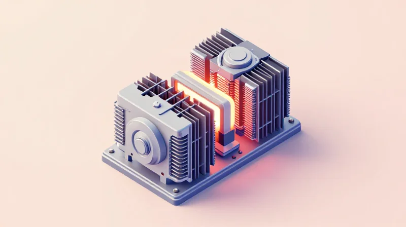
Mitigating Thermal Stress and Component Fatigue
Reliability in high-load industrial welding is primarily dictated by the system's ability to manage heat dissipation during extended duty cycles. Traditional welding designs often rely on bulky, analog cooling systems and large passive components that are highly susceptible to thermal fatigue. Conversely, modern high-power smart PCB architectures utilize integrated thermal sensors and advanced heat sinking strategies to maintain optimal operating temperatures, significantly reducing the mechanical strain on sensitive power electronics.
| Feature | Traditional Design | Smart PCB Technology |
|---|---|---|
| Thermal Regulation | Passive / Mechanical | Active / Predictive |
| Failure Mode | Component Thermal Fatigue | Software-controlled Derating |
| System Maintenance | Frequent / Reactive | Predictive / Low-Interval |
Long-Term Operational Economics
Beyond immediate performance gains, the transition to smart PCB technology yields substantial cost benefits over the lifecycle of the welding equipment. By preventing localized overheating and dampening power surges that lead to premature component failure, manufacturers can significantly reduce downtime costs and repair frequency.
- How does smart PCB design specifically extend component life?
By utilizing precision power modulation and real-time thermal monitoring, the system keeps components operating within their ideal temperature window, preventing the micro-cracking and solder fatigue common in legacy systems. - Does the increased complexity of smart PCBs introduce new points of failure?
While modern designs are more complex, the high level of integration and use of solid-state components typically result in lower failure rates compared to legacy analog components that are prone to mechanical degradation. - What is the primary driver of cost savings in high-load environments?
The primary drivers are the reduced need for unscheduled maintenance, fewer replacement parts, and improved energy efficiency that compounds over thousands of hours of high-amperage welding.
Integrating Industry 4.0: Data-Driven Welding
The Shift to Data-Driven Welding
Integrating Industry 4.0 principles via high-power smart PCBs shifts the role of the welding machine from a simple power source to an intelligent node within a manufacturing ecosystem. By embedding high-speed microprocessors directly into the power electronics, manufacturers can capture granular data at the arc level, providing transparency that traditional systems simply cannot offer.
Predictive Maintenance and Real-Time Feedback
Smart PCBs facilitate continuous monitoring of electrical signatures and thermal profiles, allowing systems to detect early signs of component drift. This predictive capability identifies potential failures before they result in equipment downtime, ensuring that maintenance is performed based on machine health rather than arbitrary schedules.
| Feature | Traditional Welding | Smart PCB Welding |
|---|---|---|
| Data Visibility | None (Analog gauges only) | Real-time digital logging |
| Maintenance Approach | Reactive/Scheduled | Predictive/Condition-based |
| Error Detection | Manual Inspection | Automated ARC monitoring |
| Connectivity | Isolated | IIoT/Cloud integrated |
Frequently Asked Questions
- How do smart PCBs improve welding quality control?
They track parameters like voltage, current, and wire feed speed in real-time, matching them against established golden-weld profiles to identify defects instantly. - Does real-time data collection require high-end IT infrastructure?
Modern smart welding units are designed with standard communication protocols, allowing for seamless integration into existing industrial Ethernet and IIoT gateways. - Can smart PCBs retroactively upgrade legacy machines?
While often built into new hardware, some modular smart PCB interfaces can be adapted to enhance performance monitoring for older equipment, though full integration is most effective in new-generation units.
The Future Outlook for Welding Infrastructure
The Trajectory of PCB Miniaturization in Industrial Settings
Future industrial welding infrastructure will be defined by the radical reduction of internal component footprints. As high-power smart PCBs achieve higher power densities, we anticipate a transition from bulky, centralized power sources to modular, distributed welding cells. These compact units can be integrated directly onto robotic arms or gantry systems, minimizing cable losses and enabling ultra-low-latency response times for high-speed automated processes.
Infrastructure Evolution: Traditional vs. Smart Architecture
| Feature | Traditional Infrastructure | Smart PCB Architecture |
|---|---|---|
| Component Scale | Large, centralized power banks | Miniaturized, edge-compute modules |
| System Feedback | Analog/Manual adjustment | AI-driven predictive loop |
| Integration | Isolated stand-alone stations | Hyper-connected IoT ecosystem |
| Maintenance | Reactive hardware replacement | Proactive, software-defined patches |
AI-Driven Control and Autonomous Calibration
The next generation of infrastructure will not merely execute welds but interpret them. Smart PCBs will incorporate local AI accelerators to perform real-time thermal analysis, adjusting voltage and wire feed speeds at sub-millisecond intervals. This capability removes the dependency on human intervention for minor process drift, effectively turning each welding station into an autonomous agent within the factory floor.
Frequently Asked Questions on Future Infrastructure
- How will smart PCBs impact long-term facility costs?
While initial investment in smart PCB infrastructure is higher, total cost of ownership (TCO) is reduced through energy efficiency, drastically lower downtime via predictive maintenance, and increased weld throughput. - Can current legacy welding setups be retrofitted with smart technology?
Partial retrofitting is possible through secondary sensing units, but full benefits are only realized by migrating to native smart-PCB power sources designed for direct AI communication. - What is the role of 5G and edge computing in this transition?
High-speed networking allows for the synchronization of entire welding cells, enabling factory-wide optimization where hundreds of smart units coordinate to balance power loads and production schedules.
By embracing high-power smart PCB technology, manufacturers can significantly reduce energy waste, boost weld quality, and extend the lifespan of their equipment. As industry standards rise, upgrading your infrastructure is not just an improvement; it is a competitive necessity. Contact our engineering team today to learn how our custom PCB solutions can modernize your production line.
