
As the demand for hyper-compact, high-performance electronics reaches an all-time high, the architecture of our Printed Circuit Boards must evolve. Traditional through-hole designs, while reliable, are hitting a ceiling in the face of modern signal integrity requirements and shrinking form factors. This guide explores the critical transition to High-Density Interconnect (HDI) structures and explains why blind and buried vias are the essential building blocks for tomorrow’s hardware.
Understanding the Traditional Through-Hole Limitation
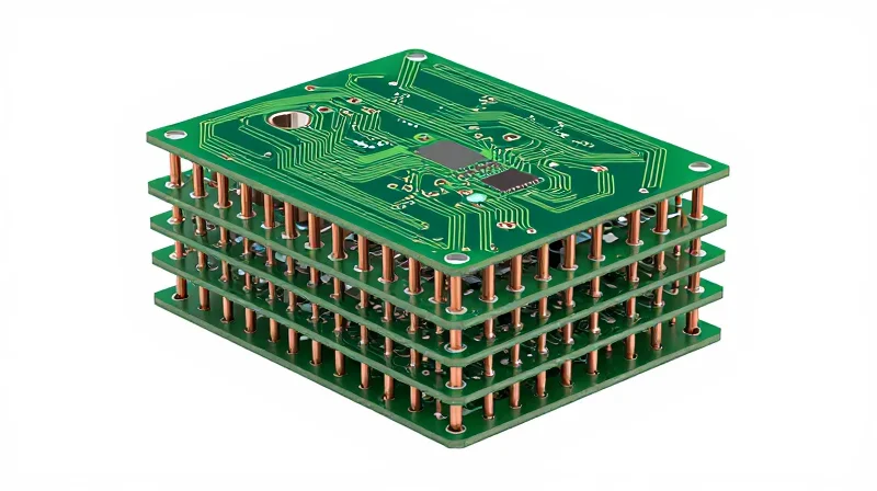
The Geometric Constraints of Through-Hole Vias
Traditional through-hole technology relies on drilling a path through every layer of a printed circuit board to create an electrical connection. While this method remains a standard for simplicity and cost, it introduces a significant structural footprint that limits design density. Because a single through-hole via occupies space on every layer, it creates 'keep-out' zones that prevent the routing of traces, effectively reducing the available real estate for high-speed signal paths.
Impact on Signal Integrity and Routing
Beyond the consumption of surface area, through-hole vias create electrical discontinuities known as stubs. A stub is the unused portion of the via barrel that extends beyond the required signal path. At high frequencies, these stubs act as capacitive antennas, reflecting signals and introducing parasitic inductance, which significantly degrades signal integrity.
| Limitation Category | Through-Hole Impact | Design Consequence |
|---|---|---|
| Spatial Efficiency | Layer-to-layer penetration | Increased keep-out areas and trace congestion |
| Electrical Performance | Stray stub capacitance | Signal reflection and EMI issues |
| Routing Complexity | Vertical path requirements | Longer trace paths and increased impedance mismatch |
- Why do through-hole vias limit high-speed design?
The excess length (stubs) in a through-hole via creates parasitic capacitance that acts as a low-pass filter, limiting the maximum achievable data rate of the interconnect. - How does through-hole technology affect routing density?
Each via traverses every layer, creating a circular keep-out zone on every signal plane. This forces designers to use longer, more convoluted traces to route around these physical barriers.
The Rise of High-Density Interconnect (HDI) Architecture

The Paradigm Shift to HDI Architecture
As the demand for complex, compact electronic devices accelerates, traditional through-hole PCB designs have become a bottleneck. HDI architecture provides the solution by utilizing micro-vias, build-up laminates, and finer trace pitches to drastically increase routing density, allowing for smaller, lighter, and more performance-driven circuit boards.
Why HDI is Essential for Modern Electronics
Modern high-speed data transmission requires signal paths that are as short as possible to minimize parasitic effects like capacitance and inductance. HDI supports this by enabling point-to-point connections within internal layers, effectively reducing signal reflection and crosstalk compared to conventional through-hole designs that utilize long, inefficient stubs.
| Feature | Through-Hole PCB | HDI PCB |
|---|---|---|
| Via Technology | Plated Through-Hole (PTH) | Micro-via (Blind/Buried) |
| Layer Count | Generally Lower | Higher Density |
| Space Efficiency | Low (large footprint) | High (compact footprint) |
| Signal Integrity | Prone to signal stubs | Excellent for high speed |
Frequently Asked Questions
- How does HDI improve signal integrity?
By using blind and buried micro-vias instead of through-hole vias, HDI eliminates the long, unused barrel portions of a via known as stubs. These stubs typically cause signal reflections at high frequencies, which are effectively negated in HDI designs. - Is HDI only used for small mobile devices?
While popular in mobile devices for miniaturization, HDI is increasingly used in high-performance computing, medical equipment, and automotive electronics to manage high-density BGA components and high-speed data signal paths. - Does the transition to HDI increase manufacturing costs?
HDI manufacturing generally involves higher initial costs due to the need for advanced equipment (such as laser drilling) and stricter alignment tolerances. However, the total cost of ownership is often lower due to reduced PCB size and improved system functionality.
Anatomy of Blind and Buried Vias
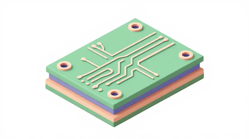
Anatomy of Blind and Buried Vias
Blind and buried vias represent a fundamental departure from through-hole technology by allowing connections between specific board layers without penetrating the entire stack-up. A blind via connects an outer layer to an internal layer but does not reach the opposite side, while a buried via is entirely contained within the internal layers, connecting two or more inner layers without reaching the board surface. By isolating electrical paths, these interconnects reduce parasitic inductance and free up significant real estate on outer layers for component placement.
Fabrication Distinctions
The fabrication of these vias requires sophisticated sequential lamination processes. Unlike through-hole vias, which are drilled after the entire stack is laminated, blind and buried vias are drilled and plated in stages. This increases manufacturing complexity and cost but is essential for supporting the high pin densities required by modern BGA (Ball Grid Array) components.
| Feature | Through-Hole | Blind Via | Buried Via |
|---|---|---|---|
| Layer Access | Entire Stack | Outer to Inner | Internal Layers |
| Drilling Process | Single Pass | Sequential | Sequential |
| Surface Area | High Consumption | Minimal | Zero |
| Inductance | Higher | Lower | Lowest |
Technical FAQs
- How do blind and buried vias improve signal integrity?
By eliminating unused barrel length (stubs) inherent in through-hole designs, these vias reduce capacitive and inductive reflections, which is critical for high-speed signal transmission. - Why is the cost higher for these interconnects?
The requirement for sequential lamination, individual drilling cycles, and additional inspection steps significantly increases the time and complexity of the PCB manufacturing process. - Are there specific design rules for these structures?
Designers must strictly adhere to aspect ratio limitations defined by the fabricator, as laser-drilling deep or narrow vias involves specific geometry constraints to ensure reliable copper plating.
Performance Benefits: Signal Integrity and EMI Control
Mitigating Signal Distortion Through Stub Removal
In traditional through-hole technology, a signal traversing between internal layers leaves behind a residual via stub—the unused portion of the barrel extending from the signal layer to the board surface. At high gigabit frequencies, these stubs act as open-circuited transmission line resonators. This phenomenon creates severe signal degradation characterized by sharp notches in the frequency response, leading to jitter and bit error rate (BER) increases. Blind and buried vias eliminate these stubs entirely, ensuring the signal path is optimized for high-speed propagation without resonant interference.
Comparative Impact on Parasitics and EMI
| Parameter | Through-Hole Vias | Blind/Buried Vias |
|---|---|---|
| Parasitic Capacitance | High (due to via length) | Low (minimized geometry) |
| Inductive Stub Effect | Significant (Resonant notches) | Negligible (Stub-free paths) |
| EMI Radiation Potential | High (Acts as an antenna) | Low (Controlled internal routing) |
| Propagation Delay | Higher (Due to excess length) | Lowest (Direct signal path) |
EMI Control and Electromagnetic Compatibility
Beyond pure signal integrity, EMI management is critical for high-density architectures. Long through-hole barrels act as unintentional antennas, radiating electromagnetic energy that can couple into adjacent traces or create system-level compliance issues. Blind and buried vias allow designers to keep signal transitions contained within the internal board layers. By reducing the physical size of the current return loop and avoiding surface-reaching via barrels, engineers can significantly reduce common-mode noise and improve overall system-level EMI shielding.
Frequently Asked Questions
- How does via stub length affect data rates?
As data rates increase, even small stubs reach their resonant frequency, causing signal attenuation. Removing these stubs via blind/buried interconnects is essential for frequencies above 5-10 GHz. - Do buried vias help with layer-to-layer crosstalk?
Yes, buried vias allow for more controlled vertical routing between internal layers, providing better proximity to ground planes and reducing the footprint of high-speed signals on outer layers. - Is the transition to HDI worth the fabrication cost?
While fabrication is more expensive, the performance reliability and ability to meet high-speed signal integrity standards make blind/buried vias the only viable choice for modern high-performance electronics.
Space Efficiency and Component Density
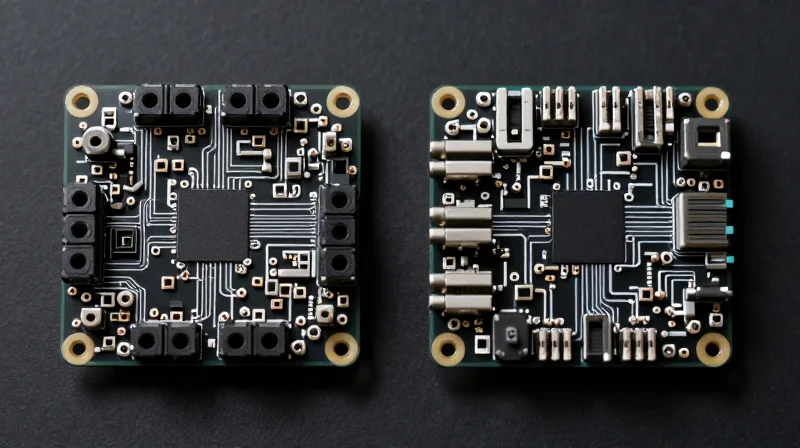
Maximizing Real Estate Through Vertical Integration
The primary limitation of traditional Through-Hole (PTH) technology is the 'via footprint'—the physical exclusion zone required around every hole to ensure structural integrity and pad clearance. Because PTH vias traverse every layer of the PCB, they consume routing channels on layers where they serve no electrical function. By contrast, blind and buried vias are confined to specific sub-layers, effectively decoupling the routing requirements of different signal groups. This vertical partitioning allows designers to stack components more tightly and utilize internal board area that would otherwise be rendered unusable by through-hole barrels.
Comparative Efficiency of Via Architectures
| Feature | Through-Hole (PTH) | Blind/Buried Vias |
|---|---|---|
| Routing Blockage | High (Affects all layers) | Low (Localized to specific layers) |
| Component Density | Low/Moderate | High/Ultra-High |
| PCB Surface Area Usage | High (Large landing pads) | Optimized (Via-in-Pad capability) |
| Complexity/Cost | Low | High |
The Role of Via-in-Pad Technology
Advanced density is further achieved through Via-in-Pad (VIP) structures. By plating the via hole and filling it with conductive or non-conductive epoxy, designers can place the via directly beneath BGA (Ball Grid Array) pads. This eliminates the need for 'dog-bone' fanout patterns, which typically consume significant surface area. Integrating these vias allows for a tighter pitch on fine-grid components, directly reducing the required footprint for high-pin-count processors and memory modules.
Design Efficiency FAQ
- How do buried vias specifically aid density?
Buried vias connect only internal layers, allowing for 'hidden' routing paths that do not disrupt the signal integrity of the top or bottom layers, thus doubling the available routing space on inner planes. - Can blind/buried vias replace all through-hole connections?
While they maximize density, they do not always replace through-holes; instead, they work in conjunction with PTH for power and ground planes where large currents require robust, through-the-board thermal and electrical paths. - Does higher component density create thermal challenges?
Yes, increased density creates localized heat pockets. Designers must utilize thermal vias or metal-filled blind vias to effectively conduct heat to ground planes or external heatsinks.
Thermal Management and Reliability Considerations
Thermal Dissipation Challenges in High-Density Designs
While blind and buried vias facilitate superior routing density, their compact geometry limits natural heat conduction paths compared to traditional through-hole vias. In standard designs, through-hole barrels act as thermal conduits, channeling heat from surface components to internal planes. In high-density interconnects (HDI), the absence of a continuous copper path through the entire board thickness forces engineers to rethink thermal dissipation strategies, often requiring integrated micro-vias or dedicated thermal pads.
| Metric | Through-Hole Via | Blind/Buried Via |
|---|---|---|
| Thermal Conductivity | High (Continuous Path) | Low (Localized/Discontinuous) |
| Mechanical Stress | Lower (Uniform Distribution) | Higher (CTE Mismatch Risk) |
| Routing Flexibility | Limited | Excellent |
Reliability and Mechanical Integrity
Mechanical reliability in multilayer boards is governed by the coefficient of thermal expansion (CTE) mismatch between the copper vias and the dielectric substrate. Blind and buried vias, due to their smaller aspect ratios and the sequential nature of their fabrication, are subject to significant vertical shear stresses during thermal cycling. Proper stack-up design and the selection of materials with matched CTEs are essential to preventing barrel cracking or pad delamination in high-density builds.
Common Reliability Questions
- How do we compensate for the thermal limitations of buried vias?
Engineers often employ thermal micro-via arrays under high-power components and utilize high-conductivity thermally conductive prepregs to bridge gaps. - Do blind vias face higher failure rates under vibration?
Smaller, non-penetrating structures are actually more robust against board flexing, provided the plating thickness within the via is strictly controlled and free of voids. - Is via-filling necessary for reliability?
Yes, copper-filled or conductive epoxy-filled vias are recommended to reduce entrapped air and improve mechanical support, which directly enhances long-term reliability under thermal stress.
Cost-Benefit Analysis for Modern Hardware Projects
The transition from traditional Through-Hole Technology (THT) to advanced interconnect structures involving blind and buried vias represents a paradigm shift in PCB economics. While THT offers the lowest fabrication cost per unit, high-performance applications often demand the signal integrity and routing density provided by HDI (High-Density Interconnect) techniques. Choosing between these technologies requires a rigorous analysis of total cost of ownership, including prototyping speed, assembly yield, and long-term product reliability.
Cost Drivers in PCB Interconnect Architecture
| Metric | Traditional Through-Hole | Blind/Buried Via HDI |
|---|---|---|
| Fab Complexity | Low | High |
| Cost per Layer | Baseline | 30% - 60% Premium |
| Board Size | Larger footprint | Compact/High density |
| Assembly Yield | High | Requires tighter tolerances |
Strategic Justification for Advanced Vias
The premium associated with blind and buried vias is rarely just an expense; it is a strategic investment in miniaturization. By enabling via-in-pad designs and reducing layer count requirements through improved trace density, engineers can often downsize the physical dimensions of the PCB. This reduction in raw material consumption—specifically substrate and copper laminate—can partially offset the higher fabrication costs of laser-drilled interconnects.
- When is the cost premium justified?
When signal integrity requirements for high-speed data transmission outweigh standard routing capabilities, or when the final product size constraints dictate an unavoidable increase in component density. - Does HDI increase assembly costs?
Yes, high-density designs often necessitate tighter alignment tolerances and sophisticated inspection processes, which can increase the overhead costs for Surface Mount Technology (SMT) assembly lines. - How does volume influence the decision?
In low-volume prototypes, the design flexibility of HDI can save time and iterations. In mass production, the high recurring cost of advanced drilling must be weighed against the potential savings from reduced board surface area.
Ultimately, the decision matrix hinges on the performance ceiling of the design. If a through-hole design forces a board size increase that drives up enclosure costs or compromises signal bandwidth, the cost-benefit analysis will heavily favor the adoption of blind and buried vias despite their increased manufacturing complexity.
Future-Proofing Your Design Roadmap

Building a Resilient Design Roadmap
To remain competitive in the rapidly evolving hardware landscape, engineers must shift from monolithic through-hole designs toward modular, HDI-centric frameworks. Future-proofing necessitates the early adoption of blind and buried via technologies, which allow for greater signal integrity and space optimization. By designing for scalability today, firms avoid the prohibitive costs of redesigning legacy PCBs when components inevitably transition to finer-pitch packages.
Strategic Technology Adoption Metrics
| Strategic Consideration | Through-Hole Focus | HDI/Advanced Via Focus |
|---|---|---|
| Signal Integrity | High parasitic reactance | Optimized impedance control |
| Board Real Estate | Limited density | Maximum component throughput |
| Future Compatibility | Legacy/Low-speed | Next-gen high-speed/RF |
| Manufacturing Cost | Low entry barrier | High efficiency at scale |
Common Strategic Inquiries
- How do I mitigate the risk of switching to advanced vias?
Early engagement with your fabrication partner is critical; conduct Design for Manufacturing (DFM) reviews to ensure the selected via aspect ratios are within current process capabilities. - Is it worth upgrading every project?
No; prioritize HDI for projects with space constraints or high-speed requirements, while reserving traditional methods for simple, low-cost utility boards. - How does via technology affect long-term maintenance?
Advanced via structures improve reliability by reducing thermal fatigue and mechanical stress compared to high-aspect-ratio through-hole barrels.
The transition to advanced interconnect technology is no longer a luxury but a necessity for competitive edge in the consumer electronics landscape. By embracing blind and buried vias, engineers can break free from the constraints of legacy designs. Contact our engineering team today to optimize your next PCB project for performance and scalability.
