
As modern industrial electronics shrink in size and grow in complexity, the old methods of shielding sensitive components are being pushed to their absolute limits. Engineers are now forced to choose between the bulk of traditional potting and the precision of next-generation protective barriers. This article cuts through the noise to help you select the right strategy for your next mission-critical hardware design.
The Evolution of PCB Protection Requirements
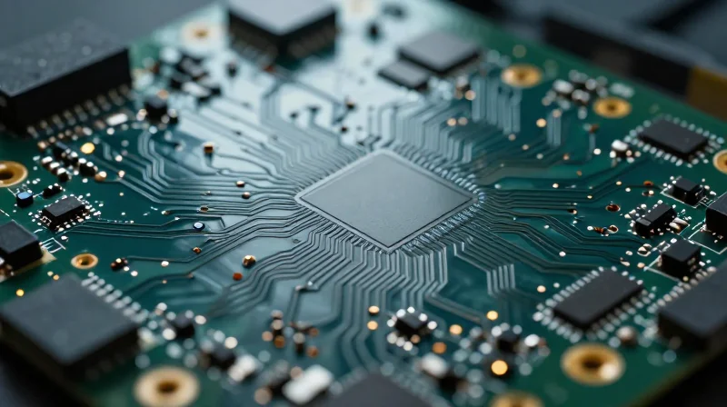
From Bulk Protection to Precision Engineering
Historically, PCB protection relied on heavy, monolithic approaches like full encapsulation potting. While effective at providing a brute-force shield against environmental hazards, the transition toward high-density interconnects (HDI) and the widespread adoption of miniaturized surface-mount devices (SMDs) have rendered traditional heavy potting increasingly untenable. Modern electronic designs demand protection that does not compromise signal integrity, thermal dissipation, or the weight requirements of modern portable and aerospace devices.
The Impact of Miniaturization on Protection Standards
The push toward finer pitch components and multi-layer boards has created two distinct challenges for protection materials. First, the reduction in component spacing makes mass-application potting difficult to control, risking the formation of voids that trap heat or contaminants. Second, the higher power densities associated with HDI designs require thermal management paths that thick, insulating potting compounds often obstruct. Consequently, the industry is trending toward thinner, precision-applied conformal coatings that provide targeted protection without the thermal penalty of traditional mass-casting methods.
| Parameter | Traditional Potting | Modern Conformal Coatings |
|---|---|---|
| Thickness | High (Millimeters) | Low (Microns) |
| Thermal Impedance | High | Low |
| Weight Impact | Significant | Negligible |
| Reworkability | Difficult to Impossible | Generally Possible |
- Why is mass potting falling out of favor in HDI designs?
The high coefficient of thermal expansion (CTE) mismatch between dense potting compounds and fragile miniaturized components often leads to solder joint fatigue during thermal cycling. - How do advanced coatings manage the heat of modern processors?
Unlike bulk potting, which traps heat across the entire assembly, thin-film conformal coatings allow for direct airflow or secondary heatsink contact, significantly improving thermal performance.
Understanding Traditional Potting Compounds
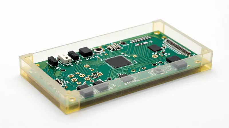
The Mechanics of Traditional Potting
Traditional potting involves encapsulating a PCB within a solid or gel-like resin, such as epoxy or silicone, to create a robust barrier against moisture, vibration, and chemical ingress. While these compounds provide unparalleled structural rigidity and environmental sealing, they fundamentally alter the physical profile of the electronics assembly, presenting significant challenges for contemporary, high-density applications.
Key Material Limitations
The primary drawback of traditional potting stems from the material mass and thermal behavior. Because potting fills the entire housing volume, it introduces significant weight—a critical disadvantage in aerospace and portable device sectors. Furthermore, the difference in the Coefficient of Thermal Expansion (CTE) between the resin and the PCB components often induces mechanical stress during temperature cycling, leading to potential solder joint fatigue.
| Attribute | Epoxy Potting | Silicone Potting |
|---|---|---|
| Hardness | Very High (Rigid) | Low to Medium (Flexible) |
| Repairability | Near Impossible | Difficult (Mechanical removal) |
| Thermal Expansion | Low/Moderate | High |
| Weight Impact | Significant | Significant |
Common Questions Regarding Potting
- Can potted PCBs be repaired?
In almost all cases, no. The encapsulation process is intended to be permanent. Attempting to remove rigid epoxy often destroys the delicate components and traces underneath. - How does potting affect thermal management?
While some potting compounds are thermally conductive, they generally trap heat compared to convection-cooled systems. The bulk mass acts as a thermal buffer, which can be beneficial or detrimental depending on the heat dissipation path of the specific design. - Why is CTE mismatch a risk?
As temperatures fluctuate, the potting compound and the PCB materials expand and contract at different rates, placing mechanical tension on leads and solder joints, eventually leading to cracks.
The Rise of Vapor Deposition
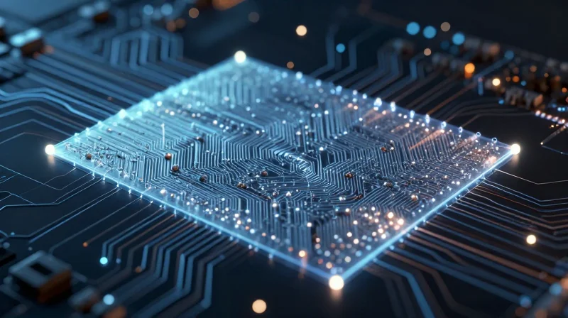
The Rise of Vapor Deposition
As electronic assemblies evolve toward higher component density and more complex, low-profile architectures, traditional liquid-applied coatings often fail to provide consistent protection. Vapor deposition, specifically Chemical Vapor Deposition (CVD) used for polymers like Parylene, addresses these challenges by transforming a solid dimer into a gaseous monomer that polymerizes on the substrate. This process ensures that the protective barrier penetrates underneath SMT components, fills narrow gaps, and wraps around sharp edges with uniform thickness, creating a true pinhole-free encapsulation.
Vapor Deposition vs. Traditional Methods
| Feature | Vapor Deposition (Parylene) | Traditional Potting |
|---|---|---|
| Application Method | Vacuum Chamber (Gas) | Dispensing/Pouring (Liquid) |
| Layer Thickness | Micron-level (Uniform) | Millimeter-level (Bulk) |
| Weight Impact | Negligible | Significant |
| Coverage | Conformal/Pinhole-free | En Masse/High Stress |
Key Advantages for Modern Electronics
- How does vapor deposition achieve superior coverage?
Because the material is in a gaseous state during application, it achieves molecular-level penetration, allowing it to coat the underside of components and complex geometries that liquid coatings cannot reach due to surface tension. - Does this process impact thermal management?
No. The ultra-thin nature of vapor-deposited layers minimizes thermal resistance, allowing for better heat dissipation compared to the thick, insulating bulk of traditional potting compounds. - Is vapor deposition suitable for miniaturized components?
It is the ideal solution. It provides robust environmental protection for MEMS, sensors, and HDI boards without adding the significant mass or mechanical stress associated with traditional potting.
Harnessing UV-Curable Conformal Coatings
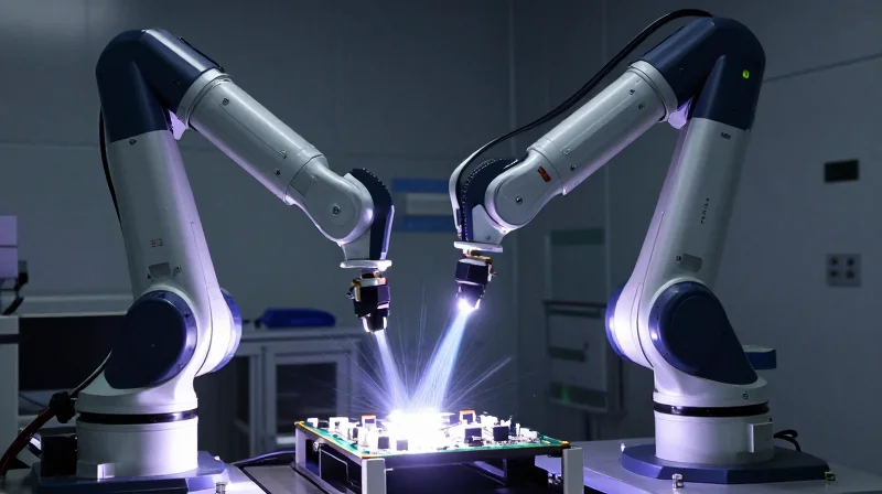
The Advantages of Rapid-Cure UV Technology
UV-curable conformal coatings have emerged as a dominant force in high-volume electronics manufacturing, primarily due to their ability to undergo polymerization in seconds upon exposure to specific ultraviolet wavelengths. Unlike traditional moisture-cure or solvent-based systems that require lengthy air-drying or thermal oven cycles, UV-curable chemistries offer an instantaneous transition from liquid to solid, drastically reducing work-in-progress inventory and footprint requirements.
Performance Comparison: UV Coatings vs. Traditional Potting
| Feature | UV-Curable Coating | Traditional Potting |
|---|---|---|
| Cure Speed | Seconds | Hours to Days |
| Weight/Mass | Negligible | High |
| Process Footprint | Small (Conveyor) | Large (Batch Oven) |
| Reworkability | High | Low/Impossible |
| Cost-Efficiency | High Volume Ideal | Low Volume Ideal |
Critical Implementation Considerations
While UV-curable materials provide significant throughput gains, they require precise application control to ensure complete coverage on boards with high-density components. Shadowing—where the component geometry prevents UV light from reaching the coating—remains a technical challenge. Leading manufacturers solve this by utilizing dual-cure systems, which combine an initial UV-snap cure with a secondary moisture or heat-cured mechanism to reach underneath component leads and shadowed regions.
- How do UV coatings handle component shadowing?
Engineers often specify dual-cure materials. The UV stage locks the position of the coating, while the secondary curing stage ensures complete polymerization in areas hidden from direct light. - Are UV coatings effective against extreme moisture?
Yes, modern UV-cured formulations provide excellent dielectric properties and moisture resistance, often matching or exceeding standard acrylic or polyurethane alternatives while maintaining a much lower profile. - What is the biggest operational benefit?
The primary advantage is process speed; the ability to move a board from coating to final test in minutes rather than hours creates a lean manufacturing advantage essential for modern consumer electronics.
Comparative Analysis: Performance and Lifecycle
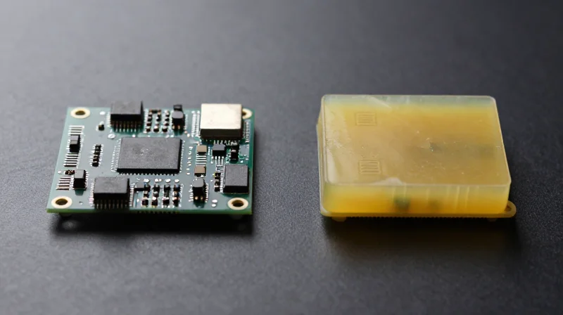
Performance Benchmarking: Coatings vs. Potting
Selecting the optimal protection strategy requires balancing the lightweight, conformal nature of advanced coatings against the robust, volumetric encapsulation provided by potting compounds. While conformal coatings offer superior weight efficiency and accessibility for rework, potting compounds excel in extreme environments where structural integrity, vibration damping, and total chemical isolation are mandatory.
| Feature | Conformal Coatings | Potting Compounds |
|---|---|---|
| Weight Impact | Negligible | Significant |
| Thermal Management | Passive/Convection | Conductive/Thermal Mass |
| Repairability | High | Low to Impossible |
| Environmental Seal | Barrier/Resistance | Hermetic/Total Block |
| Application Speed | High (Automated) | Low (Curing time/Volume) |
Lifecycle and Reliability Considerations
The lifecycle efficacy of these materials is dictated by the Coefficient of Thermal Expansion (CTE). Mismatched CTEs between rigid potting compounds and sensitive surface-mount components can lead to solder joint fatigue over thermal cycling. Conversely, advanced thin-film coatings minimize stress, extending the MTBF (Mean Time Between Failures) for densely packed, high-frequency circuits.
- Does potting increase total unit weight?
Yes, potting compounds significantly add mass, which can be a critical constraint in aerospace and portable device applications. - Which material offers better protection against high-pressure wash?
Potting provides a superior, non-porous physical barrier compared to thin-film coatings, ensuring absolute liquid exclusion. - How does thermal cycling affect long-term reliability?
Rigid potting can create mechanical stress during cycling, whereas elastic conformal coatings allow for material expansion without fracturing components. - Is reworkability essential for your lifecycle strategy?
If PCBs require component replacement or diagnostic access, conformal coatings are the preferred choice as they are easier to remove or penetrate.
Design Considerations for Miniaturized Hardware
Optimizing Board Layout for Advanced Protection
In miniaturized systems, the mechanical boundaries of the PCB are tighter than ever. Engineers must transition from 'after-the-fact' protection planning to 'design-for-protection' workflows. This involves balancing component density with the fluid dynamics of coating materials, ensuring that low-viscosity solutions do not wick into forbidden areas like high-precision connectors or optical sensors.
Clearance and Zoning Strategy
| Design Element | Conformal Coating Impact | Potting Compound Impact |
|---|---|---|
| Keep-out Zones | Minimal; allows for tight spacing | High; requires significant edge margins |
| Component Height | Accommodates low-profile SMT | Adds significant weight and volume |
| Thermal Management | Excellent heat dissipation | Acts as a thermal insulator |
| Ease of Inspection | Visual/UV light verification | Requires X-ray or destructive testing |
Inspection and Rework Considerations
Miniaturization complicates inspection due to high component density and masked solder joints. Integrating UV-traceable dyes into the coating process is no longer optional for high-reliability hardware; it is essential for automated optical inspection (AOI). Furthermore, designers should define 'no-coat' zones early in the EDA environment to ensure that critical rework paths remain accessible for potential field repairs.
Frequently Asked Questions
- How does miniaturization affect the choice between Parylene and liquid coatings?
Parylene's vapor-phase deposition is superior for ultra-miniature geometries where liquid wicking poses a risk to connectors; however, it requires specialized vacuum equipment and longer cycle times. - What is the primary risk when using potting compounds on small boards?
Coefficient of Thermal Expansion (CTE) mismatch is critical. On small, dense boards, potting compounds can exert mechanical stress on delicate solder joints during thermal cycling, leading to fractured connections. - Can I simplify inspection in high-density layouts?
Yes, by utilizing laser-direct masking or stencil-based coating application, you can ensure precise material coverage, which reduces the need for complex multi-angle inspection.
Cost-Benefit Analysis for Manufacturing at Scale
Evaluating Total Cost of Ownership in PCB Protection
Achieving manufacturing scale requires moving beyond simple per-unit material costs to evaluate the Total Cost of Ownership (TCO). While potting compounds often present lower raw material prices, advanced conformal coatings—particularly UV-cure chemistries—frequently offer a superior return on investment through significant reductions in cycle time, footprint, and rework rates.
| Cost Driver | Conformal Coating (Automated) | Traditional Potting |
|---|---|---|
| Material Consumption | Low (Micron-level thickness) | High (Volume filling) |
| Process Cycle Time | Fast (Seconds to minutes) | Slow (Extended cure cycles) |
| Capital Investment | Moderate (Robotic dispensers) | High (Mixing/metering systems) |
| Inspection/Rework | Accessible/Reversible | Difficult/Destructive |
Key Economic Drivers for High-Volume Scaling
- Does material volume significantly impact the bottom line?
Yes, potting compounds require substantial volumes to fill housings, adding weight and cost. Conformal coatings minimize weight and material usage, yielding higher margins in high-volume production. - How does curing time affect throughput?
Potting often requires hours to cure, creating a major production bottleneck. UV-curable conformal coatings enable near-instant curing, allowing for immediate inline testing and packaging. - What is the hidden cost of rework?
Potting compounds are typically permanent; failed boards often result in total scrappage. Conformal coatings can be removed or patched, offering a substantial insurance policy against high-value assembly losses.
Engineers must also account for the cost of floor space. Automated conformal coating lines are modular and compact, whereas potting operations often require extensive curing ovens or expansive staging areas, increasing overhead costs per square foot in modern manufacturing facilities.
Making the Final Selection
A Strategic Framework for Decision-Making
The final selection between conformal coatings and potting compounds should be treated as a balancing act between physical robustness and lifecycle maintainability. Engineers must move beyond initial material costs and evaluate the total cost of ownership (TCO) alongside the specific performance requirements of the end-use environment.
| Requirement | Recommended Strategy | Primary Justification |
|---|---|---|
| High-Shock/Vibration | Potting Compounds | Superior mechanical damping and structural support |
| Field Repairability | Conformal Coatings | Easy removal and localized rework accessibility |
| Rapid Assembly | Conformal Coatings | Lower cycle times and automated selective application |
| Extreme Submersion | Potting Compounds | Total encapsulation creates a superior barrier to moisture |
Key Evaluation Criteria
- How does weight sensitivity influence the choice?
Potting compounds significantly increase the mass of the PCB, which is often disqualifying for aerospace or portable electronics; in such cases, thin-film coatings are mandatory. - Is thermal management a deciding factor?
Yes. While potting can act as a heat sink, it also traps heat around high-power components; choose thermally conductive potting if heat dissipation is a primary failure mode. - What role does inspectability play?
Conformal coatings allow for visual and optical inspection post-application, whereas potting compounds require X-ray analysis to verify the integrity of the protection layer.
To finalize your strategy, categorize your product into 'High-Reliability/Fixed-Installation' or 'Mobile/Consumer-Grade'. For fixed assets in harsh environments, the uncompromising moisture and shock protection of potting outweighs the weight penalty. Conversely, for competitive markets requiring rapid iteration and repair, advanced conformal coatings provide the necessary flexibility to keep your production line lean and your products serviceable.
Selecting the right protection strategy is no longer just about environmental shielding; it is about balancing performance, weight, and manufacturing efficiency. By moving beyond legacy potting toward advanced deposition and UV-cure solutions, you ensure your hardware remains competitive in an increasingly demanding market. Ready to optimize your hardware’s durability? Contact our engineering team today for a custom consultation on your current design requirements.
