
As the global transition to electrification accelerates, power density has become the new frontier for hardware engineers. Managing high currents within shrinking form factors is no longer just a design challenge—it is a competitive necessity. This article explores how industry leaders are balancing the reliability of traditional heavy copper PCBs with the structural efficiency of emerging busbar integration strategies.
The Power Density Dilemma
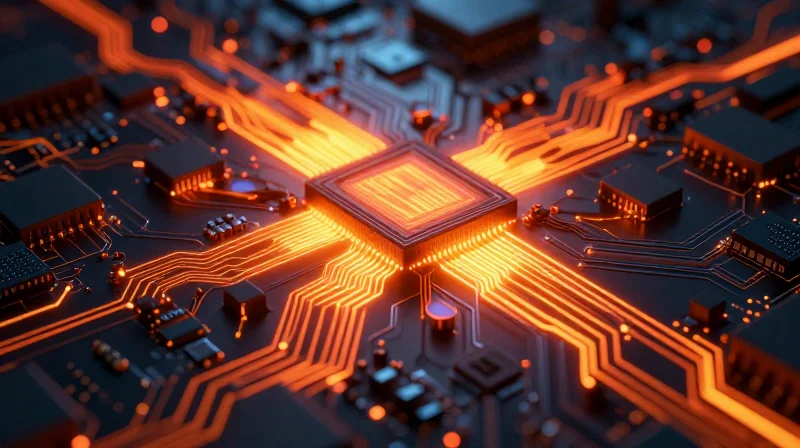
Thermal Limits of High-Density Circuits
As power electronics evolve, the demand for increased current capacity within shrinking physical footprints has created a bottleneck in thermal dissipation. The fundamental challenge is that traditional substrate designs struggle to conduct heat away from switching components efficiently, leading to potential thermal runaway. In high-performance electric vehicle (EV) inverters and industrial motor controllers, the concentration of massive current through increasingly narrow conductive paths converts electrical resistance into heat at an unsustainable rate.
Conductivity Challenges in Compact Assemblies
Engineers face a rigid constraint: the Joule heating effect ($P = I^2R$). When you increase current density to meet performance requirements, you must either reduce electrical resistance—via thicker conductors or superior materials—or drastically improve the heat transfer coefficient of the assembly. Thick copper PCBs have long served as the industry standard, but they are approaching physical limits where the mechanical stress of thermal expansion threatens interconnect reliability.
| Challenge | Impact on Performance | Design Constraint |
|---|---|---|
| Current Density | Accelerated component aging | Cross-sectional area |
| Thermal Impedance | Reduced efficiency | Substrate thermal conductivity |
| Mechanical Stress | Interconnect failure | CTE mismatch |
- Why is heat dissipation the primary hurdle?
As power density increases, the heat generated per square millimeter exceeds the cooling capacity of standard PCB substrates, leading to localized hotspots that shorten device lifespan. - How do busbars differ from thick copper PCBs?
Busbars offer superior bulk cross-sectional area for current flow and improved structural rigidity, often enabling better passive or active cooling compared to laminar PCB structures. - What dictates the transition point for new technologies?
Transition usually occurs when current requirements exceed 100A, where the weight and thermal resistance of copper-clad laminates become inefficient compared to dedicated copper or aluminum busbar solutions.
Anatomy of Thick Copper PCBs
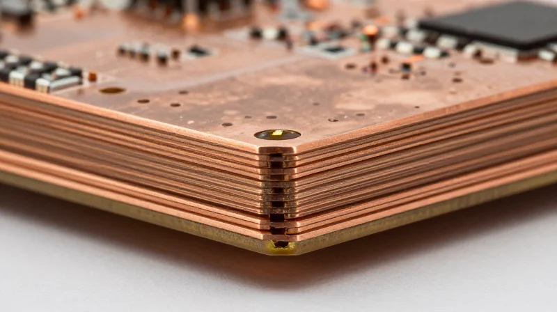
Engineering Principles of Heavy Copper Design
Thick copper PCBs, often referred to as heavy copper boards, utilize outer and inner layers with copper weights typically ranging from 3 oz/ft² (105 µm) up to 20 oz/ft² (700 µm) or more. Unlike standard 1 oz/ft² boards, these substrates are engineered specifically to minimize resistive losses—a critical requirement for high-power applications. By increasing the cross-sectional area of the conductive traces, designers can maintain a lower temperature rise under high current loads, effectively mitigating the risk of thermal failure and signal degradation.
Fabrication and Performance Characteristics
| Feature | Standard PCB (1 oz) | Thick Copper PCB (3 oz+) |
|---|---|---|
| Current Capacity | Low/Moderate | High/Extreme |
| Thermal Conductivity | Limited | Excellent (Heat Spreading) |
| Fabrication Complexity | Standard | High (Etch Compensation) |
| Mechanical Rigidity | Standard | High |
The fabrication process for thick copper demands specialized manufacturing techniques. As copper thickness increases, standard chemical etching requires significant compensation to account for undercutting, where the etchant removes copper from the sides of traces, potentially creating trapezoidal profiles. Furthermore, the lamination process for multi-layer heavy copper requires high-flow prepregs to fill the large gaps between thick traces, ensuring structural integrity and preventing delamination under extreme thermal cycling.
Critical Reliability Benefits
- How does thickness affect thermal dissipation?
The increased bulk copper acts as an integrated heat sink, efficiently spreading localized heat from power components like MOSFETs or IGBTs across a larger PCB area, reducing hotspots. - What is the primary advantage for high-current loops?
It significantly reduces ohmic resistance (I²R losses), allowing for higher power throughput with less energy waste and reduced thermal stress on board-level components. - Can these boards survive mechanical stress?
Yes, the thicker copper layers increase the overall board stiffness, which enhances vibration resistance—a critical factor for automotive and industrial machinery environments.
The Rise of Integrated Busbar Systems
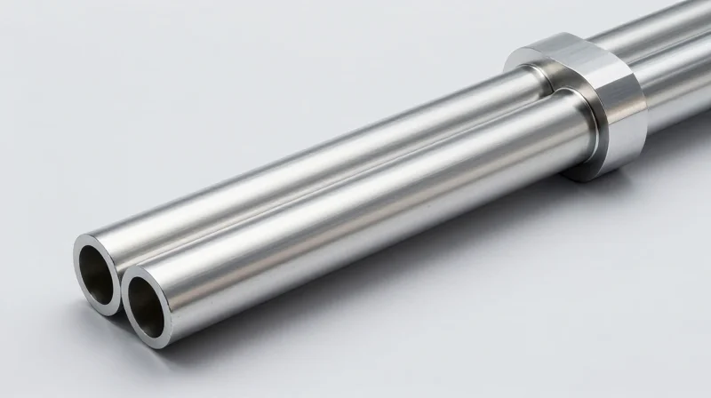
As the demand for extreme power density in electric vehicle (EV) powertrains and industrial drives continues to escalate, traditional printed circuit boards—even those utilizing heavy copper layers—are reaching physical thermal and conductive limitations. Integrated busbar systems address these bottlenecks by utilizing rigid, high-conductivity metal structures that provide superior current-carrying capacity, reduced parasitic inductance, and significantly improved thermal management compared to laminate-based solutions.
Core Advantages of Busbar Integration
The transition from PCB-based power distribution to integrated busbar assemblies allows for a radical simplification of power architecture. By shifting the primary current-carrying burden from thin copper traces to solid, multi-layer metal bars, designers can achieve lower contact resistance and eliminate the thermal degradation issues common to substrate-bonded copper.
| Feature | Thick Copper PCB | Integrated Busbar System |
|---|---|---|
| Current Density | Moderate | Very High |
| Inductance | Higher | Low/Optimized |
| Thermal Mass | Low | High |
| Assembly Complexity | Standard | High Precision |
Frequently Asked Questions
- When should an engineer opt for busbars over PCBs?
Busbars are preferable when the current requirements exceed the thermal or physical limits of a 3oz to 6oz copper PCB, typically in high-voltage traction inverters or grid-scale energy storage. - Do busbars increase system footprint?
While busbars occupy volume, their high current-carrying capacity allows for a smaller overall system footprint by eliminating the need for large banks of parallel PCB traces and complex thermal relief vias. - How is reliability affected by vibration?
Integrated busbar systems, when properly supported, provide superior structural integrity, reducing the risk of fatigue-related fractures that can affect brittle solder joints on high-mass PCB components.
Comparative Analysis: Electrical Performance and Impedance
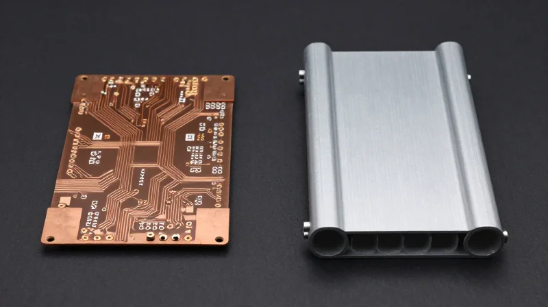
The choice between thick copper PCBs and busbars is fundamentally a trade-off between the design flexibility of planar integration and the raw performance metrics of volumetric conductors. While thick copper PCBs have advanced significantly, they remain limited by trace length and skin effect concerns at high frequencies, whereas busbars offer superior cross-sectional area and thermal mass for high-current power distribution.
Comparative Electrical Metrics
| Parameter | Thick Copper PCB | Integrated Busbar |
|---|---|---|
| Current Density | Moderate (I2R limit) | High (Thermal mass dominant) |
| Parasitic Inductance | Low (but trace-dependent) | Ultra-low (geometrically optimized) |
| Voltage Drop | Higher due to path length | Minimal (low DC resistance) |
| Thermal Dissipation | Board-level via conduction | Direct ambient/chassis cooling |
Parasitics and Impedance Management
In high-speed switching environments, such as SiC-based traction inverters, parasitic inductance is the primary driver of voltage overshoot. Thick copper PCBs often suffer from magnetic flux paths constrained by board layers. Conversely, laminated busbars utilize close-proximity stacking of positive and negative layers, which allows for electromagnetic cancellation, significantly reducing loop inductance and improving overall EMI performance.
Performance FAQ
- At what current threshold do busbars outperform thick copper PCBs?
Busbars become the superior choice when total current loads exceed 150-200A continuously, where the copper weight required on a PCB leads to unsustainable board thickness and manufacturing complexity. - How does skin effect influence these conductors?
Both suffer from skin effect at high frequencies, but the large flat surface area of busbars can be optimized with skin-effect-mitigating geometries, whereas PCB traces are constrained by the rigid dielectric structure. - Can hybrid approaches offer a middle ground?
Yes, many modern designs utilize 'PCB-embedded busbars' or heavy-duty solder-on power plates that bridge the gap, providing busbar-like current capacity while maintaining PCB-style assembly automation.
Thermal Management Trade-offs
Thermal management in high-power electronics is defined by the efficiency of the heat dissipation path from the source to the ambient environment. While thick copper PCBs integrate thermal management directly into the substrate, they remain constrained by the thermal conductivity of the PCB material itself. Conversely, busbars act as dedicated heat sinks that decouple high-current thermal loads from sensitive substrate materials.
Heat Dissipation Pathways
Thick copper PCBs rely on copper's high thermal conductivity to spread heat laterally across the board surface, often utilizing thermal vias to move heat to internal layers or the backside. However, as power levels exceed standard PCB cooling limits, the dielectric material creates a thermal bottleneck. Busbars, by contrast, offer a high-mass metallic path that can be directly coupled to external cooling solutions, effectively bypassing the PCB's thermal resistance entirely.
| Feature | Thick Copper PCB | Integrated Busbar System |
|---|---|---|
| Primary Thermal Path | Lateral spreading via copper layers | Direct conduction through rigid metal |
| Substrate Sensitivity | High (subject to localized hotspots) | Low (load decoupled from substrate) |
| Cooling Interface | Thermal vias/heatsinks on board | Direct attachment/busbar surface |
| Thermal Mass | Limited by board thickness | High (proportional to busbar cross-section) |
Impact on Component Reliability
Elevated temperatures accelerate component degradation, particularly for capacitors and semiconductors sensitive to thermal cycling. Thick copper PCBs often suffer from uneven thermal distribution, where concentrated current paths create localized hotspots that degrade nearby dielectric materials. Busbars mitigate this risk by acting as an extension of the lead frame, ensuring that the high heat generated by current transmission does not saturate the board-level environment.
Frequently Asked Questions
- Does a busbar always offer better thermal performance than a thick copper PCB?
Not necessarily; while busbars offer superior bulk thermal capacity, they require significant mechanical space. Thick copper PCBs remain more efficient for compact designs where heat can be effectively managed through strategic via placement. - How does the choice between busbars and PCBs affect thermal cycling stress?
Busbars generally experience higher mechanical stress due to thermal expansion differentials between the metal and the chassis, whereas thick copper PCBs are prone to thermal fatigue at solder joint interfaces.
Cost, Scalability, and Manufacturing Complexity
The choice between thick copper PCBs and busbar systems hinges on a balance between assembly integration and raw material costs. While thick copper PCBs offer seamless integration with surface-mount technology (SMT) and lower initial setup costs for low-to-mid volume production, busbar systems provide superior economic scaling for high-current applications by reducing board complexity and minimizing material waste.
Cost and Scalability Matrix
| Metric | Thick Copper PCB | Busbar System |
|---|---|---|
| Unit Cost (Low Volume) | Moderate | High |
| Unit Cost (Mass Production) | High (Material dependent) | Low (Standardized stampings) |
| Tooling Complexity | Low | High (Die-cast/Bending) |
| Assembly Speed | High (SMT automation) | Moderate (Manual/Robotic fastening) |
Manufacturing Complexity Considerations
Thick copper PCBs (exceeding 3oz or 105µm) introduce significant manufacturing constraints. Etching thick copper requires precise control over side-wall profile and trace width to prevent undercutting, which limits density. In contrast, busbar manufacturing shifts complexity from photolithography to mechanical engineering—involving precision stamping, bending, and insulation coating. Busbars often require additional assembly steps, such as press-fit connections or high-current fasteners, which can increase the total assembly footprint compared to a singular PCB-based solution.
Frequently Asked Questions
- Which technology is better for rapid prototyping?
Thick copper PCBs are generally superior for prototyping because they integrate with standard PCB design flows and do not require custom mechanical tooling like busbars do. - Does busbar implementation reduce assembly time?
Not necessarily; while busbars remove current-carrying stress from the PCB, the mechanical fastening of busbars to components often adds manual labor time that SMT reflow processes avoid. - How does material waste influence scalability?
In mass production, copper PCBs experience high scrap rates during the deep etching of thick layers. Busbars, typically formed via stamping, offer higher material efficiency as the copper is shaped rather than chemically removed.
The Hybrid Architecture Future
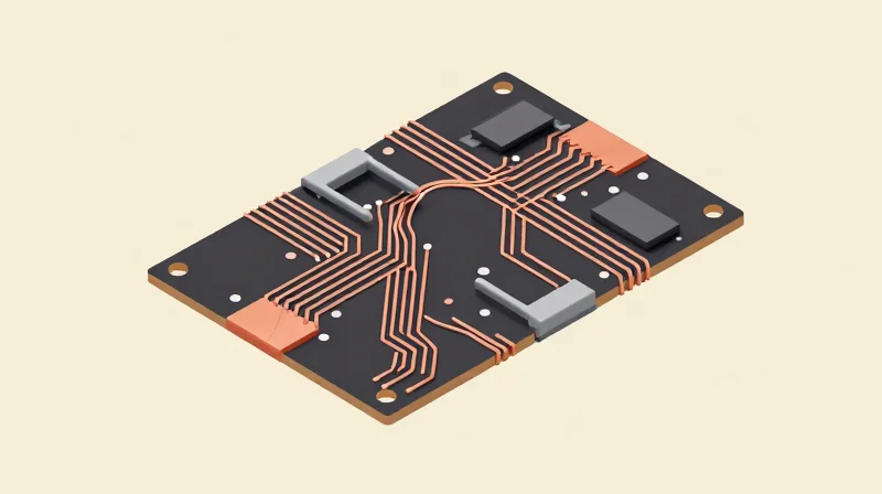
The Convergence of PCB and Busbar Technologies
The future of power electronics is not a choice between thick copper PCBs and busbars, but rather a strategic convergence of both. Designers are increasingly adopting a modular hybrid approach where high-density signal logic is handled by heavy copper PCBs, while massive power distribution paths are offloaded to structural busbars. This symbiotic relationship mitigates the thermal limitations of traditional board-level copper while preserving the compact, automated assembly benefits of PCBs.
Key Advantages of Hybrid Integration
- Optimized Current Density
Utilizes busbars for primary high-current rails to reduce board stress and hot spots, leaving the PCB to manage complex gate drive and feedback circuitry. - Enhanced Mechanical Integrity
Structural busbars act as a mechanical backbone, reducing board flexing and vibration-induced fatigue common in heavy, large-format PCB assemblies. - Scalable Manufacturing
Allows for standardized PCB sub-assemblies to be paired with application-specific busbar configurations, reducing total product development cycles.
Comparative Performance Metrics
| Feature | Thick Copper PCB | Hybrid Integration | Busbar System |
|---|---|---|---|
| Current Handling | Moderate | High | Extreme |
| Signal Logic | Excellent | Excellent | Poor |
| Automation Ease | High | High | Moderate |
| Space Efficiency | High | Moderate | Low |
Future Outlook and Implementation Strategy
Moving forward, the successful implementation of hybrid architectures will rely on advanced interconnects—specifically, solder-free press-fit pins and custom busbar mounting hardware. These solutions minimize contact resistance and streamline production, allowing designers to bypass the limitations of traditional solder joints in high-temperature applications. As electric vehicle and renewable energy demands rise, this tiered approach—separating the 'brain' of the power electronics from the 'muscle' of the distribution system—will define the next generation of power system architecture.
Selecting the Right Solution for Your Application
The choice between thick copper PCBs and busbars is no longer a binary decision but a strategic trade-off centered on power density and system integration. Engineers must prioritize current handling capacity, structural stiffness, and assembly automation when evaluating these technologies for high-performance power stages.
Decision Matrix: Thick Copper PCB vs. Busbar Alternatives
| Requirement Factor | Thick Copper PCB | Busbar System |
|---|---|---|
| Current Density | Moderate (High trace resistance) | Superior (Low resistive loss) |
| Component Density | High (Supports integrated control) | Low (Power stage dedicated) |
| Mechanical Rigidity | Low (Requires external mounting) | High (Self-supporting) |
| Assembly Speed | Automated/Standard SMT | Manual or Robotic bolting |
When to Choose Thick Copper PCBs
Thick copper PCBs (typically >3 oz copper) are the ideal choice when your design requires high integration of logic, control, and gate drive circuitry alongside power delivery. They excel in compact designs where the power stage consumes less than 100A, allowing for a single-board solution that eliminates complex interconnects.
When to Transition to Busbars
Busbar integration becomes mandatory when your architecture transitions into high-current environments—typically exceeding 150A. By moving the high-current path off the PCB, you reduce the thermal stress on expensive FR4 substrate materials and improve reliability through enhanced parasitic inductance management.
Engineering FAQ
- Can I mix these technologies?
Yes. Most modern high-power systems utilize a hybrid approach, using thick copper PCBs for local switching loops and busbars for bulk DC link distribution. - Which offers better EMI performance?
Busbars generally offer superior EMI performance for high-current paths due to lower loop inductance, whereas PCBs are better for managing high-frequency signal noise. - Does the board material limit copper thickness?
Extreme copper weights often require specialized high-Tg (glass transition temperature) laminates to prevent delamination during the extended heat cycles required for soldering heavy copper.
Whether you are optimizing for weight, thermal efficiency, or manufacturing throughput, the choice between thick copper PCBs and busbar integration will define your product's performance. As the industry evolves, finding the right hybrid approach is essential for scaling power electronics reliably. Contact our engineering team today to discuss your power distribution requirements and build a more efficient, future-proof design.
