
As data centers face unprecedented demand for speed, the physical foundation of server performance—the PCB—is undergoing a radical transformation. Moving beyond legacy constraints, we explore how cutting-edge board architectures are enabling the next wave of high-frequency infrastructure.
The Shifting Landscape of Server Demand
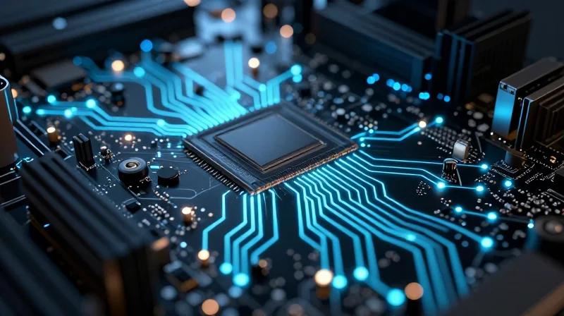
The architecture of modern server hardware is undergoing a seismic shift driven by the insatiable demands of generative AI, real-time analytics, and massive-scale cloud computing. These workloads require unprecedented bandwidth and power density, forcing engineers to move beyond conventional design methodologies. As signal frequencies increase and latency requirements tighten, the motherboard is no longer just a passive interconnect; it is a critical bottleneck that must be re-engineered through advanced high-layer PCB technologies.
Drivers of Architectural Strain
The convergence of three primary trends is creating an environment where traditional PCB designs fail to keep pace with performance requirements.
- AI and Accelerated Computing
The transition toward high-density GPU clusters requires extreme power delivery and massive signal integrity throughput to avoid thermal throttling and packet loss. - Data Center Convergence
The move toward hyper-converged infrastructure demands higher layer counts to accommodate complex high-speed bus architectures and increased I/O density within standard chassis footprints. - Edge Intelligence
Deploying analytics at the edge necessitates extreme signal reliability despite volatile environmental conditions, pushing the limits of current dielectric material performance.
Physical Limits of Conventional PCB Design
| Constraint Factor | Legacy Limitation | Emerging Requirement |
|---|---|---|
| Signal Frequency | Below 28 Gbps | Above 112 Gbps |
| Layer Density | 10-14 Layers | 20+ Layers |
| Dielectric Loss | Standard FR-4 | Ultra-low Loss Laminates |
To support 112 Gbps (and eventually 224 Gbps) per channel, the industry is forced to adopt materials with lower dielectric constants (Dk) and dissipation factors (Df). However, these materials introduce significant manufacturing challenges, including increased vulnerability to thermal expansion (CTE) mismatches and potential copper-roughness-related signal attenuation. Consequently, the future of server hardware resides at the intersection of high-layer-count board fabrication and the precise management of high-frequency signal propagation.
Limitations of Legacy PCB Manufacturing
The Physical Limits of Traditional Fabrication
Traditional PCB manufacturing processes, primarily based on subtractive etching and standard lamination, are hitting a wall as server hardware requirements shift toward extreme miniaturization and high-frequency data transmission. These legacy methods introduce inherent physical constraints that compromise performance in high-speed, high-density environments.
Critical Performance Bottlenecks
| Constraint | Impact on Performance | Legacy Limitation |
|---|---|---|
| Signal Integrity | Increased insertion loss and crosstalk | Copper surface roughness at high frequencies |
| Thermal Management | Localized hotspots and thermal stress | Low thermal conductivity of standard substrates |
| Manufacturing Precision | Reduced routing density | Limitations in via-in-pad and micro-via scaling |
Thermal and Signal Integrity Challenges
In contemporary server designs, the proliferation of AI and GPU clusters mandates unprecedented power densities. Legacy multi-layer boards often struggle to dissipate heat efficiently due to the low thermal conductivity of glass-reinforced epoxy laminates. Furthermore, as data speeds exceed 56Gbps and approach 112Gbps/224Gbps per lane, the skin effect and dielectric loss become catastrophic. The standard subtractive processes used to create traces leave uneven edges, leading to significant signal degradation that advanced architectures can no longer tolerate.
Frequently Asked Questions
- Why does copper roughness affect high-speed signals?
At high frequencies, the 'skin effect' causes current to flow primarily on the surface of the conductor. If the copper surface is rough, the effective path length increases and impedance stability is lost, leading to increased signal loss. - How does layer count impact reliability in legacy processes?
As layer counts increase, the accumulation of mechanical stress during thermal cycling can lead to via barrel cracking and delamination, as traditional bonding materials are not optimized for extreme dimensional stability. - Is standard lamination sufficient for 800G networking?
No, standard lamination materials often possess high dissipation factors that inhibit the signal integrity required for 800G and beyond, necessitating a shift toward advanced low-loss dielectric materials.
Advanced Materials and High-Layer Count Solutions
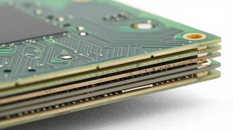
Advanced Materials and High-Layer Count Solutions
To support the extreme data rates required by modern AI and cloud infrastructures, server manufacturers are moving toward ultra-low-loss dielectric materials and high-density interconnect (HDI) designs. These advanced solutions are essential to combat signal attenuation, crosstalk, and thermal constraints that plague legacy multi-layer boards.
Material Science: The Shift to Ultra-Low Loss
The transition to 400G and 800G Ethernet necessitates substrates with ultra-low dissipation factors (Df). By replacing standard FR-4 epoxies with modified polyphenylene ether (mPPE) or advanced PTFE-based laminates, designers can drastically reduce dielectric absorption and signal loss. These materials ensure that high-frequency electromagnetic waves remain stable even across long, complex signal paths within a high-layer count board.
| Material Type | Loss Characteristic | Primary Application |
|---|---|---|
| Standard FR-4 | High | Low-speed legacy systems |
| High-Tg/Mid-Loss | Moderate | Standard server backplanes |
| Ultra-Low Loss (mPPE) | Very Low | 800G switches & AI training |
| PTFE-Based | Extremely Low | RF/Microwave & high-frequency logic |
High-Layer Count Architectures and HDI
Modern server boards often exceed 20 to 30 layers to accommodate increased component density and complex power delivery networks. Implementing 'Any-Layer' HDI (High-Density Interconnect) technology allows for microvias and staggered via configurations that minimize signal stubs. These stubs typically act as antennas that cause resonance and reflection in high-speed circuits, and their mitigation is critical for maintaining signal integrity in dense board layouts.
- Why is layer count increasing?
Higher layer counts provide the necessary surface area for complex routing and robust power planes, preventing voltage drops while isolating high-speed data lanes. - What role do microvias play?
Microvias reduce the size of signal vias, decreasing parasitic capacitance and inductance, which allows for cleaner signal propagation at higher frequencies. - How do these designs manage thermal load?
Increased internal copper mass and thermally conductive prepregs help distribute heat away from localized GPU/CPU hotspots, protecting sensitive signal paths from thermal degradation.
Signal Integrity in High-Frequency Environments

Challenges of Signal Integrity at PCIe 5.0+ Speeds
As data rates accelerate into the 32 GT/s and 64 GT/s domain, the physical PCB environment behaves less like a standard circuit and more like a high-frequency waveguide. Signal integrity degradation, primarily manifested through insertion loss, crosstalk, and impedance discontinuities, becomes the primary bottleneck for system reliability. Managing these phenomena necessitates a departure from standard manufacturing tolerances toward a holistic design-for-manufacturing (DFM) philosophy.
Critical Mitigation Strategies
- Advanced Dielectric Selection
Utilizing ultra-low-loss (ULL) laminates with stable dielectric constants (Dk) and ultra-low dissipation factors (Df) minimizes signal attenuation across wider frequency bands. - Impedance Discontinuity Reduction
Implementing back-drilling techniques for plated through-hole (PTH) vias is essential to remove parasitic stubs that cause significant signal reflection at high frequencies. - Crosstalk Minimization
Adopting aggressive routing topologies, such as differential pair spacing optimization and increased reference plane coupling, reduces electromagnetic coupling between adjacent high-speed lanes.
Comparison of Design Approaches
| Design Strategy | Primary Impact | Complexity Level |
|---|---|---|
| Back-drilling Stubs | Eliminates resonance | High |
| Broadside Coupling | Improves density | Extreme |
| Low-Dk Laminates | Reduces signal loss | Moderate |
| Surface Roughness Reduction | Minimizes skin effect | Moderate |
The Role of Electromagnetic Simulation
The margin for error in high-frequency server design is nearly non-existent. Engineers must employ full-wave 3D electromagnetic solvers to analyze the entire signal path—from the silicon bump to the connector pin. This simulation-driven workflow allows for the iterative refinement of trace geometries and via transitions, ensuring that signal integrity is verified long before physical fabrication commences. In the era of PCIe 6.0, simulation is no longer optional; it is the fundamental bridge between theoretical architecture and functional hardware.
Thermal Management and Power Delivery Innovations
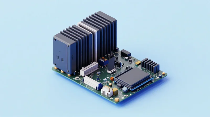
Thermal Management Through PCB Substrate Integration
As TDPs for CPUs and GPUs exceed 500W, traditional heat sinking is no longer sufficient. Modern high-layer PCB designs now integrate embedded copper coins and micro-via thermal cooling paths directly into the substrate. By replacing standard dielectric materials with advanced thermal-conductive resins near high-power components, engineers can effectively route heat away from hotspots, reducing the thermal stress on critical signal vias and copper traces.
Optimizing Power Delivery Networks (PDN)
Minimizing voltage droop and electromagnetic interference requires a robust PDN. Emerging industry trends favor vertical power delivery, which utilizes the underside of the PCB to place voltage regulator modules closer to the processor. This architecture significantly reduces ohmic losses and ensures cleaner signal integrity under high-load conditions.
| Feature | Legacy Approach | Modern Innovation |
|---|---|---|
| Heat Dissipation | External Heatsinks | Embedded Copper Vias & Coins |
| Power Routing | Lateral PCB Traces | Vertical Power Delivery (VPD) |
| Material Use | Standard FR-4 | High-Tg Thermal Resins |
Frequently Asked Questions
- How do embedded copper coins improve server reliability?
Copper coins provide a direct, high-thermal-conductivity path from the chip package to the PCB surface, preventing the localized overheating that often leads to solder joint fatigue. - What is the primary benefit of Vertical Power Delivery?
VPD reduces the physical distance between power regulators and processors, which minimizes parasitic inductance and resistance, resulting in significantly more efficient power conversion at the silicon level.
The Rise of Optical Interconnects and Integrated Photonics
Transitioning from Copper to Light
As data rates move beyond 112G and 224G SerDes, traditional copper traces face the 'brick wall' of insertion loss, forcing architects to look toward board-level optical interconnects. By integrating photonics directly onto the PCB or within the package, servers can achieve near-zero latency and massive throughput scaling that copper simply cannot sustain over mid-to-long-range board distances.
Comparative Analysis: Copper vs. Optical
| Metric | Traditional Copper | Optical Interconnects |
|---|---|---|
| Bandwidth Scaling | Limited by Skin Effect | Virtually Unlimited |
| Signal Loss | High (increases with length) | Very Low |
| Power Efficiency | Degrades at High Frequencies | Constant across distances |
| Manufacturing Complexity | Mature/Standard | High/Emerging |
Key Advantages of Photonic Integration
- Thermal Management
Optical signals generate significantly less heat than high-power copper drivers, reducing the thermal load on the PCB and enabling denser component placement. - Reduced EMI
Photonic signals are immune to electromagnetic interference, eliminating the need for complex shielding and crosstalk mitigation strategies required by copper traces. - Density Optimization
Optical fibers take up less physical space than bulky high-speed copper cabling, allowing for improved airflow and higher rack-level component density.
Challenges and Future Outlook
Despite the performance gains, integrating silicon photonics requires significant changes to the server manufacturing ecosystem. Reliability of laser sources, the precision of fiber coupling, and cost-effective packaging remain the primary barriers to mass adoption. However, as AI and machine learning workloads demand ever-increasing throughput, industry efforts in co-packaged optics (CPO) are quickly closing the gap between research and commercial deployment.
Manufacturing Challenges and Quality Control
The Precision-Complexity Trade-off
As server boards evolve toward higher layer counts—often exceeding 20 or 30 layers—the manufacturing process faces severe constraints. Increased layer density necessitates finer line widths and narrower spacing, which directly increases the risk of registration errors and internal delamination. Manufacturers must adopt advanced semi-additive processes (SAP) to maintain electrical performance, but these techniques inherently raise production costs and extend cycle times. Balancing these high-precision requirements with the need for high-volume throughput remains the single largest bottleneck in server infrastructure deployment.
Comparative Reliability Metrics
| Manufacturing Variable | High-Layer Impact | Quality Control Strategy |
|---|---|---|
| Registration Accuracy | Increased risk of via misalignment | Automated Optical Inspection (AOI) with X-ray drilling |
| Dielectric Thickness | High signal loss/Crosstalk | Impedance TDR testing at production line |
| Surface Finish | Solder joint fragility | Periodic SEM cross-sectional analysis |
Ensuring 24/7 Enterprise Reliability
For enterprise environments, the 'fit-and-forget' nature of server hardware demands near-zero defect rates. Quality control has transitioned from post-production sampling to in-situ monitoring of the lamination cycle. By utilizing real-time feedback loops during the heat-press phase, manufacturers can now mitigate potential warping and glass-weave effects that compromise signal integrity over time.
- How does layer count impact failure rates?
Increased layer counts complicate the thermal expansion coefficients of the substrate, making boards more susceptible to micro-crack propagation under constant thermal cycling. - What is the role of AOI in modern fabrication?
Automated Optical Inspection is now critical for verifying internal circuit geometries that are physically impossible to inspect manually, ensuring continuity in high-density interconnects. - Is cost-reduction compromising board integrity?
While there is pressure to reduce costs, cutting corners on laminate materials or resin content often leads to premature field failure, which far outweighs initial manufacturing savings.
Future-Proofing Your Infrastructure Strategy
Anticipating Technological Obsolescence
To remain competitive, IT decision-makers must treat PCB architecture not as a static component, but as the foundational substrate for upcoming modular compute architectures. As processor TDPs continue to climb, hardware strategies must shift from rigid, monolithic board designs toward agile architectures that support rapid upgrades in interconnect standards, such as CXL (Compute Express Link), without requiring a complete chassis overhaul.
Comparison of Infrastructure Strategies
| Strategy | PCB Focus | Scalability Potential | Long-term Cost Efficiency |
|---|---|---|---|
| Standard Copper Routing | Conventional High-Layer Count | Low (Bottlenecked by EMI) | Low (Limited lifespan) |
| Optical-Ready Substrates | Embedded Waveguides/Signal Layers | High (Supports future speeds) | High (Investment longevity) |
| Modular Blade Integration | Advanced Thermal/Power Planes | Moderate (Physical constraints) | Moderate (High initial CapEx) |
Key Considerations for Decision-Makers
- How do I balance immediate budget constraints with long-term infrastructure needs?
Prioritize PCB platforms that utilize open-standard mechanical form factors and high-layer counts capable of supporting future signal bandwidths, even if they appear over-specified today. - Why is signal integrity becoming a critical purchase metric?
As data rates reach 112G and 224G PAM4, the physical quality of the PCB layers determines the maximum achievable throughput; choosing boards with advanced low-loss dielectric materials prevents future performance ceilings. - Will optical integration replace my current copper-based infrastructure?
Optical integration is accelerating for inter-rack and board-to-board communication; selecting hardware designed with 'optical-ready' PCB routing paths ensures a smoother transition as photonics becomes standard.
The transition to next-generation PCB architectures is no longer optional for organizations scaling their digital presence. By prioritizing high-performance board design, businesses can ensure their infrastructure remains robust against rising frequency demands. Contact our engineering team today to audit your current hardware roadmap and prepare for the future of enterprise computing.
