
As global energy demands surge, the limitations of traditional silicon-based power systems are hitting a wall. Engineers now face a critical pivot point: stick to proven, yet bulky, silicon architectures or embrace the high-frequency, high-efficiency advantages of wide-bandgap (WBG) semiconductors like Gallium Nitride (GaN). This article breaks down how this technological shift is fundamentally changing PCB layout strategies and power density.
The Evolution of UPS Power Demands

The Shift in Data Center Power Requirements
The proliferation of AI, machine learning, and high-performance computing (HPC) has fundamentally transformed the power delivery landscape. Legacy power infrastructure, often designed for static enterprise loads, is no longer sufficient to support the dynamic, high-density environments of contemporary data centers. Today's hardware demands not only higher power throughput but also superior efficiency to mitigate cooling costs and thermal management constraints.
Drivers of Modern UPS Evolution
- Increased Rack Density
Modern servers packed with GPU clusters consume significantly more power per square foot, necessitating UPS systems that provide high wattage within compact footprints. - Precision Reliability
AI training workloads are highly sensitive to even minor power fluctuations; current standards now demand millisecond-response times that traditional silicon-based designs struggle to maintain. - Energy Efficiency mandates
Environmental and economic pressures push operators toward reducing waste heat, making conversion efficiency (the ratio of input to output power) a critical operational metric.
Comparative Overview: Silicon vs. GaN Performance
| Feature | Traditional Silicon (Si) | Gallium Nitride (GaN) |
|---|---|---|
| Switching Frequency | Low (Standard) | Ultra-High |
| Power Density | Moderate | Extremely High |
| Thermal Efficiency | Baseline | Superior |
| Component Size | Large Footprint | Miniaturized |
As we advance toward 2030, the reliance on traditional silicon MOSFETs in UPS design is becoming a bottleneck. Gallium Nitride technology offers the high switching speeds required to reduce the physical size of inductors and capacitors, directly addressing the demand for smaller, more powerful, and heat-efficient uninterruptible power solutions in edge and hyper-scale deployments.
Limitations of Traditional Silicon Architectures
The Thermal Ceiling of Silicon MOSFETs
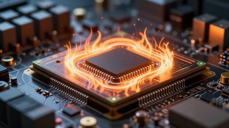
Silicon MOSFETs have served as the backbone of power electronics for decades, but they are increasingly reaching their physical limits. The core issue lies in the intrinsic bandgap energy of silicon, which restricts the operating temperature and power density of traditional UPS modules. As power demands escalate, silicon devices require increasingly bulky heatsinks and active cooling systems to prevent thermal runaway, directly contradicting the industry push for compact, modular infrastructure.
Switching Losses and Frequency Constraints
The primary operational bottleneck in legacy UPS systems is the trade-off between switching frequency and efficiency. Silicon devices exhibit high switching losses, meaning that increasing the frequency to reduce the size of passive components—such as inductors and capacitors—results in excessive heat generation. Consequently, traditional designs are tethered to lower switching frequencies, effectively locking the architecture into a larger physical footprint.
| Constraint | Silicon MOSFET Impact | Resulting Design Outcome |
|---|---|---|
| Bandgap Energy | Low (1.1 eV) | High thermal dissipation needs |
| Switching Frequency | Limited (< 50-100 kHz) | Large, heavy magnetic components |
| On-Resistance | Higher at high temps | Increased conduction losses |
Common Limitations FAQ
- Why can't we just increase the switching frequency on silicon-based boards?
Higher switching frequencies significantly increase switching losses in silicon, leading to unmanageable heat loads that threaten component reliability and board integrity. - Does the size of passive components dictate the size of the entire UPS?
Yes, because silicon requires lower switching frequencies, the inductors and capacitors must be physically larger to handle power loads, preventing the miniaturization of the entire UPS unit. - How does conduction resistance impact power density?
As silicon devices heat up, their on-resistance increases, causing a cycle of efficiency loss that forces engineers to limit total power output per rack unit to prevent failure.
Understanding Wide-Bandgap Semiconductors
The Physics of Bandgap Superiority
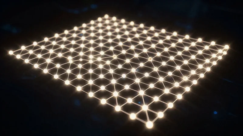
Wide-bandgap (WBG) materials, specifically Gallium Nitride (GaN) and Silicon Carbide (SiC), possess a larger energy gap between the valence band and the conduction band compared to traditional silicon. This fundamental material property allows electrons to gain enough energy to cross the bandgap at significantly higher temperatures and voltages. Consequently, power components constructed with WBG materials can operate at much higher frequencies and thermal thresholds while exhibiting lower on-resistance, effectively redefining the efficiency ceiling for UPS power conversion modules.
Comparative Material Properties
| Property | Silicon (Si) | Gallium Nitride (GaN) | Silicon Carbide (SiC) |
|---|---|---|---|
| Bandgap (eV) | 1.1 | 3.4 | 3.2 |
| Breakdown Field (MV/cm) | 0.3 | 3.3 | 2.5 |
| Thermal Conductivity | Moderate | High | Very High |
| Switching Speed | Slow | Extremely Fast | Fast |
Key Advantages for UPS Architecture
- Increased Power Density
The superior breakdown field strength allows WBG components to be manufactured in smaller dies, drastically reducing the physical footprint of UPS power stages. - Reduced Thermal Management Requirements
Lower conduction losses mean less heat is generated, allowing for smaller heat sinks, smaller cooling fans, and overall simplified thermal management systems. - Higher Switching Frequencies
By operating at higher frequencies, the size of passive components like inductors and capacitors can be reduced, significantly lowering the total weight and volume of the UPS.
Impact on PCB Layout and Component Density
Shrinking the Passive Footprint
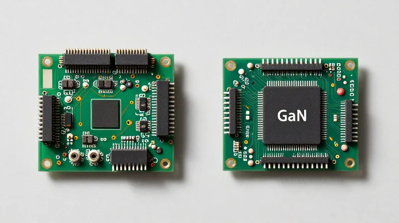
The primary catalyst for density improvements in GaN-based UPS systems is the capacity for high-frequency switching. In traditional silicon designs, switching frequencies are typically capped to minimize switching losses, necessitating large, bulky inductors, transformers, and capacitors to manage energy storage and ripple current. By utilizing GaN's superior electron mobility, engineers can push switching speeds into the megahertz range. This transition inversely correlates with the required volume of passive components, allowing for smaller board real estate and a significantly more compact power stage.
Comparative Impact on PCB Design
| Feature | Silicon-Based Design | GaN-Based Design |
|---|---|---|
| Switching Frequency | Low (20kHz - 100kHz) | High (>500kHz - 2MHz) |
| Passive Size | Large (Bulky Magnetics) | Small (Surface Mount Magnetics) |
| PCB Footprint | Extensive | Highly Compact |
| Thermal Density | Distributed Heat | Concentrated but Efficient |
Layout Considerations and Challenges
While GaN technology enables drastic reductions in board size, it introduces new complexities in PCB layout. Because GaN devices switch at significantly higher speeds, parasitic inductance becomes a critical design bottleneck. Minimizing current loops is paramount to prevent voltage spikes that could lead to EMI issues or gate oscillation. Design teams must transition to advanced multilayer PCB stacks, prioritizing tight coupling between power and ground planes to manage these high-speed transients effectively.
Frequently Asked Questions
- Does higher frequency operation increase EMI issues?
Yes, high-speed switching generates higher-order harmonics, which can exacerbate EMI. However, modern PCB design techniques and integrated power module packaging are effectively mitigating these risks. - Why does reducing passive size improve UPS reliability?
By reducing the number and size of bulky components, the mechanical stress on the PCB is lowered and thermal pathways can be optimized, leading to a more robust system under vibration and temperature cycling. - Can GaN replace silicon in existing UPS form factors?
GaN allows for the same power density in a smaller footprint, but can also be used to significantly increase power density within existing standard rack-mount chassis sizes, maximizing data center uptime.
Thermal Management Challenges in Next-Gen Designs
Thermal Management Challenges in Next-Gen Designs
As UPS power systems transition from traditional silicon-based architectures to high-frequency Gallium Nitride (GaN) platforms, the primary thermal challenge shifts from bulk heat dissipation to localized power density management. While GaN components offer superior efficiency—significantly reducing switching losses—their drastically smaller physical footprints concentrate heat into localized 'hot spots.' Engineers must now transition from traditional convection-based cooling toward high-conductivity thermal interface materials and optimized PCB copper trace geometry to prevent thermal throttling and ensure long-term reliability in compact enclosures.
Thermal dissipation strategies: Silicon vs. GaN
| Feature | Traditional Silicon Design | Next-Gen GaN Design |
|---|---|---|
| Heat Distribution | Distributed across large MOSFET area | Concentrated at micro-scale junctions |
| Primary Cooling Need | Airflow over bulk heatsinks | Substrate-level heat spreading |
| PCB Requirement | Standard FR4 / thick copper | High thermal conductivity metal-core PCBs |
Frequently Asked Questions
- Why does high-frequency GaN switching increase thermal stress?
While GaN reduces overall power loss, the extreme power density in a small package creates high heat flux densities that exceed the spreading capabilities of standard substrate materials. - How does PCB layout impact GaN thermal performance?
Proper layout requires integrating thermal vias directly under the GaN die and utilizing heavy copper pours to act as primary heat sinks, effectively bypassing the limitations of traditional air-cooled architectures. - Is active cooling still required for GaN-based UPS systems?
While GaN operates more efficiently, the reduction in system size usually leads to higher energy density, meaning airflow management remains critical, though it can be optimized for lower noise and smaller fan profiles.
Electromagnetic Interference (EMI) Mitigation Strategies
The Challenge of High-Speed Switching
Gallium Nitride (GaN) transistors switch at significantly higher speeds than traditional silicon MOSFETs. While this enables greater efficiency and power density, it also introduces substantial electromagnetic interference (EMI). The rapid voltage transitions (dv/dt) and current changes (di/dt) create parasitic ringing and high-frequency noise that can disrupt sensitive control circuitry and violate stringent regulatory standards.
Best Practices for Signal Integrity
- Minimizing Power Loop Inductance
Place decoupling capacitors as physically close to the GaN device as possible. Utilizing a vertical loop design on adjacent PCB layers can reduce the total loop area, which is the primary source of radiated EMI. - Optimizing Gate Drive Paths
Keep gate drive loops extremely tight to prevent parasitic inductance from causing unwanted oscillations that lead to false triggering or gate overvoltage. - Strategic Ground Plane Implementation
Utilize a solid, uninterrupted ground plane directly beneath high-speed components to provide a low-impedance return path for high-frequency currents, minimizing common-mode noise.
Mitigation Strategy Comparison
| Strategy | Targeted Interference Type | Implementation Difficulty |
|---|---|---|
| Shielding & Faraday Cages | Radiated EMI | Moderate |
| Common-Mode Chokes | Conducted EMI | Low |
| Gate Resistor Tuning | Switching Ringing/Oscillation | High |
| Low-ESL Capacitors | High-Frequency Noise | Low |
Regulatory Compliance FAQ
- Does GaN make FCC/CISPR compliance harder?
Yes, because the higher frequency spectrum contains more energy. However, through careful PCB layout, GaN designs often achieve better efficiency, reducing the overall thermal footprint which simplifies housing design. - When is active EMI filtering necessary?
When passive components like ferrites and common-mode chokes are insufficient to meet regulatory limits due to space constraints or high-power frequency requirements.
Cost-Benefit Analysis for Infrastructure Planning

The Economic Trade-off: Capital Expenditure vs. Operational Efficiency
While Gallium Nitride (GaN) power transistors currently command a premium over traditional Silicon (Si) MOSFETs, the economic argument for their adoption in modern UPS systems is shifting from unit cost to system-level value. By enabling higher switching frequencies, GaN allows for the radical downsizing of passive components—such as inductors and capacitors—which significantly reduces the bill of materials (BOM) for these supporting elements. Organizations must move beyond comparing individual semiconductor prices and instead adopt a total cost of ownership (TCO) methodology that accounts for footprint reduction, energy savings, and thermal management overhead.
| Financial Metric | Traditional Silicon (Si) PCB | Next-Gen Gallium Nitride (GaN) PCB |
|---|---|---|
| Component Cost | Low/Stable | Premium |
| Passive Component Size | Large/Expensive | Small/Cost-Efficient |
| Energy Efficiency | Standard (92-95%) | High (97% +) |
| Thermal Management | Complex/Heavy | Simplified/Lighter |
| Total Footprint | Standard | Up to 50% Smaller |
Key Considerations for Infrastructure Planning
- Does the smaller PCB footprint lead to real estate savings?
Yes. By increasing power density, GaN-based UPS systems can fit higher power ratings into smaller racks, directly reducing data center floor space requirements and lowering facility leasing costs over time. - How does energy efficiency impact the bottom line?
Even a 2% improvement in UPS efficiency results in massive operational savings at scale by reducing the electricity consumed and the corresponding load on cooling infrastructure. - What are the hidden maintenance benefits?
GaN systems operate with lower thermal stress on internal components, extending the service life of critical infrastructure and reducing the frequency of unscheduled repairs.
Infrastructure planners should prioritize long-term utility over short-term procurement expenses. The integration of GaN technology is not merely a component upgrade; it is a fundamental shift toward more sustainable, efficient, and compact power distribution architectures that future-proof data centers against rising energy costs.
Future-Proofing Your UPS Strategy
The Strategic Shift Toward GaN Integration
Transitioning to Gallium Nitride (GaN) is not merely a component upgrade; it is an architectural evolution. Engineering teams must adopt a 'systems-first' approach, where power density is decoupled from physical bulk, allowing for more modular, hot-swappable, and intelligent UPS designs that can adapt to changing load requirements without complete hardware overhauls.
Comparative Framework: Legacy vs. Next-Gen Architectures
| Feature | Traditional Silicon (PCB) | Next-Gen GaN Architecture |
|---|---|---|
| Switching Frequency | Low (up to 100 kHz) | Ultra-High (MHz range) |
| Cooling Demand | Heavy/Active Cooling | Reduced Thermal Footprint |
| Scalability | Fixed Rigid Design | Modular/Software-Defined |
Operational Best Practices for Engineers
- Embrace Software-Defined Power
Move away from hardwired control logic. Implement digital control loops that can be updated via firmware to optimize for evolving GaN thermal behaviors and efficiency curves. - Prioritize High-Frequency Magnetics
Ensure your magnetics supply chain is aligned with GaN capabilities. Using legacy inductors will negate the efficiency gains provided by high-speed GaN switching. - Modular Redundancy Protocols
Design with N+1 or N+X redundancy in mind. GaN allows for smaller form factors, enabling more power modules to fit within the same rack footprint, enhancing reliability.
Addressing Common Implementation Hurdles
- How do we mitigate the risk of supply chain volatility for GaN?
Establish multi-vendor qualification early in the design cycle. Given the specialized nature of GaN, maintaining dual-source paths for power transistors is critical to long-term sustainability. - Is GaN ready for high-reliability enterprise environments?
Yes, provided testing protocols are updated to include high-speed transient response and EMI verification, which are more sensitive in GaN-based systems than in silicon.
The transition to GaN-based UPS design is no longer a luxury but a strategic necessity for high-density power environments. By embracing higher efficiency and smaller footprints, firms can significantly lower their cooling costs and improve system reliability. Ready to upgrade your power infrastructure? Contact our engineering team today for a consultation on your next PCB design project.
