
As industrial automation demands higher efficiency and smaller footprints, the limitations of traditional Silicon-based VFD technology are becoming glaringly apparent. Enter Silicon Carbide (SiC)—a wide bandgap material that is not just an incremental improvement, but a paradigm shift in power electronics. This article explores how SiC is forcing a complete redesign of PCB architectures to unlock unparalleled power density and control.
The Limitations of Traditional Silicon-Based VFDs
The Thermal Ceiling of Silicon
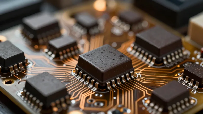
The primary limitation of traditional silicon IGBTs and MOSFETs lies in their physical material properties, specifically their relatively low bandgap energy and thermal conductivity. As power density requirements increase in modern VFD PCB designs, silicon-based power modules face significant cooling challenges. These devices typically operate at junction temperatures below 150°C, necessitating oversized heatsinks and active cooling systems that counteract the industry goal of component miniaturization.
Switching Frequency and Efficiency Trade-offs
Silicon transistors exhibit high switching losses, particularly at high frequencies. Because silicon devices have higher parasitic capacitance and longer reverse recovery times, engineers are often forced to choose between efficiency and performance. Operating at higher frequencies enables smaller passive components but leads to excessive heat generation, while lower frequencies increase motor noise and reduce control precision.
| Feature | Silicon (Si) Limitations | Impact on VFD Design |
|---|---|---|
| Bandgap Energy | Low (1.1 eV) | Higher leakage at high temps |
| Switching Speed | Slow (Reverse recovery) | Increased switching losses |
| Thermal Conductivity | Moderate | Requires bulky thermal management |
Common Industry Questions
- Why can't we just increase switching frequencies with standard silicon?
Increasing switching frequencies in silicon increases switching losses exponentially. This results in excessive heat that standard PCB thermal vias and heat sinks cannot dissipate effectively without significantly increasing device size. - Does silicon reach its limit in all motor control applications?
No, silicon remains cost-effective for low-power and low-speed applications. However, in modern high-performance motor control where space and efficiency are at a premium, silicon is failing to meet the evolving energy density requirements of next-gen industrial systems.
Why Silicon Carbide (SiC) is a Game Changer

The Material Advantage: Why SiC Surpasses Traditional Silicon
The fundamental superiority of Silicon Carbide (SiC) lies in its nature as a wide-bandgap (WBG) semiconductor. While standard silicon requires significant energy to excite electrons into the conduction band, SiC possesses a much wider gap, allowing it to operate under extreme voltages, temperatures, and frequencies that would cause traditional IGBTs to fail. This physical robustness directly translates into smaller, more efficient VFD PCB architectures.
Performance Comparison: Si vs. SiC
| Feature | Silicon (Si) | Silicon Carbide (SiC) |
|---|---|---|
| Bandgap Energy | 1.1 eV | 3.2 eV |
| Breakdown Field | Moderate | Extremely High |
| Thermal Conductivity | Standard | 3x Higher |
| Switching Speeds | Limited | Ultra-Fast |
Key Operational Benefits
- Reduced Conduction and Switching Losses
SiC devices exhibit significantly lower resistance when 'on,' reducing heat generation during high-load operations and allowing for smaller, lighter cooling systems on the PCB. - Higher Switching Frequencies
The ability to switch at much higher speeds allows for the miniaturization of passive components like inductors and capacitors, leading to a drastically reduced PCB footprint. - Enhanced Thermal Management
With higher thermal conductivity, SiC can operate reliably at junction temperatures exceeding 175°C, simplifying the thermal design of motor control units.
Impact on Next-Generation Motor Control
By adopting SiC, engineers are no longer constrained by the thermal ceilings of silicon. This enables the design of high-density VFDs that integrate more power into a smaller volume, essential for modern automation, electric vehicles, and robotics where space is at a premium and energy efficiency is a primary competitive metric.
Thermal Management Challenges in Compact PCB Layouts
The Thermal Density Dilemma
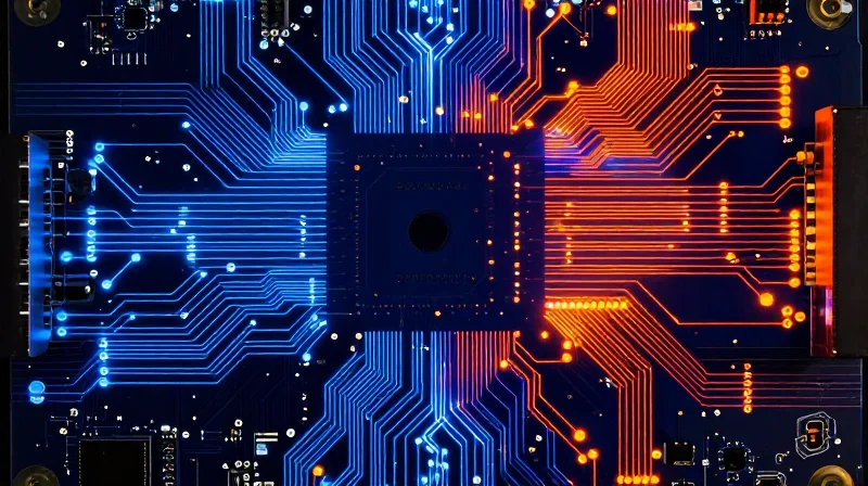
As Variable Frequency Drive (VFD) technology transitions to Silicon Carbide (SiC) MOSFETs, power density has surged, allowing for significant reduction in module footprints. However, this miniaturization creates intense localized heat concentrations that traditional FR-4 substrate materials and standard copper trace configurations cannot adequately manage. The primary engineering challenge lies in transporting thermal energy away from the semiconductor junction before it exceeds the thermal ceiling, which is critical for preventing premature component failure and degradation of dielectric strength.
Advanced Thermal Mitigation Strategies
To address these high heat flux levels, modern PCB layouts incorporate a multi-layered approach to thermal management. The industry is moving away from standard laminates toward Metal Core PCBs (MCPCBs) and ceramic substrates like Alumina (Al2O3) or Aluminum Nitride (AlN), which provide superior thermal conductivity.
| Material Property | Standard FR-4 | Aluminum Nitride (AlN) | Insulated Metal Substrate |
|---|---|---|---|
| Thermal Conductivity (W/mK) | 0.25 - 0.35 | 150 - 200 | 1.0 - 5.0 |
| Dielectric Strength | High | Moderate | Moderate |
| Cost Profile | Low | High | Medium |
Furthermore, the implementation of dense thermal via arrays directly beneath the SiC dies has become standard practice. These vias, often filled with conductive epoxies or copper plating, act as thermal conduits to the bottom-side heat sink, effectively reducing the thermal resistance path from the junction to the ambient environment.
- Why is standard FR-4 insufficient for SiC-based VFDs?
Standard FR-4 has extremely low thermal conductivity, which leads to rapid heat accumulation beneath high-power SiC MOSFETs, potentially causing delamination or thermal runaway. - What role do thermal vias play in compact layouts?
Thermal vias provide a low-resistance path through the PCB stack-up, allowing heat to bypass the insulating layers and transfer directly to a copper plane or heat sink. - How does PCB thickness affect thermal performance?
Reducing dielectric thickness between the component and the metal backing layer significantly lowers thermal impedance, though it requires careful management of voltage isolation clearances.
High-Speed Switching and Parasitic Inductance
The Dual Challenge of Speed and Parasitics
As Variable Frequency Drives transition to Silicon Carbide (SiC) power modules, the primary design hurdle shifts from mere thermal dissipation to the management of high-frequency transients. The extremely fast switching times—often measured in nanoseconds—generate high $dv/dt$ rates that interact with parasitic inductances within the PCB layout, leading to significant voltage overshoot, ringing, and electromagnetic interference (EMI).
Engineering for Signal Integrity
Minimizing loop area is the golden rule for high-frequency design. Even small parasitic inductances in the power loop can cause substantial energy spikes when switched at SiC speeds. Engineers must employ low-inductance busbar architectures and symmetrical power planes to cancel magnetic fields and ensure clean gate drive signals.
| Parameter | Legacy IGBT Design | SiC MOSFET Design |
|---|---|---|
| Switching Speed ($dv/dt$) | Low (5-10 V/ns) | High (>50 V/ns) |
| Voltage Overshoot Sensitivity | Moderate | Critical |
| EMI Mitigation Complexity | Manageable | High (Requires Advanced Layout) |
| Inductance Tolerance | High | Ultra-low |
Frequently Asked Questions
- How does parasitic inductance affect SiC performance?
Parasitic inductance reacts with the rapid current changes of SiC devices to create L*di/dt voltage spikes, which can exceed the breakdown voltage of the MOSFET and increase electromagnetic noise. - What layout strategies best mitigate EMI in VFDs?
Utilizing multi-layer boards with closely coupled return paths, implementing Kelvin source connections for gate drivers, and placing decoupling capacitors as close to the power switch as possible are essential. - Why is gate drive stability more difficult with SiC?
Because SiC switches faster, any inductance in the gate loop can trigger parasitic turn-on due to Miller effect oscillations, necessitating precise, low-impedance drive circuitry.
The Evolution of Gate Driver Circuitry

The Shift Toward High-Performance Gate Drivers
The adoption of Silicon Carbide (SiC) MOSFETs in VFDs introduces switching speeds that far exceed traditional Silicon IGBTs. While these speeds enhance system efficiency and allow for smaller passive components, they place immense strain on gate driver architecture. Modern drivers must now operate in an environment characterized by extremely steep dV/dt transitions, which can cause significant electromagnetic interference (EMI) and unintended cross-conduction if not managed with sub-nanosecond precision.
Critical Engineering Requirements for SiC Drivers
To ensure reliable operation with SiC-based power stages, gate drivers have evolved to include specialized features that maintain signal integrity while protecting the sensitive gate oxides of SiC devices.
| Requirement | Challenge | Driver Solution |
|---|---|---|
| Common Mode Transient Immunity (CMTI) | High dV/dt induces false switching | Enhanced isolation (>100kV/µs) |
| Miller Clamp | Voltage spikes at the gate | Active Miller clamping circuits |
| Short Circuit Protection | Fast SiC fault propagation | Desaturation monitoring (<1µs reaction) |
Mitigating Parasitic Effects in Layout
The evolution of VFD gate drivers is not limited to the component level; it extends to the PCB layout interface. Minimizing the loop area between the gate driver and the power semiconductor is essential to suppress ringing caused by source inductance. Integrated gate driver modules that mount directly onto the PCB, as close as possible to the power devices, are becoming the industry standard to maintain the gate loop impedance required for stable SiC operation.
Frequently Asked Questions
- Why is dV/dt robustness so critical for SiC?
SiC devices switch so rapidly that they create voltage transients capable of inducing noise into the gate circuit, which can lead to catastrophic shoot-through events. - Do I need negative gate bias for SiC drivers?
Yes, implementing a negative gate drive voltage is a standard practice to suppress the effects of the Miller capacitance and prevent parasitic turn-on of the SiC MOSFET. - How does isolation impact VFD reliability?
High-speed galvanic isolation is vital to separate high-voltage power paths from low-voltage logic, ensuring that high-frequency noise does not compromise the control CPU.
Optimizing PCB Layout for Power Density

Strategies for High-Density Power Integration
To maximize power density in SiC-driven VFDs, designers must transition from traditional layout paradigms to advanced 3D-integrated approaches. The primary objective is to minimize the commutation loop inductance, which is directly responsible for voltage spikes that degrade efficiency and threaten component reliability during high-frequency switching. By leveraging vertical power looping and multi-layer copper pour strategies, engineers can significantly reduce the footprint of high-power modules while maintaining necessary creepage and clearance distances.
Copper Weight and Thermal Distribution
| Parameter | Standard VFD PCB | Next-Gen SiC VFD PCB |
|---|---|---|
| Copper Thickness | 1-2 oz | 3-6 oz (or Embedded Busbars) |
| Via Strategy | Single-sided thermal | Copper-filled micro-via arrays |
| Component Pitch | Low density | High density with localized decoupling |
Advanced layouts utilize thicker copper weight (3 oz to 6 oz) or internal embedded busbars to handle high current densities without excessive resistive heating. Integrating thermal via arrays directly beneath the SiC MOSFETs serves to pull heat into the inner layers, effectively turning the entire PCB substrate into a functional heat spreader.
Frequently Asked Questions on Layout Optimization
- How does PCB layout impact SiC dV/dt performance?
Poor layout causes parasitic oscillations during switching transitions; maintaining tight, symmetrical loop paths is essential to suppress ringing caused by high dV/dt transients. - Is internal copper thickness sufficient for thermal management?
While thicker copper reduces resistance, it must be paired with high-thermal-conductivity substrates (such as IMS or ceramic-filled laminates) to effectively transport heat to the chassis. - What is the role of vertical placement?
Vertical power loops reduce the physical area of the current path, minimizing loop inductance and facilitating a smaller total component footprint by stacking decoupling capacitors near the power stage.
Reliability and Longevity in Harsh Industrial Environments
Thermal Resilience and Material Superiority
The transition to Silicon Carbide (SiC) in VFD PCBs fundamentally alters the thermal envelope of industrial drives. Unlike traditional silicon-based IGBTs, SiC MOSFETs exhibit a significantly higher bandgap, allowing components to operate at elevated temperatures with minimal leakage current. This intrinsic material property reduces the reliance on aggressive active cooling systems, lowering the mechanical complexity of the drive and minimizing failure points associated with fan bearings and heat exchanger blockages in dusty or humid environments.
Comparative Reliability Profile
| Parameter | Traditional Silicon (IGBT) | Next-Gen Silicon Carbide (SiC) |
|---|---|---|
| Max Junction Temp | 150°C | 200°C+ |
| Switching Losses | High | Ultra-Low |
| Thermal Conductivity | Standard | 3x Higher |
| PCB Stress | High due to heat | Low due to efficiency |
Mitigating Longevity Challenges in Industrial Settings
While SiC offers superior thermal performance, it imposes stricter requirements on the PCB dielectric materials and insulation coordination due to higher dV/dt transitions. To ensure long-term longevity, next-generation VFD designs are shifting toward high-CTI (Comparative Tracking Index) PCB laminates that resist carbon tracking and dendrite growth when exposed to conductive dust or condensation. By combining SiC switches with advanced encapsulation techniques, manufacturers can prevent localized hotspots that typically degrade traditional epoxy-based components over a 10-20 year service life.
Frequently Asked Questions
- How does SiC affect capacitor aging?
Lower switching losses and reduced operating temperatures in SiC-based drives significantly extend the service life of DC-link capacitors, which are often the primary cause of VFD failure. - Are special coatings required for SiC PCBs?
Yes, high dV/dt levels necessitate advanced conformal coatings with high dielectric strength to prevent partial discharge and corona effects, especially in high-altitude or high-humidity applications.
The Future Outlook: Toward Smarter, Integrated Drive Systems

Convergence of Edge Computing and Drive Electronics
The next frontier in motor control lies in migrating computational intelligence from centralized PLCs directly onto the VFD PCB. By embedding low-latency microcontrollers and AI-capable chipsets onto the drive board, systems can process high-frequency motor feedback locally. This edge-level intelligence allows for real-time adjustments to PWM switching patterns, compensating for thermal fluctuations or load transients with microsecond precision, ultimately minimizing harmonic distortion and energy loss.
Smart Sensor Integration and Digital Twin Synchronicity
Advanced PCB design is now incorporating monolithic sensor arrays—including MEMS-based vibration, acoustic, and thermal sensors—directly into the power stage. These sensors capture granular data that, when processed through an edge-enabled firmware model, enables the creation of an accurate digital twin of the motor system in real-time. This integration shifts the paradigm from reactive maintenance to prescriptive self-optimization.
| Feature | Legacy Drive System | Smart Integrated System |
|---|---|---|
| Data Processing | Centralized (PLC) | Edge (PCB-level) |
| Sensor Feedback | External/Analog | Integrated/Digital |
| Optimization | Static Profiles | Real-time Self-tuning |
| Maintenance | Scheduled | Predictive/Prescriptive |
Frequently Asked Questions
- How does edge computing improve VFD energy efficiency?
By processing control loops locally on the PCB, latency is reduced to near-zero, allowing the drive to optimize switching frequencies dynamically based on instantaneous demand rather than averaged historical profiles. - Does integrating smart sensors on a power PCB create interference risks?
It does pose challenges, but modern PCB architectures utilize high-speed differential signaling and advanced galvanic isolation to ensure that sensitive logic traces remain immune to the switching noise generated by SiC power stages. - What is the ultimate benefit of a self-optimizing drive?
Self-optimization leads to extended equipment lifespan, reduced downtime through early failure detection, and the ability to operate motors at their peak efficiency point regardless of varying environmental or load conditions.
The migration to Silicon Carbide is essential for any company aiming to remain competitive in the rapidly evolving industrial automation market. By embracing next-gen PCB architectures, engineers can achieve superior power density and efficiency. Contact our engineering team today to learn how we can integrate these advanced semiconductor solutions into your next motor control project.
