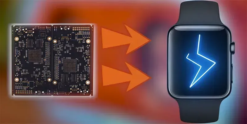
In today's fast-paced world, smartwatches have become indispensable companions, seamlessly integrating into our daily lives. At the heart of every smartwatch lies its motherboard, a marvel of engineering that packs immense functionality into a tiny space. As Zero One Solution Limited, we recognize the critical role these miniature PCBs play and are dedicated to providing cutting-edge Smartwatch Motherboard Solutions. We're not just talking about PCBs; we're talking about enabling the future of wearable technology. This article dives into the intricacies of smartwatch motherboard technology, exploring design challenges, manufacturing processes, and the innovative solutions Zero One Solution offers to empower your wearable creations.
The Growing Demand for Advanced Smartwatch Technology
The burgeoning market for smartwatches is driving an unprecedented demand for increasingly sophisticated and miniaturized motherboard solutions. These compact powerhouses are critical enablers for the ever-expanding suite of advanced functionalities, from health monitoring and contactless payments to enhanced connectivity and seamless user experiences. As consumers expect more from their wrist-worn devices, the underlying PCB technology must evolve rapidly to support greater processing power, more sensors, and extended battery life within incredibly confined spaces.
Explosive Market Growth The global smartwatch market is projected to reach over 150 million units shipped by 2027, with a Compound Annual Growth Rate (CAGR) exceeding 15% (Source: Statista, IDC reports). This surge is fueled by increased health consciousness, the convenience of wearable tech, and advancements in feature sets.
Miniaturization Imperative The core challenge in meeting this demand lies in miniaturization without compromising performance. Smartwatch motherboards must integrate a multitude of components—processors, memory, sensors, wireless modules—into a footprint often smaller than a postage stamp, necessitating advanced PCB manufacturing techniques like HDI (High-Density Interconnect) and specialized material selection.
Feature Integration vs. Size Constraints Modern smartwatches now incorporate ECG, SpO2, body temperature sensors, GPS, NFC, and cellular connectivity. Each added feature demands dedicated circuitry and processing power, intensifying the need for ultra-compact and highly efficient motherboard designs that can manage complex signal routing and thermal dissipation within tight spatial limitations.
Energy Efficiency and Battery Life User expectation for multi-day battery life directly impacts motherboard design. Low-power components and intelligent power management circuitry must be integrated without increasing board size or complexity, presenting a significant design challenge that influences component placement and trace routing.
Smartwatch Feature
Motherboard Impact
Benefit to User
Advanced Health Monitoring (ECG, SpO2)
Requires precise analog front-end circuits, multiple sensor interfaces, and powerful data processing units in a small footprint.
Comprehensive insights into health and well-being, early detection of potential issues.
Cellular Connectivity (LTE/5G)
Demands complex RF modules, antennae integration, and robust power delivery networks for continuous connectivity, all within tight board space.
Untethered communication, streaming, and emergency services directly from the wrist.
Contactless Payments (NFC)
Integrates secure element chips, NFC antennas, and shielded routing to prevent interference, necessitating careful layout for reliable transactions.
Convenient and secure transactions without needing a phone or wallet.
Enhanced GPS/GNSS
Requires compact, high-performance GNSS modules and optimized antenna placement for accurate location tracking, often with low-power requirements.
Precise outdoor activity tracking, navigation, and location-based services.
Key Challenges in Smartwatch Motherboard Design
Designing smartwatch motherboards presents a unique set of engineering challenges due to the stringent requirements for miniaturization, performance, and reliability in a confined space. Unlike traditional PCB designs, smartwatch motherboards demand an exceptionally high component density, efficient thermal dissipation within a tiny enclosure, and impeccable signal integrity to support advanced functionalities like health monitoring, GPS, and wireless communication, all while maintaining a sleek form factor and extended battery life. Addressing these inherent complexities requires a deep understanding of advanced PCB technologies and meticulous design considerations to ensure the device's optimal performance and longevity.
Challenge Area
Description
Impact on Smartwatch Design
Miniaturization & Component Density
Packing numerous complex functionalities into an extremely small form factor, requiring ultra-fine pitch components and multi-layer PCBs.
Limits space for components, requires advanced routing, and necessitates innovative packaging solutions for ICs and sensors to maintain a compact design.
Challenge Area
Description
Impact on Smartwatch Design
Thermal Management
Dissipating heat generated by high-performance processors, displays, and communication modules within a sealed, compact enclosure to prevent overheating and ensure stable operation.
Can lead to performance throttling, reduced component lifespan, and user discomfort if not effectively managed through optimized material selection, thermal vias, and heat spreading techniques.
Challenge Area
Description
Impact on Smartwatch Design
Signal Integrity
Maintaining the quality of high-speed signals across dense layouts and complex interconnections to prevent data loss, crosstalk, and electromagnetic interference (EMI) in RF, digital, and analog circuits.
Crucial for reliable wireless communication (Bluetooth, Wi-Fi, NFC), accurate sensor readings, and stable data processing, requiring careful impedance control, trace routing, and grounding strategies.
At the heart of every groundbreaking smartwatch lies a marvel of miniaturized engineering: the motherboard. Achieving the compact size, power efficiency, and robust functionality demanded by modern wearable technology requires unparalleled expertise in advanced PCB solutions. Zero One Solution Limited stands as a beacon in this specialized field, leveraging over a decade of experience since our founding in 2011 to deliver rapid prototyping, manufacturing, and assembly services specifically tailored for the intricate requirements of wearable devices.
Our strategic presence in Shenzhen, China, and Dubai positions us uniquely within the global PCBA supply chain, granting seamless access to cutting-edge technologies and resources. This global network, combined with our relentless focus on R&D prototype manufacturing, empowers our clients to accelerate their product development cycles and introduce innovative smartwatch solutions to market with remarkable efficiency. We understand that in the fast-paced world of wearables, time-to-market is critical, and our end-to-end capabilities ensure a streamlined journey from concept to reality.
Rapid Prototyping Excellence Zero One Solution excels in rapid-response R&D prototyping, enabling quick iteration and validation of smartwatch motherboard designs. Our agility helps clients significantly reduce development timelines, turning innovative concepts into tangible prototypes faster than competitors.
Specialized for Wearables Unlike general PCB manufacturers, we possess deep expertise in the unique challenges of wearable technology, including extreme miniaturization, high component density, and stringent power management requirements. Our solutions are engineered from the ground up for smartwatch applications.
One-Stop Integrated Services From initial PCB design and layout optimization to advanced manufacturing and precise assembly, Zero One Solution provides a comprehensive, integrated service. This holistic approach minimizes coordination complexities and ensures seamless project execution for smartwatch developers.
Global Supply Chain Advantage Our dual presence in Shenzhen, the global electronics manufacturing hub, and Dubai, a strategic logistics gateway, grants unparalleled access to a diverse range of high-quality materials and components, ensuring supply chain resilience and cost-effectiveness for smartwatch production.
High-Density Interconnect (HDI) Technology for Smartwatches
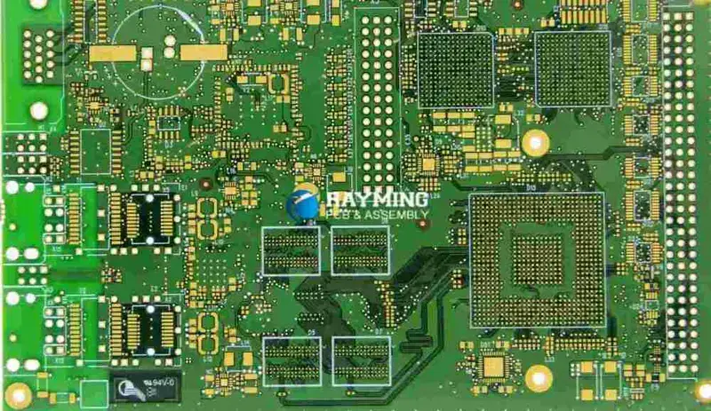
Smartwatch HDI PCB
High-Density Interconnect (HDI) technology is pivotal in revolutionizing smartwatch motherboard design, allowing for the unprecedented integration of advanced functionalities within the inherently limited space of wearable devices. This sophisticated PCB manufacturing technique enables a significant increase in component density and routing capabilities, which is absolutely critical for the compact yet feature-rich smartwatches demanded by today's market. By reducing board size while enhancing performance, HDI PCBs are the backbone of modern smartwatch innovation, addressing the core challenge of miniaturization without compromising on power or functionality. This approach ensures that complex features, from advanced sensors to wireless communication modules, can be seamlessly integrated, leading to more powerful and versatile devices.
Enhanced Miniaturization HDI technology achieves significant size reduction through finer lines and spaces, smaller vias, and higher routing density, enabling more compact and aesthetically pleasing smartwatch designs without sacrificing performance. This allows for a greater component count within a smaller footprint, essential for advanced wearable features.
Improved Signal Integrity Shorter electrical paths and controlled impedance offered by HDI designs minimize signal degradation, crosstalk, and electromagnetic interference (EMI), which are crucial for the high-frequency operations of smartwatch components like wireless communication modules and high-resolution displays. This ensures reliable data transmission and optimal device performance.
Increased Functionality and Performance By allowing for greater component density and more complex circuitry, HDI PCBs facilitate the integration of advanced features such as multiple health sensors, GPS modules, NFC for payments, and longer-lasting batteries into smartwatches, enhancing overall functionality and user experience. This level of integration would be unachievable with conventional PCB technologies.
Material Selection for Optimal Performance and Reliability
High-Tg FR-4 PCB
The foundation of a high-performance, durable smartwatch motherboard lies in the meticulous selection of its PCB materials. Given the compact nature and demanding operational environment of wearable devices, the chosen materials must provide exceptional thermal stability, ensure robust signal integrity, and exhibit superior mechanical durability to withstand daily use. Zero One Solution Limited prioritizes advanced material science to deliver smartwatch motherboards that meet and exceed these stringent requirements, ensuring prolonged device lifespan and consistent functionality.
Material Type
Key Advantages
Typical Applications in Smartwatches
Considerations
High-Tg FR-4
Excellent thermal resistance, cost-effective, good electrical properties
Standard layers, non-critical signal paths, general power layers
Higher Dk/Df compared to advanced materials, can be limiting for very high frequencies
Polyimide (PI)
Superior thermal stability, low coefficient of thermal expansion (CTE), excellent flexibility (for flex PCBs)
Flexible PCBs for dynamic connections, high-temperature zones, compact modules
Higher cost than FR-4, requires specialized processing for flex circuits
Low-Loss/High-Frequency Laminates
Extremely low dielectric loss (Df), stable dielectric constant (Dk) over frequency, high signal integrity
RF modules (Wi-Fi, Bluetooth, GPS), high-speed data lines
Significantly higher cost, requires precise impedance control during fabrication
Cost-effective compared to high-frequency laminates, good balance of properties
Beyond the core substrate, other material considerations are critical for the overall smartwatch motherboard solution. This includes specialized soldermasks for fine-pitch components, surface finishes like ENIG (Electroless Nickel Immersion Gold) or OSP (Organic Solderability Preservative) for optimal solderability and reliability, and advanced prepreg materials for precise layer stacking and controlled impedance in multi-layer designs. Our comprehensive approach to material selection ensures that every aspect of the smartwatch motherboard is optimized for peak performance and long-term reliability in the demanding wearable market.
Advanced Manufacturing and Assembly Processes
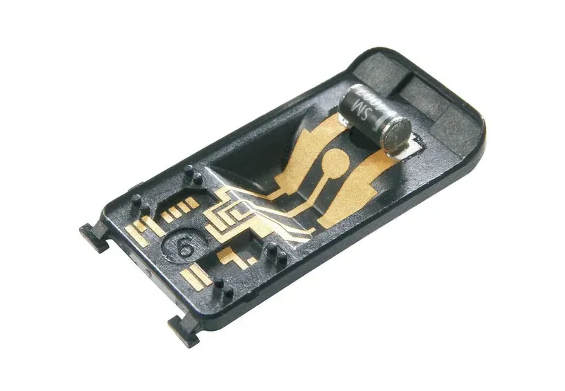
Laser Direct Structuring
Producing high-performance, ultra-compact smartwatch motherboards demands manufacturing and assembly processes that transcend traditional PCB fabrication. Zero One Solution Limited leverages cutting-edge techniques to ensure the reliability, functionality, and miniaturization critical for wearable technology. These advanced methodologies are fundamental to achieving the intricate designs and high component densities required, setting a new standard for precision engineering in the smartwatch industry.
Process
Description
Key Benefit for Smartwatch Motherboards
Laser Direct Structuring (LDS)
A 3D MID (Molded Interconnect Device) technology where laser light structures conductive paths directly onto plastic components. This eliminates the need for a traditional PCB, integrating circuits directly onto the device housing.
Enables highly miniaturized, complex 3D circuits, freeing up internal space and reducing overall device size. Ideal for antenna integration and sensor placement.
Microvia Drilling
The creation of extremely small holes (typically < 150 µm in diameter) through laser drilling, used to connect layers in HDI PCBs. These vias are much smaller than conventionally drilled holes.
Facilitates higher routing density and allows for more compact component placement, crucial for multi-layer smartwatch PCBs with limited footprint.
Precision Component Placement (SMT)
Utilizing high-accuracy pick-and-place machines to position tiny surface-mount components (down to 01005 package sizes) with micron-level precision onto the PCB.
Ensures accurate placement of miniature components like ICs, sensors, and passive elements, vital for proper circuit functionality and overall device reliability.
Beyond these core processes, our capabilities extend to fine-pitch soldering, advanced cleaning protocols, and rigorous in-process quality control. Each step is meticulously calibrated to meet the stringent requirements of smartwatch applications, from ensuring robust solder joints on minute components to maintaining pristine board surfaces for optimal electrical performance. Our integrated approach guarantees that every smartwatch motherboard solution we deliver is not just assembled, but engineered for peak performance and enduring reliability in the demanding wearable environment.
Thermal Management Strategies for Wearable Devices
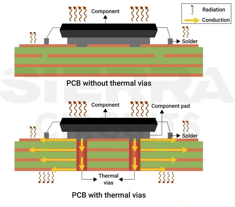
Thermal Via Dissipation
Effective thermal management is paramount for the stable and reliable operation of wearable devices like smartwatches, where miniaturization and high component density lead to significant heat generation. Without proper strategies, excessive heat can degrade performance, shorten battery life, and even damage sensitive components. Implementing robust thermal management solutions is crucial to maintain optimal operating temperatures, ensuring the longevity and consistent functionality of the smartwatch motherboard. This is particularly critical given the close proximity of these devices to the user's skin, making thermal comfort an additional design consideration.
Strategy
Description
Advantages
Disadvantages
Heat Spreaders
Thin, highly conductive plates (e.g., copper, graphite) placed over heat sources to distribute heat evenly across a larger surface area.
Effective for localized hot spots, passive, no power consumption.
Adds thickness and weight, may require additional space, limited heat dissipation without external airflow/sink.
Widely used in compact electronics.
Often combined with other methods.
Common in CPUs and GPUs.
Improves overall thermal uniformity.
Thermal Vias These are small, copper-filled holes in the PCB that create direct thermal paths from heat-generating components to cooler areas or heat sinks, efficiently transferring heat through the board layers. They are particularly effective in multi-layer PCBs for vertical heat dissipation, preventing localized hot spots and improving overall thermal conductivity of the board. Proper sizing and density of thermal vias are crucial for optimal performance, often requiring specialized PCB design software to simulate heat flow and optimize placement for maximum efficiency. Zero One Solution Limited leverages advanced design tools and manufacturing precision to integrate effective thermal via arrays, ensuring optimal heat transfer within the compact smartwatch motherboard architecture, contributing significantly to device longevity and stability under continuous operation, even during intensive tasks such as GPS tracking or continuous heart rate monitoring. Our expertise extends to optimizing via-in-pad technologies, allowing for direct thermal transfer from component pads, which is vital for space-constrained designs where traditional via placement might be challenging. This precise engineering approach is a cornerstone of our rapid prototyping and manufacturing services, enabling our clients to achieve superior thermal performance in their cutting-edge wearable devices without compromising on miniaturization or functionality. Thermal vias are essential for managing heat generated by high-density integrated circuits and power management units within the limited confines of a smartwatch, preventing performance throttling and ensuring user comfort. By facilitating efficient heat egress from critical components, they contribute directly to the device's reliability and extended operational lifespan, mitigating the risks associated with prolonged heat exposure such as component degradation or premature battery aging. The implementation of thermal vias also supports higher power densities, enabling more feature-rich smartwatches without increasing their physical footprint, aligning perfectly with the demands of the rapidly evolving wearable technology market. These highly conductive pathways are crucial in mitigating localized temperature rises, ensuring that even under heavy computational loads or during prolonged usage, the smartwatch maintains its intended performance specifications. The strategic placement and sizing of thermal vias are critical design considerations that directly impact the overall thermal resistance of the PCB, allowing for a more efficient transfer of heat away from critical components and towards the external casing or other heat dissipation elements. This meticulous approach to thermal management is a testament to Zero One Solution's commitment to delivering high-performance, reliable, and compact PCB solutions for the most demanding applications in the wearable technology sector, ensuring that our clients' innovations are not just functional but also durable and user-friendly over their entire lifecycle. The precise engineering of thermal vias allows for targeted heat extraction, preventing hot spots that could otherwise lead to performance throttling or even irreversible damage to sensitive electronic components. Our methodology involves extensive thermal simulations during the design phase to determine the optimal configuration of thermal vias, considering factors such as component power dissipation, PCB material properties, and environmental operating conditions. This proactive approach ensures that the smartwatch motherboard can effectively manage its thermal load, even when pushed to its limits during demanding applications, thus guaranteeing a consistent and reliable user experience. Furthermore, the integration of thermal vias also contributes to improving the overall current carrying capacity of power traces, as lower operating temperatures reduce the electrical resistance of copper, which is an often overlooked benefit of effective thermal management. The ability to precisely control heat flow within such a compact form factor is a key differentiator for Zero One Solution, as it directly impacts the performance, longevity, and user comfort of advanced wearable devices. By minimizing the thermal resistance between the heat source and the heat sink, thermal vias play a pivotal role in maintaining the integrity of the integrated circuits and the stability of the entire system. This meticulous attention to detail in thermal design is what allows our clients to innovate with confidence, knowing that the underlying PCB solution is engineered for peak performance and reliability, even in the most thermally challenging environments presented by modern smartwatches. The strategic deployment of thermal vias not only enhances heat dissipation but also contributes to the overall structural integrity of the PCB, particularly in applications where repeated thermal cycling might otherwise induce mechanical stresses. Our design philosophy prioritizes a holistic approach to thermal management, integrating thermal vias as a fundamental element of a comprehensive heat dissipation strategy, ensuring that the smartwatch motherboard operates within safe temperature limits under all conditions. This advanced thermal design capability underscores Zero One Solution's commitment to delivering cutting-edge PCB solutions that meet the rigorous demands of the wearable technology industry, providing a reliable foundation for next-generation smartwatches and other compact electronic devices.
Ensuring Signal Integrity in High-Frequency Designs
In the realm of compact, feature-rich smartwatches, ensuring signal integrity (SI) in high-frequency motherboard designs is paramount. The densely packed components and rapid data transfer rates inherent to these devices make them highly susceptible to signal degradation, crosstalk, electromagnetic interference (EMI), and impedance mismatches. Maintaining robust signal integrity is not merely an engineering nicety; it is fundamental to the reliable operation, accurate data processing, and extended battery life of the smartwatch, directly impacting user experience and product performance. Without meticulous attention to SI, the advanced functionalities promised by these devices could be severely compromised, leading to system instability or outright failure. Zero One Solution Limited prioritizes advanced design and manufacturing techniques to mitigate these challenges, delivering stable and high-performance smartwatch motherboards.
SI Challenge
Impact on Smartwatch
Mitigation Strategy
Signal Loss (Attenuation)
Reduced data rates, diminished signal strength, potential for data corruption.
Voltage drops and noise on power delivery networks, impacting signal quality and component reliability.
Decoupling capacitors, wide power and ground planes, optimized via distribution for power.
Why is signal integrity particularly challenging in smartwatch motherboards? Smartwatch motherboards present unique signal integrity challenges due to their extreme miniaturization, high component density, multi-layer PCBs, and the integration of diverse high-frequency wireless modules (Bluetooth, Wi-Fi, NFC). These factors contribute to increased proximity of signal traces, complex power delivery networks, and a higher propensity for crosstalk and EMI within a confined space. Balancing performance with compact size necessitates innovative SI engineering practices.
How does Zero One Solution ensure signal integrity during PCB design? Zero One Solution employs a multi-faceted approach. We utilize advanced EDA tools for comprehensive SI simulations during the design phase, allowing for predictive analysis of signal behavior. Our engineers meticulously implement controlled impedance routing, differential signaling, precise layer stack-up definitions, and strategic placement of ground and power planes. We also focus on minimizing via stubs and optimizing trace geometries to reduce reflections and maintain signal fidelity.
What role do materials play in maintaining signal integrity? Material selection is critical. For high-frequency designs, we often recommend low-loss dielectric materials with stable dielectric constants (Dk) and dissipation factors (Df). Materials like certain types of high-Tg FR-4, polyimide, or specialized high-frequency laminates minimize signal attenuation and maintain consistent impedance across varying frequencies, which is vital for reliable data transmission in compact smartwatch environments.
How are thermal effects considered in signal integrity for smartwatches? Thermal management is inherently linked to signal integrity. Temperature variations can alter material properties (like Dk), affecting signal propagation and impedance. Our designs incorporate thermal management strategies, such as optimized copper distribution, thermal vias, and strategic component placement, not only to dissipate heat but also to ensure a stable thermal environment, thereby preserving the integrity of high-frequency signals and preventing performance degradation.
What manufacturing techniques support high signal integrity in smartwatch PCBs? Our advanced manufacturing processes are tailored to support high SI. This includes precision laser drilling for microvias, which reduces stub length and signal reflections; sophisticated lamination processes for consistent dielectric thickness; and stringent quality control during etching to ensure precise trace geometries and impedance control. These precise manufacturing capabilities are essential for translating the SI-optimized design into a high-performance physical board.
Zero One Solution's Comprehensive PCB Solutions for Smartwatches
Zero One Solution Limited stands as a premier partner for smartwatch manufacturers seeking robust and innovative PCB solutions. Our comprehensive, one-stop services encompass the entire product development lifecycle, from initial design and intricate layout to precision manufacturing and sophisticated assembly, ensuring a seamless and efficient journey for even the most complex smartwatch projects. This holistic approach minimizes supply chain complexities and accelerates time-to-market, which is critical in the fast-paced wearable technology industry.
Integrated Design and Layout Services Our expert engineers provide end-to-end design and layout services specifically optimized for the constraints of smartwatch motherboards. This includes meticulous consideration of miniaturization, HDI implementation, thermal management strategies, and signal integrity from the very first concept, leveraging our deep understanding of wearable technology requirements to create high-performance, compact designs.
Rapid Prototyping and Iteration As specialists in rapid prototyping, we empower clients to quickly iterate on their smartwatch designs. Our agile manufacturing processes allow for swift production of prototype PCBs, enabling faster testing, validation, and refinement of designs, significantly reducing development cycles and accelerating product innovation.
Advanced Manufacturing Capabilities Zero One Solution employs state-of-the-art manufacturing technologies tailored for small-form-factor, high-density PCBs. This includes advanced microvia drilling, laser direct structuring (LDS), and precise lamination techniques crucial for creating multi-layer, high-performance smartwatch motherboards with exceptional reliability and durability.
Precision Assembly and Testing Our assembly lines are equipped for high-precision component placement (SMT) and fine-pitch soldering required for the miniature components found in smartwatches. We incorporate rigorous quality control and testing protocols throughout the assembly process, including X-ray inspection and functional testing, to guarantee the integrity and performance of every motherboard.
Frequently Asked Questions (FAQs) about Smartwatch Motherboard Solutions
Navigating the complexities of smartwatch motherboard solutions requires precise understanding and informed decisions. This section addresses the most common inquiries regarding the design, manufacturing, and assembly of these intricate PCBs, offering clarity and expert guidance to facilitate optimal product development.
What are the primary considerations for miniaturization in smartwatch motherboard design? Miniaturization in smartwatch motherboard design primarily focuses on component density, stack-up optimization, and the effective use of High-Density Interconnect (HDI) technology. This involves employing smaller passive and active components, designing multi-layer boards with microvias, and leveraging advanced routing techniques to maximize functionality within minimal physical space, ensuring the device remains compact and comfortable for the user.
How does Zero One Solution ensure thermal management for high-performance smartwatch motherboards? Zero One Solution employs a multi-faceted approach to thermal management for smartwatch motherboards, including optimized component placement to distribute heat sources, the integration of thermal vias to dissipate heat to other layers or external surfaces, and the use of specialized heat spreaders or thermal interface materials (TIMs). Our design considerations also extend to material selection, favoring substrates with higher thermal conductivity to ensure reliable and stable operation under continuous use.
What advanced manufacturing processes are critical for smartwatch PCB assembly? Critical advanced manufacturing processes for smartwatch PCB assembly include precision surface-mount technology (SMT) for ultra-fine pitch components, microvia drilling for HDI boards, and laser direct structuring (LDS) for integrating antennas and other circuits directly onto the device casing. These techniques ensure the accuracy, reliability, and miniaturization required for complex smartwatch motherboards, accommodating the high component density and intricate interconnections.
What materials are best suited for durable and reliable smartwatch PCBs? For durable and reliable smartwatch PCBs, materials such as high-Tg FR-4 are essential for thermal stability, especially in compact designs with high power density. Polyimide is often utilized for its flexibility and high-temperature performance, suitable for flexible PCB sections. Ceramic substrates are also considered for specific applications requiring superior thermal conductivity or high-frequency performance. The selection is optimized based on the specific electrical, thermal, and mechanical requirements of the smartwatch.
In conclusion, the smartwatch motherboard is a critical component requiring precision engineering, advanced materials, and innovative solutions. Zero One Solution Limited is dedicated to providing cutting-edge PCB solutions, from design to assembly, that meet the unique challenges of wearable technology. We empower our clients to push the boundaries of innovation and bring groundbreaking smartwatches to market. Contact us today to discover how our expertise can accelerate your product development and transform your concepts into reality. Let's shape the future of wearable technology together. Share this article and join the conversation about the future of smartwatch technology!