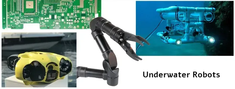
The exploration of underwater environments has always been a challenging yet captivating endeavor. From scientific research to infrastructure inspection, underwater detection robots play a crucial role. At the heart of these sophisticated machines lies the printed circuit board (PCB), the unsung hero that enables their functionality. Just as a nervous system controls the body, the PCB acts as the central nervous system of the robot, orchestrating the intricate dance of electronic components. But, how do you ensure reliability and performance in the face of immense pressure, corrosive saltwater, and unpredictable conditions? Zero One Solution Limited provides advanced PCB solutions for underwater detection robots, from design to manufacturing and assembly, we ensure your robots are ready to dive into the deep.
Introduction: The Critical Role of PCBs in Underwater Robotics
Printed Circuit Boards (PCBs) are the fundamental neural network of any modern electronic device, and in the demanding realm of underwater detection robots, their role transcends mere functionality—it is absolutely critical to mission success and longevity. Operating in an environment characterized by extreme pressure, corrosive saltwater, and fluctuating temperatures, the PCBs within these sophisticated machines must exhibit unparalleled reliability, durability, and signal integrity. A failure at the PCB level can lead to catastrophic system breakdowns, rendering multi-million dollar robotic assets inoperable and jeopardizing valuable data collection. Zero One Solution Limited, a veteran PCB solution provider with over a decade of specialization in rapid prototyping and one-stop services from design to assembly, stands at the forefront of engineering robust PCB solutions tailored specifically for the harsh and unforgiving underwater domain.
Understanding the Demands of Underwater Environments on PCBs
The operational efficacy of underwater detection robots hinges critically on their Printed Circuit Boards (PCBs). These delicate electronic components are subjected to one of the most hostile environments on Earth, demanding a profound understanding of the unique stresses imposed by deep-sea conditions. From crushing pressures to corrosive elements and fluctuating temperatures, every aspect of the underwater milieu poses a significant threat to conventional PCB performance and longevity. Overcoming these challenges requires specialized design, material selection, and manufacturing processes, ensuring the robot's ability to reliably collect and transmit vital data in its submerged habitat. The integrity of the PCB directly correlates with the success of the entire underwater mission.
Extreme Water Pressure Deep-sea environments exert immense hydrostatic pressure, which can lead to physical deformation or cracking of standard PCB substrates and components. This necessitates the use of high-strength, low-porosity materials and robust structural designs to prevent delamination or component failure under compression. For instance, at 1,000 meters depth, the pressure reaches approximately 100 atmospheres (1470 psi), requiring materials and enclosures capable of withstanding such forces without compromising electrical integrity. Specific attention must be paid to voids within the PCB and component packaging, as these can become points of failure under extreme pressure differentials.
Corrosive Saline Exposure Seawater, rich in salts and minerals, is a highly corrosive electrolyte. Direct or indirect exposure can lead to oxidation, short circuits, and material degradation of unprotected PCB traces, pads, and component pins. Advanced conformal coatings and hermetic sealing techniques are indispensable to create an impervious barrier against ion migration and chemical attack, preserving the circuit's functionality and preventing irreversible damage. Materials like gold plating on contacts offer superior corrosion resistance compared to tin or nickel.
Temperature Variations and Thermal Management Underwater temperatures can vary significantly, from near-freezing in abyssal plains to warmer conditions near hydrothermal vents. These fluctuations can induce thermal stress on PCBs, leading to material expansion and contraction, which may cause solder joint fatigue, component detachment, or substrate cracking over time. Effective thermal management, including optimized component placement for heat dissipation and selection of materials with matched Coefficients of Thermal Expansion (CTE), is crucial to maintain stability and prevent thermal runaway in active components. High-Tg (glass transition temperature) laminates are often preferred for their stability across wider temperature ranges.
Reliable Signal Transmission and EMI/EMC Maintaining signal integrity in an electromagnetically noisy and often confined underwater environment is paramount. Underwater robots operate complex sensor arrays, communication systems, and propulsion units, all generating electromagnetic interference (EMI). Furthermore, the unique dielectric properties of water can attenuate signals. PCB designs must incorporate meticulous impedance control, optimized routing, and effective electromagnetic compatibility (EMC) shielding to minimize crosstalk, ensure high-fidelity data transmission, and prevent external noise from disrupting critical operations. Ground planes and proper shielding are essential to mitigate interference in these challenging conditions.
Zero One Solution's Comprehensive PCB Design Services for Underwater Applications
PCB Design Software for Underwater Applications
Designing printed circuit boards (PCBs) for underwater applications demands a specialized approach, moving beyond conventional methodologies to address the unique and unforgiving challenges of subsea environments. Zero One Solution Limited, with its two decades of Silicon Valley expertise, offers comprehensive PCB design services specifically tailored for underwater detection robots. Our focus extends beyond basic circuit layout, encompassing critical considerations such as advanced material selection, optimized component placement, and strict adherence to relevant industry standards, ensuring the utmost reliability and performance in the most demanding marine conditions.
Material Selection: The Foundation of Underwater Durability The choice of PCB substrate and materials is paramount for underwater longevity. We leverage high-grade epoxy resins, known for their low water absorption and excellent dielectric properties, and explore advanced ceramic substrates for extreme pressure and temperature resilience. Encapsulation materials, coatings, and solder masks are carefully chosen to withstand saltwater corrosion, hydrostatic pressure, and temperature fluctuations, effectively forming an impenetrable barrier against environmental degradation.
Optimized Component Placement for Performance and Reliability Strategic component placement is crucial for both thermal management and signal integrity in underwater PCBs. Our design process prioritizes optimal heat dissipation, preventing localized hotspots that can compromise component lifespan. Furthermore, careful layout minimizes signal interference and electromagnetic compatibility (EMC) issues, which are exacerbated in enclosed, high-density underwater systems. This meticulous approach ensures stable and accurate data acquisition and processing.
Adherence to Stringent Industry Standards and Protocols Compliance with industry-specific standards is non-negotiable for underwater electronic systems. Zero One Solution adheres to relevant IPC standards (e.g., IPC-6012, IPC-A-610) for PCB performance and quality, alongside considering marine-specific certifications like DNV GL, ABS, or equivalent, where applicable. Our designs account for factors like shock and vibration resistance, ingress protection (IP ratings), and insulation requirements to guarantee operational integrity under harsh subsea conditions.
Design Aspect
Key Consideration
Benefit for Underwater Robots
Material Selection
Low water absorption, corrosion resistance
Prevents short circuits, extends operational life in saltwater
Protects electronics from water ingress and pressure
Design for Manufacturability (DFM)
Component accessibility, assembly ease
Reduces production costs, improves reliability of assembled board
Advanced Manufacturing Techniques for Robust Underwater PCBs
Specialized Epoxy Resin PCB
Crafting PCBs for the extreme depths of underwater environments demands a mastery of advanced manufacturing techniques that go far beyond standard production. Zero One Solution Limited employs a suite of specialized processes to ensure the unparalleled durability and reliability of our underwater PCBs, guaranteeing their performance under immense pressure, corrosive elements, and fluctuating temperatures. Our commitment to these sophisticated methods is what sets our solutions apart, providing the foundational robustness critical for any successful underwater detection robot.
Conformal Coating Application We utilize advanced conformal coatings, such as acrylic, silicone, urethane, and parylene, precisely applied to protect the PCB from moisture, chemicals, and extreme temperatures. These coatings form a protective barrier, preventing short circuits and corrosion in saltwater environments. Our process ensures uniform thickness and complete coverage, validated through meticulous inspection.
Encapsulation and Potting For ultimate protection, sensitive components and entire PCB assemblies are encapsulated using specialized resins. This process provides a robust, sealed barrier against water ingress and mechanical shock. We select materials with excellent dielectric properties and low water absorption rates, ensuring long-term insulation and structural integrity even under deep-sea pressures.
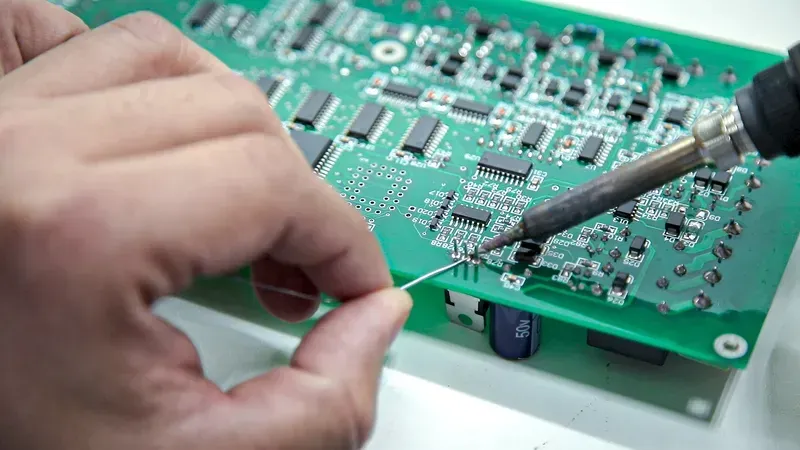
Precision Soldering and Interconnection Given the demanding operating conditions, the integrity of solder joints is paramount. We employ advanced soldering techniques, including vacuum reflow and selective soldering, to minimize voids and ensure strong, reliable interconnections. This meticulous approach prevents fatigue and failure caused by thermal cycling and vibrations encountered in underwater operations.
Manufacturing Technique
Primary Benefit for Underwater PCBs
Typical Application
Conformal Coating
Protection against moisture, corrosion, and electrical leakage
General PCB surface protection
Encapsulation/Potting
Superior water ingress prevention, mechanical shock resistance
Protection of critical modules and entire assemblies
Pressure Curing
Ensures material density and void-free encapsulation
High-pressure rated components and boards
Hermetic Sealing
Absolute environmental isolation
Sensors and sensitive electronic enclosures
Our rigorous quality control measures are integrated throughout the manufacturing process. This includes automated optical inspection (AOI) to detect subtle defects, X-ray inspection for internal solder joint integrity, and specialized pressure and leakage testing to simulate deep-sea conditions. Each PCB undergoes comprehensive validation, ensuring it meets the stringent performance and reliability standards required for underwater detection robotics. By integrating these advanced techniques, Zero One Solution Limited delivers PCBs that not only survive but thrive in the most challenging marine environments.
PCB Assembly and Testing for Underwater Detection Robots
PCB Assembly and Soldering Process
The robust performance of underwater detection robots hinges critically on the precise assembly and rigorous testing of their Printed Circuit Boards (PCBs). At Zero One Solution Limited, we understand that even the most meticulously designed PCB can fail without flawless assembly and comprehensive validation. Our advanced facilities and seasoned technicians ensure that every component is optimally placed and secured, followed by a multi-faceted testing regime that simulates the extreme conditions of the marine environment, guaranteeing unmatched reliability and functionality.
Precision Assembly for Subsea Resilience Achieving resilience in underwater PCBs starts with meticulous assembly. We employ automated pick-and-place machines for high precision and consistency, augmented by skilled manual assembly for complex or delicate components. Critical considerations include using low-void soldering techniques (e.g., vacuum reflow) to eliminate air bubbles that could compromise integrity under pressure, and precise component spacing to optimize thermal management and signal integrity within sealed enclosures. Our processes adhere strictly to IPC Class 3 standards for high-reliability electronic assemblies.
Specialized Soldering Techniques for Harsh Environments For underwater applications, traditional soldering may not suffice. We utilize specialized soldering techniques such as selective soldering and advanced wave soldering with specific flux formulations designed to enhance joint strength and corrosion resistance. Furthermore, we implement robust wire bonding and encapsulation of sensitive components, minimizing their exposure to moisture and physical stress, which is crucial for long-term operational stability in submerged conditions.
Comprehensive Environmental Stress Testing Our testing protocols extend far beyond basic electrical checks. Each assembled PCB undergoes a suite of environmental stress tests to simulate real-world underwater conditions. This includes accelerated life testing, thermal cycling (-40°C to +85°C) to identify material fatigue, and vibration testing to mimic operational stresses. These tests help to uncover potential weaknesses before deployment, ensuring the PCB's integrity against mechanical and thermal fluctuations.
High-Pressure Submersion and Leakage Testing A cornerstone of our validation process is high-pressure submersion testing. PCBs, often integrated into sealed enclosures, are subjected to hydrostatic pressures significantly exceeding their intended operational depth, typically up to 1000 meters or more, simulating deep-sea environments. This test rigorously checks for any structural weaknesses or sealing imperfections that could lead to water ingress. Concurrently, helium leak detection or vacuum decay tests are employed to detect even the minutest leaks in sealed components or enclosures.
Salt Spray and Corrosion Resistance Testing Given the corrosive nature of seawater, our testing includes rigorous salt spray testing (e.g., ASTM B117 standards). This evaluates the long-term resistance of the PCB's protective coatings, exposed components, and connectors to saline environments. PCBs are subjected to a fine mist of saltwater for extended periods, followed by visual inspection and electrical performance checks, ensuring that corrosion does not compromise signal integrity or power delivery over time.
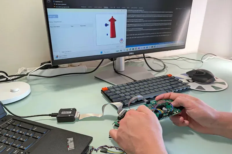
Functional and In-Circuit Testing (ICT) Beyond environmental resilience, we perform exhaustive functional testing to verify that the PCB operates precisely as designed under simulated loads. This includes simulating sensor inputs, actuator commands, and communication protocols. In-Circuit Testing (ICT) is also utilized to check for opens, shorts, resistance, capacitance, and other basic electrical parameters of individual components, ensuring every part is correctly placed and functioning within specifications. This two-pronged approach guarantees both physical integrity and electrical performance.
Case Studies: Zero One Solution's Success in Underwater Robotics PCB Projects
Underwater Robot PCB Testing
Zero One Solution Limited has a proven track record in delivering robust and reliable PCB solutions for the demanding field of underwater robotics. Our expertise in navigating the unique challenges of subsea environments has empowered numerous clients to bring their innovative underwater detection robots to life. These case studies highlight our commitment to excellence, rapid prototyping capabilities, and the custom-tailored approaches we employ to ensure project success, often exceeding stringent performance and reliability benchmarks.
Client
Project Type
Challenge
Zero One Solution's PCB Solution
Outcome
Oceanic Explorer Co.
Deep-Sea Imaging AUV
Extreme pressure (6,000m depth), high-resolution sensor integration, low power consumption.
Custom multi-layer PCB with high-Tg laminate, optimized impedance control for high-speed data, ultra-compact design, specialized hermetic sealing design collaboration.
Successful deployment of AUV in Mariana Trench; captured unprecedented geological data with minimal power drain and zero operational failures over extended missions. ROI significantly improved due to extended operational windows.
:Sub-Aqua Defence Ltd.
Autonomous Underwater Vehicle (AUV) for Maritime Security
High EMI/RFI interference from integrated sonar and communication systems, rapid deployment in varying water conditions, need for real-time data processing.
Rigid-flex PCB for signal integrity in dynamic environments, advanced EMI shielding techniques (ground planes, shielding layers), robust thermal management for embedded processors, rapid prototyping for iterative design refinement.
Enhanced signal-to-noise ratio in sonar data, improved real-time threat detection capabilities, faster mission deployment times by 30%, and significantly reduced maintenance downtime. Unit performed flawlessly in multiple high-stakes simulations.
:Marine Research Institute
Environmental Monitoring ROV Network
Prolonged exposure to corrosive saltwater, biofouling prevention, miniaturization for dense sensor arrays, long-term operational stability.
FR4 PCB with aerospace-grade conformal coating (parylene), custom-designed impedance matched traces for sensor accuracy, compact SMT component placement, integrated anti-corrosion features into the design specifications, collaborative material selection for bio-resistant properties.
Increased sensor data accuracy by 15% due to stable signal transmission; ROVs operated continuously for over 18 months without component degradation, leading to comprehensive long-term environmental datasets and reduced servicing costs by 40%.
The Future of Underwater Robotics and PCB Technology
Miniature Underwater Robot
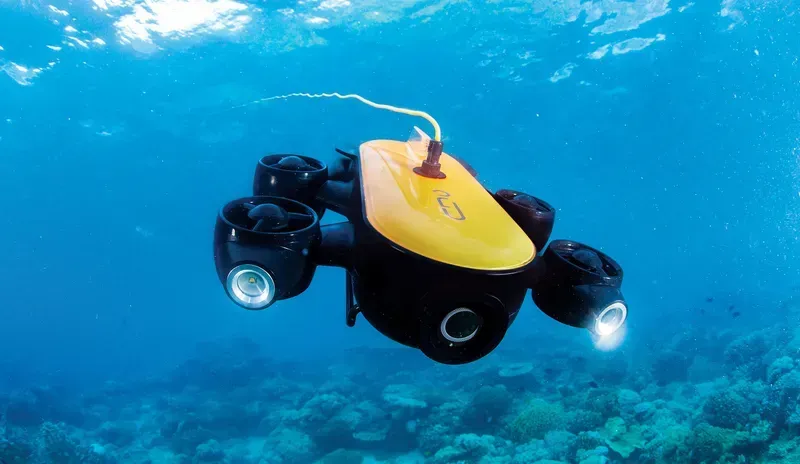
The relentless exploration of the underwater world is driving unprecedented innovation in robotics, directly shaping the evolution of PCB technology. As underwater detection robots become more sophisticated, demanding greater autonomy, multi-functionality, and extended operational lifespans, PCBs are evolving to meet these rigorous requirements. This symbiotic relationship pushes the boundaries of material science, circuit design, and manufacturing processes, ensuring that the electronic heart of these critical devices can withstand the most extreme subsea environments.
Miniaturization and High-Density Integration Future underwater robots will emphasize compact designs without sacrificing performance. This trend necessitates significant advancements in PCB miniaturization, including the development of micro-vias, thinner substrates, and higher component density. Integrating multiple functionalities onto a single, smaller board reduces the overall footprint and weight of the robot, which is crucial for enhanced maneuverability and extended mission durations in confined or deep-sea environments. Expect more System-in-Package (SiP) and Package-on-Package (PoP) solutions within PCB assemblies to achieve this.
Flexible and Stretchable PCBs Beyond traditional rigid boards, flexible and even stretchable PCBs are emerging as a game-changer for next-generation underwater robotics. These technologies enable PCBs to conform to irregular shapes, reducing spatial constraints and offering greater design freedom for novel robotic structures, such as biomimetic designs or soft robots. Flexible PCBs also enhance durability by distributing stress more evenly, which is vital for applications involving dynamic movements or high shock environments. This will be critical for robots designed for intricate inspection, manipulation, or long-term deployment on uneven seafloors.
Advanced Wireless Communication and Energy Transfer The future of underwater robotics will heavily rely on robust wireless communication and efficient energy transfer to reduce the need for tethered operations. PCBs will integrate advanced wireless transceivers, including acoustic modems and optical communication modules, optimized for underwater signal propagation. Furthermore, advancements in inductive charging and wireless power transfer directly to the robot's internal power systems, facilitated by specialized PCB coils and resonant circuits, will extend mission capabilities and simplify deployment and retrieval processes. This reduces external connection points, enhancing overall system reliability and waterproofing.
Enhanced Environmental Resilience and Material Science As robots venture into increasingly challenging hydrothermal vents or polar regions, PCBs will demand even greater resilience. This includes the development of novel substrate materials with superior thermal stability, chemical resistance, and dielectric properties under extreme pressures. Self-healing materials for protective coatings and embedded sensors for real-time environmental monitoring on the PCB itself will become standard, providing proactive maintenance and extending operational life in corrosive and high-pressure underwater conditions.
Why Choose Zero One Solution Limited for Your Underwater Robot PCB Needs?
Choosing the right PCB solution provider is paramount for the success of any underwater detection robot project, where reliability and performance are non-negotiable. Zero One Solution Limited stands as a beacon of excellence in this specialized field, offering unparalleled expertise and a proven track record in delivering robust PCB solutions tailored for the harshest marine environments. Our dedication to innovation, rapid prototyping, and unwavering quality assurance ensures that your underwater robotics initiatives are built on a foundation of superior electronic hardware.
Unrivaled Expertise in Harsh Environment PCBs With over a decade of experience, Zero One Solution Limited possesses deep domain knowledge in designing and manufacturing PCBs specifically for extreme conditions. Our engineering team understands the unique challenges of underwater applications, from high pressure and corrosive saltwater to temperature fluctuations and signal integrity demands. This specialized expertise translates into PCBs that are not just functional, but truly resilient and reliable in subsea operations, mitigating risks and ensuring mission success for your underwater robot PCB needs.
Advanced Technology and Manufacturing Capabilities We leverage state-of-the-art technology and advanced manufacturing processes to produce PCBs that meet the highest standards of durability and performance. This includes sophisticated material selection for water resistance and corrosion prevention, precision component placement, and protective measures like conformal coating and encapsulation. Our facilities are equipped with cutting-edge machinery for intricate multi-layer designs and rigorous testing protocols, ensuring every PCB can withstand the rigors of underwater deployment.
Rapid Prototyping for Accelerated Development In the fast-paced world of robotics, speed to market is a critical advantage. Zero One Solution Limited specializes in rapid prototyping, enabling quick iterations and adjustments to your PCB designs. This agile approach significantly reduces development cycles, allowing you to test and refine your underwater detection robot prototypes efficiently, ultimately accelerating your product's launch and securing a competitive edge. Our ability to swiftly move from concept to functional prototype is a cornerstone of our value proposition.
Comprehensive Quality Assurance and Reliability Quality and reliability are at the core of our operations. Every PCB manufactured for underwater applications undergoes stringent quality control and extensive testing, including pressure testing, leak detection, and salt spray exposure, to simulate real-world underwater conditions. Our commitment to ISO-certified processes and meticulous inspection ensures that each PCB delivered is free from defects and performs flawlessly under pressure, guaranteeing the long-term operational integrity of your underwater robots.
Strategic Global Presence and Supply Chain Headquartered in Shenzhen, China, and with a branch in Dubai, Zero One Solution Limited operates within a robust global PCBA supply chain network. This strategic positioning provides seamless access to premium components and resources, enabling efficient production and timely delivery worldwide. Our global footprint ensures that we can support your projects, regardless of location, offering responsive service and logistical advantages that streamline your procurement process for underwater robot PCB solutions.
Frequently Asked Questions (FAQs) about Underwater Robot PCBs
Addressing the unique challenges of underwater environments for printed circuit boards (PCBs) is crucial for the reliability and performance of underwater detection robots. This section answers frequently asked questions regarding the specialized PCB considerations for these demanding applications, from material selection to rigorous testing.
What are the primary challenges for PCBs in underwater detection robots? Underwater PCBs face significant challenges including extreme hydrostatic pressure, corrosive saline environments, wide temperature fluctuations, and the critical need for highly reliable signal integrity. These factors necessitate specialized materials and robust manufacturing processes to ensure long-term operational stability.
What types of materials are best suited for underwater robot PCBs? Optimal materials for underwater PCBs include high-grade epoxy resins (e.g., FR-4 variants with enhanced moisture resistance), ceramic substrates for high-frequency applications, and specialized laminates with low water absorption properties. Conformal coatings and potting compounds are also crucial for environmental protection.
How does Zero One Solution Limited ensure signal integrity in underwater PCB designs? Zero One Solution Limited employs meticulous design practices to maintain signal integrity, including impedance-controlled routing, careful consideration of trace lengths, strategic component placement to minimize crosstalk, and comprehensive electromagnetic compatibility (EMC) analysis. This is vital for accurate data acquisition and communication in noisy underwater environments.
What specific manufacturing processes enhance the durability of underwater PCBs? To enhance durability, Zero One Solution Limited utilizes advanced manufacturing processes such as vacuum lamination for void-free construction, precision drilling for accurate component placement, and specialized surface finishes for corrosion resistance. Multi-layer fabrication with optimized stack-ups further contributes to mechanical robustness.
What testing procedures are performed on underwater robot PCBs to ensure reliability? Reliability is assured through rigorous testing protocols, including hydrostatic pressure testing to simulate operational depths, salt spray testing to evaluate corrosion resistance, thermal cycling to assess performance across temperature extremes, and exhaustive functional testing to verify electrical performance under simulated environmental conditions. These tests validate the PCB's integrity before deployment.
In summary, the PCB is a vital component of any underwater detection robot, requiring careful consideration and expert design to ensure optimal performance and longevity. Zero One Solution Limited is dedicated to providing cutting-edge PCB solutions tailored to the unique challenges of underwater environments. By partnering with us, you gain access to our expertise in rapid prototyping, manufacturing, and assembly, empowering you to create innovative and reliable underwater robots. Contact us today to discuss your project and discover how our PCB solutions can help you dive deeper and achieve more in the underwater world. Let's work together to push the boundaries of underwater exploration and discovery.