Top Heavy Copper PCB Manufacturers: Powering High-Performance Electronics
2025.01.07
In the realm of advanced electronics, the demand for robust and efficient power delivery has never been greater. This is where heavy copper PCBs come into play, offering superior current carrying capacity and thermal management capabilities compared to standard PCBs. These specialized boards are critical in high-power applications, such as automotive, industrial control systems, and renewable energy devices. Understanding the capabilities of different heavy copper PCB manufacturers is crucial for success in these demanding fields. This article delves into what defines heavy copper PCBs, the advantages they offer, and how to choose the right manufacturer. Let’s explore the landscape of these specialized component makers.
What Are Heavy Copper PCBs?
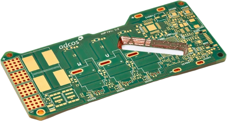
Heavy Copper PCB
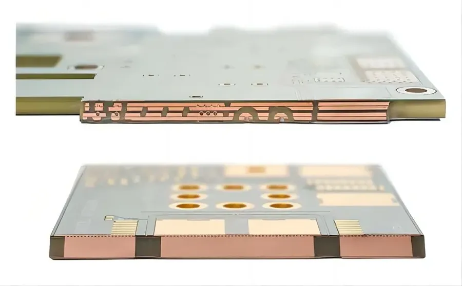
Heavy copper PCBs are characterized by copper layers that are significantly thicker than those found in standard printed circuit boards. This increased copper thickness, typically ranging from 3 oz to 20 oz per square foot (or more), enables the boards to handle higher current loads and improve thermal management, crucial for high-power applications. These PCBs are not merely about thicker copper; they often require specific manufacturing techniques and materials to maintain performance and reliability.
The key characteristics of heavy copper PCBs include:
Copper Thickness The most defining characteristic, with copper layers typically ranging from 3 oz/ft² to 20 oz/ft² or even more in specialized applications. Standard PCBs use 1 oz/ft² or less.
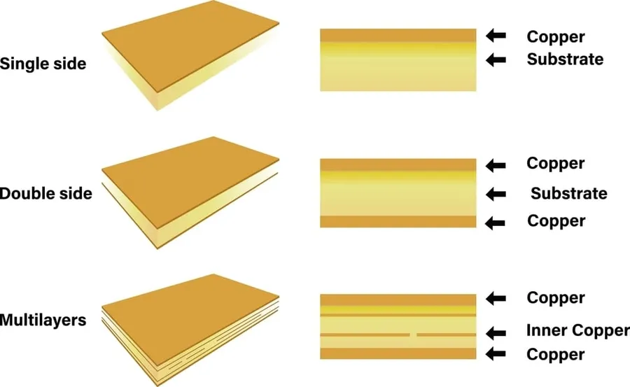
Layer Construction Heavy copper PCBs can be single-layer, double-layer, or multi-layer boards, with each layer having the specified heavy copper thickness. This may require specialized bonding and lamination processes.
Material Selection The substrate material used can be of standard FR-4 or high-performance materials such as Aluminum, Polyimide, or PTFE, with greater attention to thermal conductivity and coefficient of thermal expansion (CTE) matching. Material selection is often directly impacted by the operational environment and high-current/thermal demands.
Typical Applications Heavy copper PCBs are predominantly found in applications requiring high current, superior heat dissipation, and enhanced mechanical robustness, including power electronics, automotive systems, industrial controls, and renewable energy systems.
Advantages of Using Heavy Copper PCBs
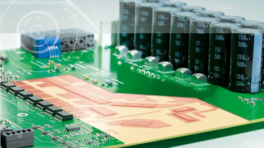
High Current PCB
Heavy copper PCBs offer distinct advantages over standard PCBs, primarily due to their thicker copper layers, which directly translate to enhanced performance in demanding applications. These advantages include superior current carrying capacity, improved thermal management, and reduced electrical resistance.
Enhanced Current Carrying Capacity Thicker copper layers allow heavy copper PCBs to handle significantly higher currents compared to standard PCBs. This is crucial in power electronics, where high current loads are common. A thicker copper trace has a lower resistance, allowing it to carry more current without overheating. The current-carrying capacity increases nearly proportionally to the cross-sectional area of the copper trace.
Improved Thermal Performance Heavy copper PCBs excel in thermal management due to their increased copper mass, which acts as a natural heatsink. This improved thermal conductivity allows for better heat dissipation, reducing the risk of component failure due to overheating. The enhanced thermal performance also allows for higher operating temperatures without degradation of performance.
Reduced Electrical Resistance The thicker copper traces in heavy copper PCBs offer significantly lower electrical resistance, leading to reduced power losses and more efficient operation. This reduction in resistance translates directly into reduced voltage drops, which is essential for sensitive electronic circuits that require stable power delivery. This increased efficiency also reduces wasted heat which also contributes to improved thermal performance.
Increased Durability and Mechanical Strength The increased copper thickness provides the PCB with greater mechanical robustness, making it more resistant to damage from thermal cycling and physical stress. This makes them suitable for harsh operating environments, such as those found in automotive and industrial applications.
Key Considerations When Selecting a Heavy Copper PCB Manufacturer
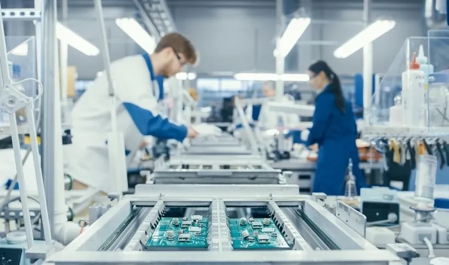
PCB Manufacturing Facility
Selecting a heavy copper PCB manufacturer requires careful evaluation of several critical factors to ensure the final product meets the performance and reliability requirements of your application. These factors encompass manufacturing capabilities, certifications, and the level of design support provided.
Manufacturing Capabilities A manufacturer's capabilities directly influence the quality and feasibility of your heavy copper PCB. Critical aspects include the maximum copper thickness they can achieve, which typically ranges from 3 oz to 20 oz (or even higher), depending on the manufacturer's equipment and expertise. They must also support your required board size and maintain tight tolerances during the manufacturing process, which is particularly challenging with thicker copper layers.
Certifications and Quality Standards Certifications such as ISO 9001 and UL are crucial indicators of a manufacturer’s commitment to quality and process control. ISO 9001 ensures consistent quality management systems are in place, while UL certification demonstrates the manufacturer’s ability to produce PCBs that meet specific safety and performance standards. These certifications provide confidence in the reliability and consistency of the PCBs produced.
Design Support and Engineering Expertise Beyond manufacturing, a reputable heavy copper PCB manufacturer should offer robust design support services. This includes design-for-manufacturability (DFM) analysis, which helps identify potential issues before production, and engineering expertise to assist with material selection, layer stack-up optimization, and thermal management strategies. Access to experienced engineers can significantly reduce design iterations and enhance overall project success.
Heavy Copper PCB Manufacturing Processes
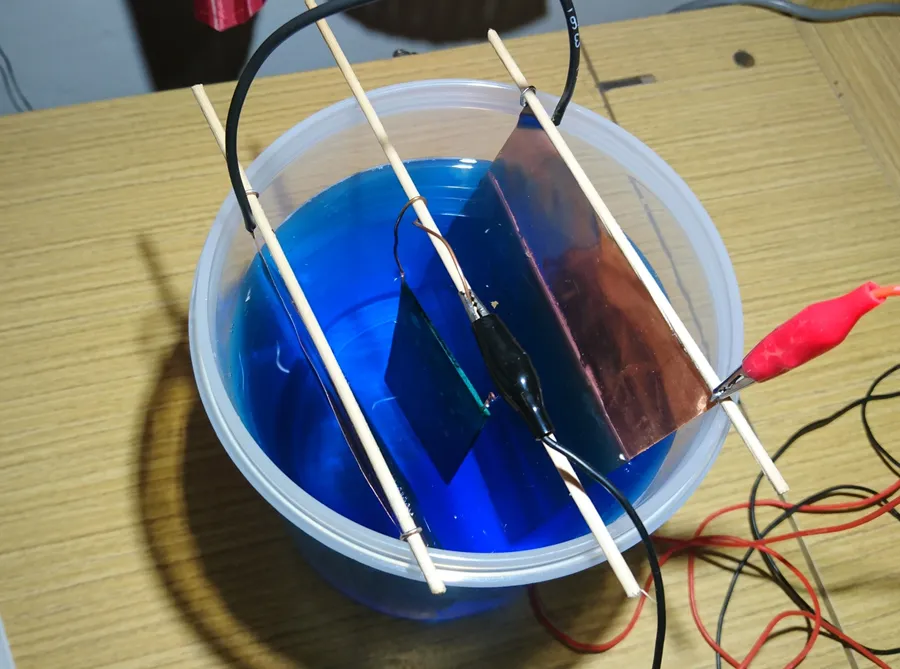
PCB Electroplating
Manufacturing heavy copper PCBs demands meticulous control over plating, etching, and lamination processes to accommodate the increased copper thickness. These processes are critical for achieving the desired electrical and thermal performance while maintaining the integrity of the board.
Here's a breakdown of the key manufacturing steps:
1. Copper Plating The process begins with the electroplating of copper onto the substrate, which could be a dielectric material such as FR-4. For heavy copper PCBs, a thicker layer of copper is deposited using a specialized plating process. This plating process demands precise control of current density, plating time, and chemical composition to ensure a uniform and consistent copper layer across the board.
2. Imaging and Etching Once the copper plating is complete, a photoresist is applied and imaged to define the circuit pattern. After the imaging process, the exposed copper is etched away using chemical solutions. The precision of this etching process is paramount in heavy copper PCBs, as variations in etching can significantly alter the trace widths and clearances, affecting both electrical performance and impedance control.
3. Lamination Multiple layers of the circuit board, each with its patterned copper layers, are laminated together under heat and pressure, using a prepreg bonding material. For heavy copper PCBs, the thickness of the copper layers and the overall board requires specific lamination parameters to ensure secure bonding and prevent layer separation or delamination.
4. Drilling and Through-Hole Plating After lamination, holes for vias and component mounting are drilled. These holes are then plated to create electrical connections between layers. This step also needs tight control to ensure proper via wall thickness and connectivity.
5. Final Surface Finish The final surface finish, such as ENIG (Electroless Nickel Immersion Gold) or HASL (Hot Air Solder Leveling), is applied to protect the copper and provide a solderable surface for component mounting.
Applications of Heavy Copper PCBs
Heavy Copper PCB Applications
Heavy copper PCBs, characterized by their thicker copper layers, are indispensable in applications requiring high current carrying capacity, efficient heat dissipation, and robust electrical connections. These boards extend beyond standard circuit boards and are vital for power-intensive and environmentally demanding applications.
Power Electronics Heavy copper PCBs are fundamental in power converters, inverters, and motor drives where high current levels and thermal management are crucial. The increased copper thickness allows for more efficient power transmission and heat dissipation, ensuring the reliability of power electronic systems.
Automotive Systems Within the automotive sector, these PCBs are used in electric vehicle (EV) power train systems, including battery management systems (BMS) and power distribution modules. The ability to withstand high operating temperatures and current loads is essential for the demanding environment of automotive applications.
Industrial Equipment Heavy copper PCBs are crucial in industrial equipment such as high-power machinery, welding equipment, and industrial automation systems. The robustness and durability of these PCBs ensure the reliable operation of heavy-duty industrial applications.
Renewable Energy Sectors In renewable energy applications, heavy copper PCBs are vital in solar inverters, wind turbine power converters, and energy storage systems. These boards facilitate the efficient conversion and storage of energy, supporting the growth of renewable energy technologies. The reliability and durability of these PCBs under varied environmental conditions are critical for these applications.
High-Power LED Lighting Heavy copper PCBs are also ideal for high-power LED lighting systems where efficient heat management is paramount to prevent overheating and ensure the longevity of LEDs.
Aerospace and Defense In aerospace and defense applications, heavy copper PCBs are used in radar systems, power supplies, and high-reliability electronic equipment requiring dependable performance under extreme conditions.
Frequently Asked Questions About Heavy Copper PCBs
This section addresses common questions about heavy copper PCBs, providing clarity on their specifications, cost implications, design considerations, and production timelines. Understanding these aspects is crucial for anyone considering using heavy copper PCBs in their electronic designs.
What is considered 'heavy copper' in a PCB? Heavy copper PCBs are characterized by copper layers that are 3 oz (105µm) or more. Standard PCBs typically have copper weights of 1 oz (35µm) or less. The increased copper thickness enhances the board's current-carrying capacity and thermal management capabilities.
How thick can the copper be in a heavy copper PCB? While 3 oz is the starting point for 'heavy copper,' manufacturers can produce PCBs with copper weights up to 20 oz (700µm) or even more in specialized cases. The maximum thickness a manufacturer can achieve depends on their equipment and processes.
What are the advantages of using heavy copper PCBs? Heavy copper PCBs offer several advantages, most notably superior current-carrying capacity, enabling them to handle higher power levels. They also feature improved thermal management, which helps dissipate heat more effectively and can lead to lower operating temperatures and increased reliability. Additionally, they often have lower electrical resistance, minimizing power losses and signal degradation.
Are heavy copper PCBs more expensive to produce? Yes, heavy copper PCBs typically cost more than standard PCBs due to the increased material usage and the more demanding manufacturing processes needed to handle the thicker copper. The cost also varies depending on the copper thickness, layer count, and required tolerances.
What are the typical applications for heavy copper PCBs? Heavy copper PCBs are widely used in applications requiring high power and reliability, such as power converters, power inverters, automotive electronics, industrial control systems, high-power LED lighting, and renewable energy systems. Their robust performance makes them suitable for these demanding environments.
What design considerations are important for heavy copper PCBs? Designing heavy copper PCBs requires careful planning to address challenges like increased etching times, tighter tolerance controls, and potential issues with component placement due to the thicker copper. Attention should be paid to thermal vias for heat dissipation and proper pad design to ensure reliable solder joints. The designer should work closely with the manufacturer early in the process.
What are typical lead times for heavy copper PCB production? Lead times for heavy copper PCBs can be longer than those for standard PCBs due to the more complex manufacturing process. Production times can vary widely based on the copper thickness, layer count, specific manufacturer capabilities and the overall complexity of the design. For accurate lead times, it's best to consult directly with potential manufacturing partners.
Comparing Heavy Copper PCB Manufacturers: Capabilities and Specializations
Different Types of PCBs
Selecting the right heavy copper PCB manufacturer is crucial for ensuring the performance and reliability of your high-power electronic devices. This section provides a comparative overview of leading manufacturers, focusing on their copper layer capabilities, specializations, and typical lead times. This comparison allows for a more informed decision-making process based on specific project requirements.
Manufacturer
Maximum Copper Thickness (oz)
Specializations
Typical Lead Time
Certifications
Manufacturer A
10
High-layer count PCBs, Automotive applications
2-3 weeks
ISO 9001, UL
Manufacturer B
20
Power electronics, Metal core PCBs
3-4 weeks
ISO 14001, IPC-A-600
Manufacturer C
15
Renewable energy, High current boards
2-3 weeks
ISO 9001, ISO 13485
Manufacturer D
12
Industrial equipment, Advanced materials
2-4 weeks
ISO 9001, UL, RoHS
Manufacturer E
8
Flex PCBs, Complex geometries
3-5 weeks
ISO 9001, AS9100
Cost Factors for Heavy Copper PCB Production
The cost of producing heavy copper PCBs is influenced by several interconnected factors, primarily driven by the increased material usage and the more complex manufacturing processes required. Understanding these factors is crucial for accurate budgeting and project planning.
Copper Thickness The primary cost driver is the thickness of the copper layer. Increased copper weight means more material consumption, which leads to higher raw material costs and longer plating times. For example, a 4 oz copper PCB will inherently cost more than a standard 1 oz PCB due to the increased copper needed for manufacturing.
Board Complexity The complexity of the PCB design significantly impacts production costs. This includes the number of layers, via density, trace width and spacing. Intricate designs require more precision and can result in lower yields and longer fabrication times, increasing the overall cost. High-layer-count PCBs, for example, require more processing steps and higher-precision alignment.
Production Volume Economies of scale play a crucial role. Larger production runs usually result in lower per-unit costs due to optimized setups and reduced waste. Smaller volumes may incur higher costs due to setup and tooling charges being spread over fewer boards. PCB manufacturers frequently offer volume discounts. Prototype orders are typically significantly more expensive on a per-unit basis.
Board Size and Dimensions Larger board sizes require more raw material and may require specialized equipment for handling, both of which will increase production costs. The dimensions of the PCB also influence how many boards can be produced per panel, which can further impact manufacturing efficiency and overall cost.
Surface Finish The chosen surface finish impacts costs, with some options like gold plating being more expensive than others such as HASL or ENIG. The choice of surface finish must be suitable for the application requirements and will contribute to the overall price of the PCB.
Material Selection The selection of substrate materials, particularly for high-performance and high-temperature applications, influences cost. Specialty materials with improved thermal or electrical properties can significantly increase the cost compared to standard FR-4 material. Factors such as material availability and specific performance needs must be taken into account.
Testing and Quality Control Rigorous testing and quality control processes are crucial to ensure reliability, especially for heavy copper PCBs used in demanding environments. These additional testing steps contribute to the overall costs of the boards, but they guarantee the quality and performance of the final product.
Future Trends in Heavy Copper PCB Technology
The field of heavy copper PCB technology is continuously evolving, driven by the increasing demands of high-performance electronics. Emerging trends point towards the adoption of advanced materials, increased copper weights, and the seamless integration of PCBs with advanced technologies like embedded components, aiming for enhanced performance and reliability.
Advanced Materials Research is actively exploring materials with higher thermal conductivity and improved mechanical properties. These new substrates aim to manage the heat generated by high-current applications more efficiently while ensuring better structural integrity.
Higher Copper Weights The push for higher current-carrying capabilities is driving the development of PCBs with even thicker copper layers. This enhances performance in power electronics and reduces the risk of circuit failures due to overheating.
Integration with Embedded Components The integration of embedded components within the PCB structure aims to improve space utilization and reduce the overall size of electronic devices. This offers opportunities for more compact and efficient electronic systems.
Advanced Manufacturing Techniques Techniques such as additive manufacturing, also known as 3D printing, are being explored for their potential to produce highly customized heavy copper PCBs with complex geometries. This enables more flexibility in design and faster prototyping.
Sustainability and Eco-Friendly Materials There is a growing focus on using more sustainable and eco-friendly materials in the manufacturing process. This is in line with the global push for more responsible and environmentally conscious production of electronic devices.
Choosing the right heavy copper PCB manufacturer is essential for ensuring the reliability and efficiency of your high-power electronic applications. By understanding the key aspects of heavy copper PCBs and the capabilities of various heavy copper pcb manufacturers, you can secure a partnership that delivers high-quality, performance-driven boards. As technology advances, the demand for even more robust solutions will only grow. Selecting a manufacturer with proven experience and future-focused innovation is crucial in this ever-evolving space. The ability of heavy copper pcb manufacturers to innovate and meet stringent requirements will be a driving factor in the development of cutting edge electronics.