Ultimate Guide to Low Cost PCB Prototypes: From Design to Delivery
2025.01.04
In today's fast-paced tech world, rapid prototyping is crucial, and PCB prototypes are at the heart of hardware innovation. Securing a low cost PCB prototype is not just about saving money; it’s about enabling faster iteration and getting innovative products to market more efficiently. This article breaks down how to navigate the world of PCB prototyping on a budget, offering practical advice and comparing top manufacturers to help you make informed decisions.
Understanding PCB Prototype Costs: Key Factors
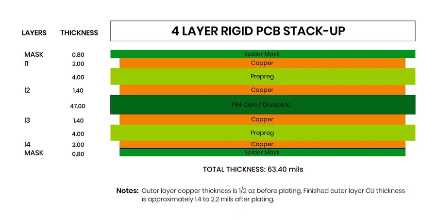
PCB Layer Stack Up
The cost of a PCB prototype is determined by a complex interplay of factors that span design parameters to manufacturing choices. A thorough understanding of these factors is critical for cost optimization and ensuring the budget stays within the defined limits for prototype development. Core determinants include board dimensions, the complexity of layer configurations, the choice of materials, the volume of the production run, and the tolerance requirements. Additionally, lead-time and shipping can also impact the total expenditure. Optimizing each element through deliberate design and judicious manufacturer selection is key to reducing expenditure.
Factor
Description
Impact on Cost
Optimization Strategies
Board Size
The physical dimensions of the PCB.
Larger boards require more material and processing, increasing cost.
Minimize board dimensions while still accommodating all necessary components and functionality.
Layer Count
The number of conductive layers within the PCB stack-up.
More layers increase manufacturing complexity and cost.
Use the minimal number of layers that meet the circuit's routing requirements.
Material Selection
The type of substrate material used (e.g., FR-4, CEM-1).
High-performance materials often come with higher costs.
Select materials based on performance requirements; where possible, consider more affordable alternatives without sacrificing functionality.
Production Volume
The quantity of PCBs being produced.
Larger volumes often benefit from economies of scale, reducing per-unit cost.
Consolidate orders with other projects or plan for future needs to increase volume and lower cost.
Lead Time
The time required to manufacture the boards.
Expedited lead times typically incur higher charges.
Plan ahead and use standard lead times where possible.
Tolerance Requirements
The precision with which the PCB must be manufactured
Tighter tolerance requirements increase manufacturing complexity and cost.
Select the minimum tolerance requirements suitable for your designs needs
Shipping Costs
The cost of delivering the finished PCBs
Shipping expenses are tied to location and speed, often impacting low volume orders.
Combine orders, and use standard shipping methods where possible.
Design Strategies for Low Cost PCB Prototypes
PCB Component Placement
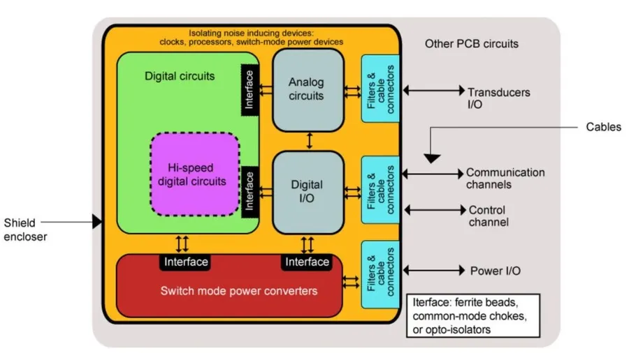
Effective PCB design is paramount in reducing prototype costs without compromising functionality. By carefully considering layout, component selection, and manufacturing constraints, designers can significantly impact the final price of their prototypes. This section delves into specific design strategies to minimize expenses while maintaining high-quality performance.
Optimized Board Layout A well-planned board layout minimizes the need for complex routing, which can reduce manufacturing costs. Aim for dense component placement with minimal spacing while avoiding unnecessarily complex shapes.
Minimizing Trace and Space Widths While it may seem counterintuitive, using the minimum acceptable trace width and spacing for signal integrity can reduce material use, and consequently, manufacturing costs. However, be sure to comply with your manufacturer's capabilities.
Standardized Component Choices Choosing commonly available, standard components significantly lowers costs due to their availability and competitive pricing. Consider using readily available components instead of less common ones which might have higher prices and longer lead times.
Through-Hole Component Usage Utilizing through-hole components for non-critical parts can often be more economical than Surface Mount Technology (SMT), especially in low volume prototyping. Through-hole components are generally less expensive, and can be easily placed by hand in low quantity production runs.
Panelization When producing multiple boards, consider panelizing them. Panelization allows for multiple PCBs to be produced in a single run, reducing costs by more effectively using the manufacturing area, and usually results in better overall costs.
Single-Sided Designs For simple circuits, using single-sided PCB designs will always be cheaper and less complex than double-sided or multilayer PCBs. It reduces manufacturing time and material requirements.
Design Consideration
Impact on Cost
Best Practice
Board Layer Count
Higher layers increase cost
Use the minimum number of layers needed
Board Size
Larger boards cost more
Optimize for compact layouts
Trace Width and Spacing
Tighter tolerances increase cost
Use the largest possible based on design constraints
Component Type
Surface mount components more expensive
Use through-hole where possible
Component Availability
Rare parts can increase costs
Use readily available components
Choosing the Right PCB Manufacturer: A Comprehensive Comparison
PCB Manufacturing Facility
Selecting the appropriate PCB manufacturer is crucial for achieving cost-effective prototyping. Several manufacturers specialize in low-cost PCB prototype services, each with unique strengths in pricing, turnaround times, and features. A comparative analysis is essential to identify the best fit for specific project requirements.
Manufacturer
Starting Price (USD)
Turnaround Time (Days)
Min Order Quantity
Layer Count Options
Special Features
JLCPCB
2
2-7
5
1-6
Wide range of colors, assembly services, low cost
PCBWay
5
3-8
5
1-12
Stencil service, advanced material options
Seeed Studio
5
4-10
1
1-6
Open Source Hardware Focus, one stop service
OSH Park
5
10-12
3
2
High-quality finish, shared panelization
PCBGOGO
5
3-7
1
1-14
Advanced PCB technologies, assembly service
PCB Unlimited
Varies
Varies
1
1-30
Wide range of material and layer options
The $1 PCB Prototype Myth: Understanding Promotional Offers
PCB Prototype
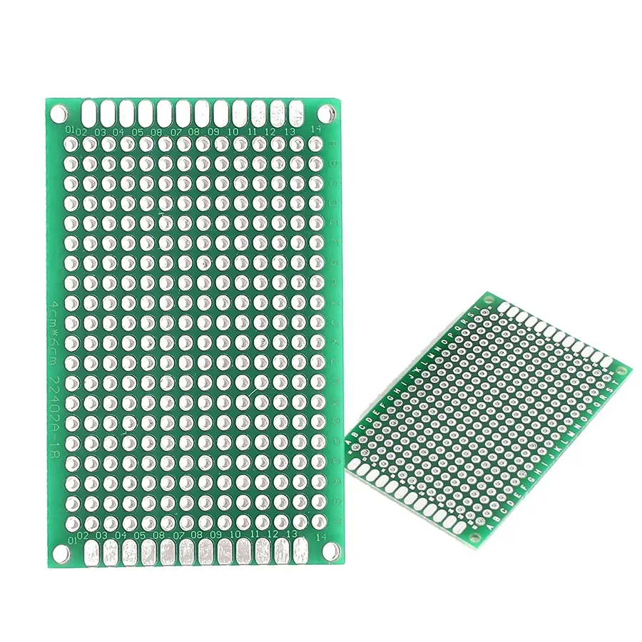
The allure of $1 PCB prototype promotions is strong, often serving as an entry point for new users and a marketing tool for manufacturers. While these offers can provide significant savings, it's crucial to understand their inherent limitations and potential additional costs to leverage them effectively.
These promotions, while seemingly straightforward, usually come with specific terms and conditions that can greatly influence their actual cost and suitability for different projects. It's essential to investigate these conditions thoroughly before committing to an order.
Limited Quantity Promotional offers often apply to a limited number of PCBs, typically ranging from 1 to 5 units. This is ideal for initial prototyping but may not cover the needs of larger projects or iterations.
Restricted Board Specifications The offer might be limited to specific board sizes, layer counts (often two layers), materials (typically FR-4), and minimum trace widths and clearances. Deviating from these specifications will usually incur additional costs.
Standard Finish Most $1 PCB promotions include a standard surface finish, like HASL (Hot Air Solder Leveling). Upgrading to ENIG (Electroless Nickel Immersion Gold) or other finishes typically involves extra charges.
Delivery Time Promotional orders can sometimes have longer lead times compared to standard orders. Be sure to check the estimated manufacturing and shipping duration. Also, sometimes promotional orders are shipped via economical shipping options with longer delivery times.
Additional Charges Beyond the initial $1 cost, be aware of added expenses for shipping, tooling fees (if applicable), and any optional services not included in the promotion, such as design rule checks, stencil creation, or panelization.
Targeted Audience These promotions are generally aimed at first-time users. Repeat orders or bulk manufacturing may not qualify for the promotional pricing.
To maximize the value of $1 PCB prototype offers, ensure your design aligns with the specified parameters, and plan ahead to mitigate potential hidden costs. Carefully consider the trade-offs between price and performance before finalizing your choice.
Optimizing Shipping Costs for Low Cost PCB Prototypes
PCB Shipping Package
Minimizing shipping expenses is crucial for maintaining the 'low cost' aspect of PCB prototypes, especially for smaller production runs. Strategic planning and understanding shipping logistics can significantly reduce the overall project cost.
Several key strategies can be employed to reduce shipping costs:
Consolidate Orders Whenever possible, combine multiple PCB prototype orders into a single shipment. This leverages economies of scale, reducing the cost per board.
Strategic Scheduling Align prototype production schedules with the manufacturer's production cycles to potentially benefit from lower, consolidated shipping rates.
Choose Cost-Effective Shipping Methods Select economy or standard shipping options rather than expedited services, unless project timelines absolutely require faster delivery. Consider various shipping partners, comparing price against delivery time.
Plan for Longer Lead Times By allowing extended lead times, the use of more economical and slower shipping methods becomes a feasible option.
Local Manufacturing If feasible, choose a local manufacturer to minimize or eliminate shipping costs. Also, consider the cost of material procurement and any manufacturing overheads, and include it in your calculations.
Negotiate with Suppliers For consistent, high volume projects, negotiate shipping rates with your manufacturer. In the long-run, it is beneficial to secure a stable and discounted rate.
By systematically considering these options, you can significantly reduce shipping expenses and keep your low-cost PCB prototype projects truly cost-effective.
PCB Material and Finish Options for Budget-Conscious Projects
FR4 PCB Material
The selection of PCB materials and surface finishes significantly influences the overall cost of a PCB prototype. For budget-conscious projects, it is essential to understand the trade-offs between cost and performance to make informed decisions. This section explores cost-effective alternatives to standard materials like FR-4 and various finish options.
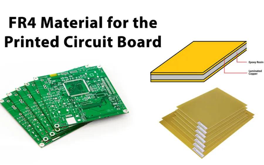
FR-4 is the most commonly used material for PCB production due to its good electrical insulation, mechanical strength, and relatively low cost. However, for less demanding applications, alternative materials like CEM-1 can offer further cost reductions. The table below provides a comparison of these two material types and considerations regarding their use:
Material Type
Cost
Properties
Typical Applications
Considerations
FR-4
Moderate
Good electrical and mechanical properties, flame retardant
Most general-purpose PCBs
Standard choice, good balance of cost and performance
CEM-1
Low
Paper-based composite, suitable for single-layer and simple double-layer boards
Low-cost electronics, non-critical applications
Less durable than FR-4, not recommended for high-stress conditions
PCB surface finishes provide protection from oxidation and enhance solderability. Common surface finishes, including their cost and suitability for low-cost PCB prototypes, are outlined below:
Surface Finish
Cost
Solderability
Shelf Life
Typical Applications
Considerations
HASL (Hot Air Solder Leveling)
Low
Good
Short to moderate
General-purpose prototypes, suitable for manual soldering
Lead or lead-free options available, can be uneven surface
Cost-sensitive applications, often used with reflow soldering
Environmentally friendly but requires careful handling
For budget-constrained projects, HASL is typically the most economical choice, particularly for through-hole components and larger pads. OSP is also a low-cost option, but its short shelf-life may impact the production time. ENIG provides excellent performance and reliability but comes at a higher cost.
Selecting the right PCB material and finish depends on specific project requirements, manufacturing capabilities, and budget constraints. While FR-4 remains a reliable standard, exploring alternative materials like CEM-1 and surface finishes such as HASL or OSP can provide cost-effective solutions for low-cost PCB prototypes.
Frequently Asked Questions About Low Cost PCB Prototypes
Navigating the landscape of low-cost PCB prototyping can raise numerous questions. This section addresses common queries, providing clear and concise answers to help you make informed decisions and optimize your prototyping process.
What is the typical cost of a PCB prototype? The cost of a PCB prototype varies significantly based on factors such as board size, layer count, material, finish, and the manufacturer. Simple, small, single or double-layer boards can be produced for under $5, while complex multi-layer boards with specialized materials can cost hundreds of dollars. It's crucial to get specific quotes based on your design requirements.
What are the cheapest methods for producing a PCB prototype? The cheapest methods involve using standardized designs, minimizing board size, opting for fewer layers (single or double-sided), selecting cost-effective materials like FR-4, and choosing basic finishes like HASL (Hot Air Solder Leveling). Additionally, ordering through manufacturers specializing in low-cost prototypes, like JLCPCB, can offer significant savings. Batching orders with others may also be an option if your schedule permits.
What are some budget-friendly PCB finish options? HASL (Hot Air Solder Leveling) is generally the most cost-effective finish option. It provides good solderability and is suitable for most applications. However, it is not ideal for fine pitch or fine detail. ENIG (Electroless Nickel Immersion Gold) is more expensive but provides better planarity and oxidation resistance. If cost is a major concern, and your design can tolerate it, HASL is usually preferred.
How can I start the process of creating a PCB prototype from scratch? The initial steps involve designing your schematic and board layout using EDA software (e.g., Eagle, KiCad, Altium). Next, generate Gerber files, which are the standard files required by PCB manufacturers. Choose a manufacturer that suits your budget and project needs, upload your Gerber files, select your options, and place your order. Be sure to review the manufacturer’s design rules and guidelines and confirm that your designs meet their requirements to minimize potential delays.
How much does a PCB prototype cost if I order a small batch? Ordering a small batch, instead of single boards, can significantly reduce the per-unit cost. Many manufacturers offer bulk discounts, and batching a few boards, especially if the boards are small, is usually more economical than ordering single boards. You still have to account for the setup costs, but after the first few boards, the cost per board goes down. The more boards you order at once, the cheaper the prototype cost becomes. Consider ordering multiple boards to share with colleagues to further bring down costs.
What are the primary cost drivers for PCB prototypes? The primary cost drivers include the board size, the number of layers (single, double or multi-layer), material selection, the chosen surface finish (HASL, ENIG, etc.), and the volume of the order. Other factors such as special milling requirements, via types, and whether you are using standard or specific impedance traces can also influence the price. Optimizing these factors can lead to substantial cost savings.
What is the impact of material selection on PCB prototype cost? The most commonly used material for PCBs is FR-4, which is typically cost-effective and versatile for general-purpose applications. However, higher performance materials like Rogers or polyimide can increase the cost significantly. For low cost prototypes, FR-4 is almost always the best choice. CEM-1, while less common, can be a suitable option for applications that have lower performance requirements and may be even more cost-effective than FR-4.
Avoiding Common Pitfalls and Hidden Costs in Low Cost PCB Prototyping
Navigating the landscape of low-cost PCB prototyping requires vigilance to avoid common pitfalls that can inflate costs and delay projects. Meticulous planning and informed decision-making are crucial to ensure your project stays within budget and meets the required specifications.
Inaccurate Design Files Submitting incomplete or incorrect Gerber files is a primary cause of delays and additional costs. Thoroughly check all design files and perform a design rule check (DRC) before submission. Ensure all layers are correctly aligned and all necessary information such as drill files are included.
Misunderstanding Manufacturer Capabilities Not all manufacturers offer the same capabilities. Verify the manufacturer's minimum trace width, spacing, drill hole sizes, and layer count limitations before designing your board. Designs exceeding these limitations will often result in added charges or design revisions.
Ignoring Minimum Order Quantities (MOQs) Many low-cost manufacturers have minimum order quantities. If your project only requires a small number of prototypes, you may have to order extra boards or pay extra. Factor this into your cost analysis and consider grouping prototypes together to reach the MOQ.
Unexpected Tooling and Setup Costs Be aware of setup fees for new designs or specific manufacturing options such as custom panelization. Tooling costs can sometimes make a small batch of prototypes more expensive on a per-board basis. Choose standard panelization to save costs if possible.
Component Sourcing Delays Component availability can fluctuate, and some manufacturers may not offer component assembly. If you choose to assemble the components yourself, factor in potential lead times and ensure the components are readily available to avoid holding up the production schedule.
Rushing the Design and Review Process Failing to adequately review the design before ordering prototypes is a common source of errors. Take the time to carefully review every aspect of the design and correct any mistakes before submitting your files for manufacture. This can save time, money and frustration in the long run.
Underestimating Shipping and Customs Fees Shipping costs are usually not included in the initial pricing. Be sure to factor in both shipping expenses and potential customs fees, especially when importing from overseas manufacturers. Consider consolidating orders or using efficient shipping methods to reduce costs.
Future Trends in Low Cost PCB Prototyping
Flex PCB
The landscape of low-cost PCB prototyping is continuously evolving, driven by technological advancements and increasing automation. These changes promise to further reduce costs, improve turnaround times, and enhance the capabilities available to designers, particularly hobbyists and small businesses.
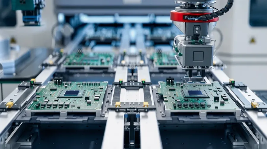
Increased Automation in Manufacturing Robotics and automated systems are becoming more prevalent in PCB manufacturing. This increased automation leads to higher throughput, reduced labor costs, and improved precision, ultimately lowering the price per board.
Advanced Manufacturing Techniques Emerging technologies like inkjet printing and laser direct structuring are poised to disrupt traditional manufacturing methods. These techniques offer the potential for faster and more flexible production, reducing costs and waste.
Improved Materials Science Ongoing research in materials science is leading to the development of new substrates and laminates that offer improved performance at lower costs. These materials may also be more environmentally friendly, aligning with sustainability goals.
Cloud-Based Design and Manufacturing Platforms Cloud platforms are increasingly integrating design, collaboration, and manufacturing workflows. This facilitates easier communication between designers and manufacturers, streamlining the prototyping process and reducing errors. The potential of AI in design and manufacturing processes can lead to further reduction of costs and time for PCB prototyping.
Democratization of PCB Manufacturing As technology becomes more accessible, the barriers to entry for PCB manufacturing are lowering. This leads to a more competitive market with a wider range of options and lower prices for prototyping services.
Additive Manufacturing (3D Printing) of PCBs While still in its early stages, 3D printing of PCBs holds promise for rapid prototyping and customization. This technology could eventually allow designers to create functional prototypes in-house, drastically reducing turnaround time and cost. The technology is continually developing and it’s possible that this method can provide even more cost-effective solutions to the market
Mastering low cost PCB prototype production is crucial for any hardware innovator looking to bring ideas to life efficiently and economically. By understanding design implications, choosing the right manufacturers like PCBWay or JLCPCB, and planning smartly, you can achieve high-quality results without breaking the bank. Remember, successful low-cost PCB prototypes are a cornerstone for cost-effective product development and are essential for fast iteration in today’s competitive marketplace.