In the rapidly evolving landscape of medical technology and industrial inspection, ultrasonic imaging stands out as a non-invasive, powerful diagnostic tool. From detailed medical scans to critical material flaw detection, the precision and reliability of ultrasonic imaging are paramount. At the heart of every advanced ultrasound system lies a sophisticated processing board. Zero One Solution Limited, a leader in PCB assembly solutions, understands this critical need. We specialize in providing comprehensive, high-performance ultrasonic imaging processing board solutions designed to empower innovators and accelerate product development. How can the right PCB solution unlock the full potential of your next-generation ultrasonic device?
The Crucial Role of Ultrasonic Imaging Processing Boards
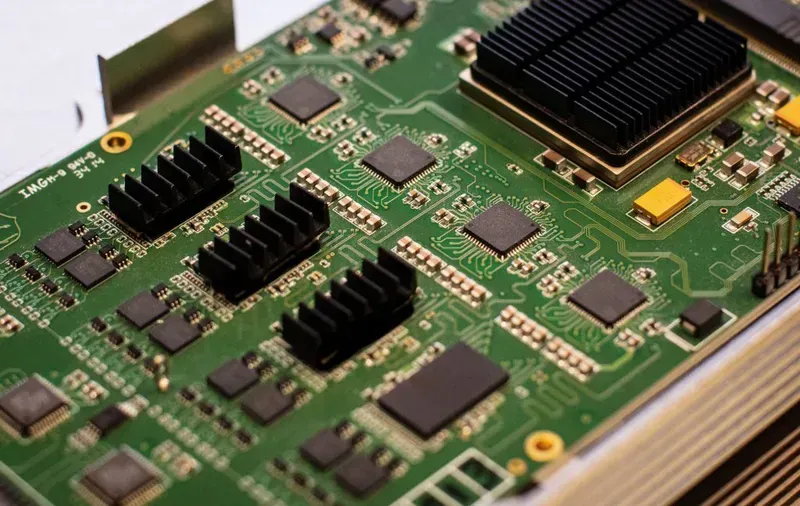
Ultrasonic Imaging Processing Board
At the heart of every advanced ultrasonic imaging system, from critical medical diagnostics to precision industrial non-destructive testing, lies the ultrasonic imaging processing board. This sophisticated electronic backbone is pivotal for transforming raw ultrasonic signals into clear, actionable visual data. Its functions encompass the entire imaging chain: high-fidelity signal acquisition, complex digital signal processing (DSP) for noise reduction and enhancement, and ultimately, real-time image reconstruction. The relentless demand for superior image resolution, rapid data transfer, and minimal noise interference in both medical and industrial applications necessitates high-performance, robust, and exceptionally reliable processing board solutions that can withstand the rigors of continuous operation while delivering unparalleled accuracy.
Signal Acquisition and Digitization The board's primary role is to receive analog ultrasonic echoes from transducers, amplify them with precision, and convert them into digital data at extremely high sampling rates. This initial stage is critical as any distortion or noise introduced here will propagate throughout the entire imaging process, compromising image quality.
Digital Signal Processing (DSP) Once digitized, the raw data undergoes extensive DSP. This involves complex algorithms for beamforming, filtering, compression, and other enhancements to remove artifacts, improve signal-to-noise ratio, and focus the ultrasonic energy. Advanced DSP capabilities are essential for distinguishing subtle tissue variations or detecting minute defects in materials.
Image Reconstruction and Rendering Following processing, the board reconstructs the data into a visual image. This involves sophisticated algorithms to render 2D, 3D, or even 4D (real-time 3D) images, often requiring dedicated graphics processing units (GPUs) for rapid visualization. The speed and accuracy of this stage directly impact the user's ability to interpret the ultrasonic data effectively.
High-Speed Data Transfer Ultrasonic imaging generates massive volumes of data in real-time. The processing board must support high-bandwidth interfaces (e.g., PCIe, Gigabit Ethernet) to transfer this data quickly and efficiently to display units or storage, ensuring smooth, lag-free imaging performance.
Low Noise Operation Maintaining an ultra-low noise floor is paramount. Even minor electrical noise can obscure faint echoes, particularly in deep tissue imaging or detecting small flaws. The board's design must incorporate meticulous shielding, grounding, and power integrity strategies to minimize interference and preserve signal fidelity.
Reliability and Durability Especially in medical applications where lives depend on accurate diagnoses, the processing board must demonstrate exceptional reliability and long-term durability. This necessitates rigorous component selection, robust manufacturing processes, and comprehensive testing to ensure consistent performance under various operating conditions.
Challenges in Designing Ultrasonic Imaging Boards
Engineer with Ultrasonic Transducer
Designing and manufacturing high-performance ultrasonic imaging processing boards presents a multifaceted array of engineering challenges that demand deep expertise in high-frequency electronics. These boards are the backbone of precise diagnostic and industrial ultrasound systems, and their effective operation hinges on meticulous attention to detail in every design phase. Overcoming these hurdles is paramount to ensuring signal accuracy, image clarity, and the overall reliability of the final ultrasonic transducer board, directly impacting the success of a custom ultrasonic electronics solution. Zero One Solution Limited, with its extensive experience, understands these complexities intimately and offers robust solutions to mitigate them.
Challenge Area
Description & Impact
Solution Approach
High-Frequency Signal Management
Ultrasonic signals operate at high frequencies (MHz range), requiring precise impedance control and minimal signal loss. Improper handling leads to signal degradation, reduced resolution, and inaccurate imaging.
Advanced material selection (low Dk/Df), meticulous trace routing, impedance matching techniques, and sophisticated simulation tools.
Electromagnetic Interference (EMI) Minimization
High-speed digital and analog circuits can generate significant EMI, corrupting sensitive ultrasonic signals. This causes noise, artifacts, and unreliable performance in imaging systems.
Strategic component placement, effective grounding schemes, shielding, careful power plane design, and isolation of analog/digital sections.
Signal Integrity (SI) & Power Integrity (PI)
Maintaining clean signals and stable power delivery across complex multi-layer boards is critical. SI/PI issues manifest as reflections, crosstalk, voltage drops, and ground bounce, compromising data accuracy.
Stack-up optimization, controlled impedance traces, decoupling capacitors, robust power distribution networks (PDN), and comprehensive pre-layout simulations.
Complex Multi-Layer Designs
High component density and complex interconnections necessitate multi-layer PCBs, increasing design complexity and potential for errors. This impacts manufacturing yield and board reliability.
High-speed processing and power components generate heat, which can degrade performance, reduce component lifespan, and affect signal stability. Effective heat dissipation is crucial for long-term reliability.
Thermal vias, heat sinks, strategic component placement for airflow, thermal simulation, and material selection with good thermal conductivity.
Why is high-frequency signal management so critical for ultrasonic imaging boards? High-frequency signal management is critical because ultrasonic signals operate in the megahertz range. Any degradation or loss of these signals due to improper impedance control, reflections, or crosstalk directly impacts the quality of the ultrasound image. Precise control ensures that the weak echoes received by the transducer are accurately amplified and processed, which is fundamental for achieving high-resolution and artifact-free images essential for diagnostics and industrial inspection. Without meticulous high-frequency design, the system's ability to discern fine details or detect subtle anomalies is severely compromised, rendering the imaging data unreliable or unusable.
Successfully navigating these intricate challenges requires not only state-of-the-art design tools and processes but also an experienced engineering team. Zero One Solution Limited brings this precise blend of technological capability and seasoned expertise to every ultrasonic imaging board project, ensuring that our clients receive a robust, high-performance solution that meets the most demanding application requirements.
Zero One Solution Limited's Expertise in High-Frequency PCB Design
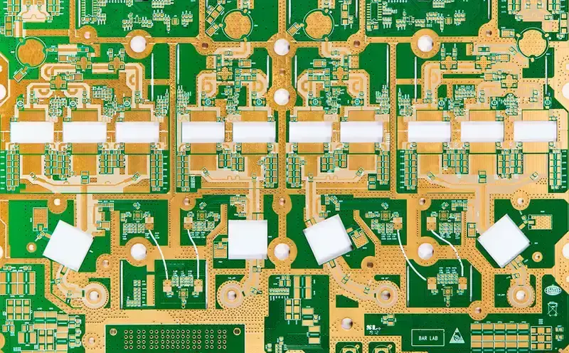
High-Frequency PCB Design
At Zero One Solution Limited, our deep expertise in high-frequency PCB design is foundational to delivering superior Ultrasonic Imaging Processing Board Solutions. The precision and integrity of signals are paramount in ultrasonic applications, demanding meticulous attention to design parameters such as impedance control, material dielectric properties, optimized stack-ups, and advanced routing strategies. Our proven track record in overcoming these complex challenges ensures that every board we produce meets the stringent performance requirements for high-resolution ultrasonic imaging, solidifying our position as a leader in custom ultrasonic electronics design and manufacturing.
Impedance Control Excellence Achieving precise impedance control is critical for high-frequency signal transmission in ultrasonic imaging boards. We employ advanced simulation tools and design methodologies to ensure consistent impedance across all signal paths, minimizing reflections and maximizing signal integrity. This rigorous approach is crucial for maintaining the fidelity of ultrasonic signals, which are often in the MHz range or higher, directly impacting image clarity and diagnostic accuracy. Our experience with various trace geometries and ground plane configurations allows for optimal impedance matching for diverse transducer requirements and data rates, from standard 50-ohm lines to custom differential pairs for sensitive analog front-ends.
Optimized Material Selection The choice of PCB substrate material significantly impacts high-frequency performance. We carefully select materials with low dielectric loss (Df) and stable dielectric constant (Dk) across the operating frequency range, such as Rogers, Isola, or specialized high-Tg FR-4 variants. This selection is critical in minimizing signal attenuation and distortion, ensuring that the subtle ultrasonic echoes are accurately captured and processed. Our material expertise extends to understanding thermal expansion characteristics and their influence on long-term reliability in demanding medical and industrial environments. We also consider the mechanical properties of materials to ensure robust board construction, especially for portable or harsh environment ultrasonic devices, which often experience vibration and shock.
Design Aspect
Zero One Solution Limited's Approach
Impact on Ultrasonic Imaging
Stack-Up Optimization
Multi-layer designs with optimized ground planes and power distribution networks, ensuring signal isolation and minimizing crosstalk.
Reduces noise and interference, leading to clearer, more precise ultrasonic images and reliable system operation across all channels and modes (e.g., B-mode, Doppler).
Advanced Routing Techniques
Differential pair routing with length matching, controlled impedance routing, and careful via transitions to maintain signal integrity and prevent signal degradation.
Preserves the integrity of high-speed data from ADCs and to FPGAs, essential for accurate image reconstruction and rapid processing of complex algorithms. This ensures that the time-of-flight measurements and amplitude variations are precisely captured for high-resolution imaging, enhancing the detection of minute anomalies or structural details.
What makes high-frequency PCB design challenging for ultrasonic imaging? High-frequency PCB design for ultrasonic imaging is challenging due to several factors: signal integrity issues at high frequencies (e.g., reflections, attenuation, crosstalk), the need for precise impedance control, careful material selection to minimize dielectric loss, managing thermal dissipation from high-speed processing components, and minimizing electromagnetic interference (EMI) that can corrupt sensitive analog signals. Zero One Solution Limited addresses these by employing advanced simulation tools, precise routing strategies, and optimal material choices to ensure signal fidelity and system reliability.
Zero One Solution Limited stands as a premier provider of comprehensive solutions for ultrasonic imaging processing boards, simplifying the entire product development lifecycle from concept to market. Our integrated 'one-stop' approach consolidates schematic design, layout, component sourcing, PCB manufacturing, assembly, and rigorous testing, ensuring a streamlined and efficient process for our clients. This holistic service model is meticulously tailored to address the intricate demands of both medical imaging PCB solutions and robust industrial ultrasound transducer boards, providing a unified platform for innovation and accelerated deployment.
Integrated Design & Layout Services Our expert engineers utilize advanced EDA tools to create precise schematic designs and optimized PCB layouts, focusing on high-frequency signal integrity, impedance control, and noise reduction essential for superior ultrasonic imaging. We handle complex multi-layer designs with meticulous attention to detail.
Global Component Sourcing & Management Leveraging our extensive global supply chain network, we efficiently source high-quality, authentic electronic components critical for ultrasonic imaging boards. Our strategic locations in Shenzhen and Dubai ensure competitive pricing and timely delivery, mitigating supply chain risks.
Precision PCB Manufacturing We employ state-of-the-art manufacturing processes to produce high-density interconnect (HDI) PCBs suitable for the demanding specifications of ultrasonic applications. Our capabilities include specialized material selection for high-frequency performance and stringent quality control at every stage.
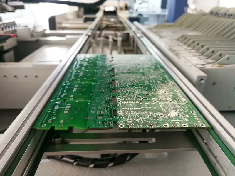
Advanced PCB Assembly (PCBA) Our assembly services encompass both Surface Mount Technology (SMT) and Through-Hole Technology (THT), with a focus on precision placement and soldering. We utilize automated optical inspection (AOI) and X-ray inspection to ensure flawless assembly, crucial for the reliability of ultrasonic imaging systems.
Rigorous Testing & Validation Every ultrasonic imaging board undergoes comprehensive functional testing, electrical parameter verification, and environmental stress screening. Our rigorous testing protocols ensure that each board meets performance specifications, industry standards, and regulatory requirements, guaranteeing reliability and safety.
Rapid Prototyping: Accelerating Your Time to Market
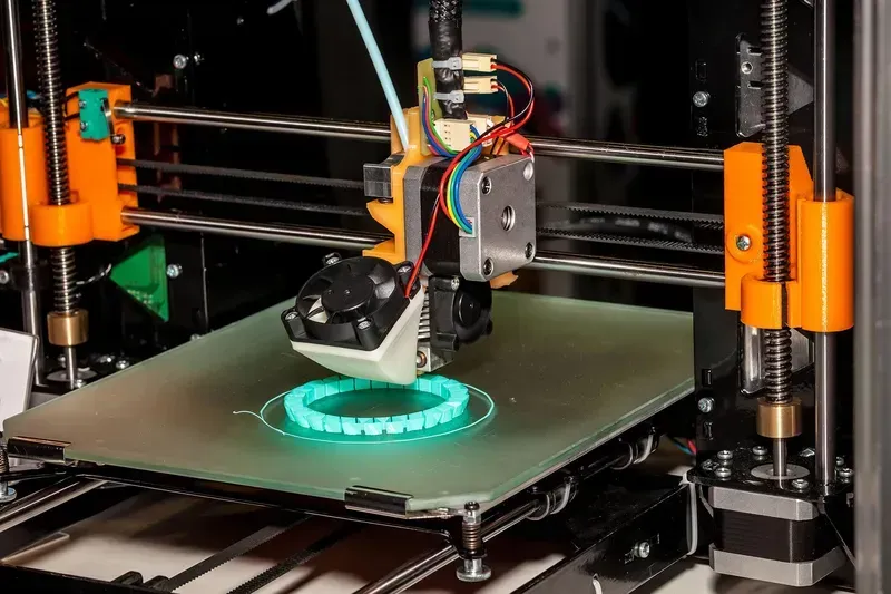
Rapid Prototyping Machine
Rapid prototyping is a cornerstone for innovation in the fast-paced world of ultrasonic imaging, allowing engineers and product developers to quickly transform concepts into tangible prototypes, test their functionality, and iterate designs with unprecedented speed. This accelerated development cycle is critical for gaining a competitive edge, validating designs swiftly, and ultimately reducing the time it takes to bring advanced ultrasonic imaging processing board solutions to market. For a reliable custom ultrasonic electronics partner like Zero One Solution Limited, mastery of rapid prototyping is not just an advantage; it's a necessity for empowering our clients to innovate faster and more efficiently.
Reduced Development Cycles Our rapid prototyping services drastically cut down the time from design to functional prototype. By streamlining the PCB fabrication and assembly process, we enable multiple design iterations in a fraction of the traditional timeframe. This agility is invaluable for complex ultrasonic imaging systems where iterative refinement is key to optimal performance and cost-effectiveness. Clients can test concepts, identify flaws, and implement improvements faster, leading to a more mature and robust product upon launch. Our rapid-response R&D prototype manufacturing significantly reduces project timelines, translating directly into faster market entry for our clients' innovative products.
Prototyping Benefit
Traditional Prototyping
Zero One Solution Rapid Prototyping
Turnaround Time (PCB Fab)
Weeks
Days
Iteration Speed
Slow, high cost per iteration
Fast, cost-effective iterations
Design Validation
Delayed
Accelerated
Market Entry
Extended
Significantly Faster
Beyond speed, rapid prototyping minimizes risks by allowing early detection of design flaws, ensuring that large-scale manufacturing proceeds with a thoroughly validated and optimized design. This significantly reduces the likelihood of costly rework and delays later in the product lifecycle. Zero One Solution Limited's commitment to rapid prototyping for ultrasonic imaging processing boards provides a distinct strategic advantage, fostering innovation and ensuring market readiness.
Quality Assurance and Reliability in Medical Applications
Medical Device Quality Testing
In the realm of medical imaging, particularly with ultrasonic systems, the integrity and reliability of the processing board are not merely a preference but a non-negotiable imperative. A robust ultrasonic imaging board solution directly impacts diagnostic accuracy and patient safety. Zero One Solution Limited understands that every component, every trace, and every solder joint on a medical imaging PCB solution must meet the highest standards of quality and performance to ensure faultless operation in critical applications.
Why is quality assurance critical for ultrasonic imaging processing boards? Quality assurance is paramount for ultrasonic imaging processing boards because they are the nerve center of medical diagnostic equipment. Any defect or inconsistency can lead to erroneous imaging data, misdiagnoses, or even system failure, directly jeopardizing patient care. Rigorous quality control ensures signal integrity, minimizes noise, and guarantees the precise functioning required for accurate medical assessments.
What industry standards do Zero One Solution Limited adhere to for medical imaging PCBs? Zero One Solution Limited strictly adheres to globally recognized industry standards relevant to medical device manufacturing and PCB production, including ISO 13485 (Medical Devices Quality Management Systems) and IPC Class 2 or 3 (for high-reliability electronics). These standards govern design, manufacturing, testing, and documentation, ensuring that every medical imaging PCB solution meets stringent regulatory and performance requirements for safety and efficacy.
How does Zero One Solution Limited ensure the reliability of its ultrasonic imaging board solutions? Our commitment to reliability is upheld through a multi-faceted approach. This includes meticulous material selection for high-frequency applications, advanced design techniques for signal integrity and thermal management, and a comprehensive suite of testing protocols. We employ functional testing, environmental stress screening, and in-circuit testing to identify and rectify any potential issues before delivery, guaranteeing a robust ultrasonic imaging board solution.
What specific testing procedures are implemented for medical imaging PCB solutions? Zero One Solution Limited implements rigorous testing procedures specifically tailored for medical imaging PCB solutions. These include Automated Optical Inspection (AOI) for solder joint quality, X-ray inspection for hidden defects, In-Circuit Test (ICT) for component functionality, and comprehensive functional testing that simulates real-world operating conditions to validate overall board performance, signal accuracy, and power integrity.
How does Zero One Solution Limited’s quality focus benefit clients in medical applications? Our unwavering focus on quality provides clients in medical applications with unparalleled peace of mind. By delivering exceptionally reliable and high-performance ultrasonic imaging board solutions, we help reduce design iterations, minimize failure rates in the field, accelerate regulatory approvals, and ultimately enable faster market entry for their innovative medical devices. This translates to enhanced product reputation and improved patient outcomes.
The advancement of ultrasonic imaging technology is directly tied to the sophistication of its underlying hardware. Zero One Solution Limited stands as your trusted partner in navigating the complexities of ultrasonic imaging processing board development. With our deep expertise, rapid prototyping capabilities, and commitment to quality, we transform your concepts into market-ready solutions. From initial design to final assembly, our one-stop service ensures efficiency and excellence. Don't let manufacturing complexities hinder your innovation. Connect with Zero One Solution Limited today to discuss how our ultrasonic imaging processing board solutions can elevate your next project and accelerate your path to success.