In the rapidly evolving landscape of medical technology, CT scanners stand as pillars of modern diagnostics, providing invaluable insights into the human body. At the heart of every high-performance CT scanner lies sophisticated signal processing, a critical function enabled by highly specialized Printed Circuit Boards (PCBs). As a veteran engineer at Zero One Solution Limited, a leader in rapid prototyping and one-stop PCB solutions since 2011, I understand the immense challenges and paramount importance of these components. This article delves into how Zero One Solution's expertise in CT Scanner Signal Processing PCB Solutions empowers medical device manufacturers to achieve unparalleled diagnostic clarity, accelerate product development, and bring life-saving innovations to market with unmatched efficiency. We will explore the intricate demands of these PCBs and how our tailored approach ensures superior performance and reliability.
The Critical Role of Signal Processing PCBs in CT Scanners
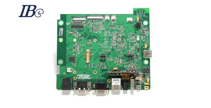
CT Scanner PCB Board
In the sophisticated world of medical imaging, the clarity and diagnostic accuracy of a CT scan hinge critically on the underlying signal processing capabilities. At the heart of this complex system lies the Printed Circuit Board (PCB), an often-understated component that functions as the nervous system of the CT scanner. These specialized PCBs are responsible for receiving, digitizing, and transmitting the minute electrical signals generated by X-ray detectors, translating them into the high-resolution images clinicians rely on. Their role extends beyond mere connectivity; they are the unsung heroes ensuring data integrity, minimizing noise, and facilitating the rapid data throughput essential for precise image reconstruction, directly impacting diagnostic reliability and patient safety.
Why are Signal Processing PCBs so crucial for CT scanner image quality? Signal Processing PCBs in CT scanners are fundamental to image quality because they are directly responsible for the accurate capture, conditioning, and conversion of analog signals from X-ray detectors into digital data. Any impedance mismatch, noise, or timing inaccuracies introduced by the PCB can lead to artifacts, blurring, or distortion in the final image, compromising diagnostic precision. High-speed, low-noise designs ensure the fidelity of these signals, which is paramount for reconstructing clear, detailed cross-sectional images of the human body. The precision of these PCBs ensures that minute variations in X-ray attenuation, indicative of different tissue types, are accurately translated into corresponding pixel values, thus enabling high-contrast resolution and subtle lesion detection crucial for early diagnosis and treatment planning. Without a meticulously designed signal processing PCB, the sophisticated algorithms for image reconstruction would be fed corrupted data, rendering even the most advanced CT scanner ineffective.
Challenges in Designing CT Scanner Signal Processing PCBs
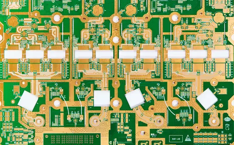
High-Frequency PCB Design
Designing signal processing PCBs for CT scanners presents a formidable array of engineering challenges that demand meticulous attention to detail and advanced expertise. The precision required for diagnostic imaging means that any deviation in signal integrity or processing can significantly impact image quality and diagnostic accuracy. These challenges extend from managing incredibly high-frequency signals and mitigating noise to ensuring data integrity across complex digital pathways and effectively managing thermal loads, all while rigorously adhering to stringent medical regulatory standards.
High-Frequency Signal Management CT scanners utilize rapid data acquisition, necessitating PCBs capable of handling high-frequency analog and digital signals without degradation. This involves careful impedance control, trace length matching, and precise routing to minimize reflections and ensure signal fidelity, which is critical for accurate data capture from the detector array.
Noise Minimization and EMI/EMC Compliance The subtle electrical signals from CT detectors are highly susceptible to noise. Designing for minimal electromagnetic interference (EMI) and ensuring electromagnetic compatibility (EMC) is paramount. This requires strategic grounding, shielding, filtering, and component placement to prevent internal and external noise sources from corrupting the raw data. Compliance with standards like IEC 60601-1-2 is non-negotiable.
Data Integrity and High-Speed Interfacing CT scanners generate massive volumes of data in real-time, requiring robust data integrity mechanisms. The integration of high-performance Analog-to-Digital Converters (ADCs) and Digital Signal Processors (DSPs) is central to this. Challenges include designing interfaces that can reliably transmit gigabits of data per second while maintaining signal quality and preventing data loss or corruption, often through sophisticated error correction schemes.
Thermal Management High-speed components like ADCs and DSPs generate significant heat. Effective thermal management, through strategic PCB layout, selection of thermal vias, and integration with cooling solutions, is essential to maintain optimal component performance and prevent reliability issues or premature failure, ensuring consistent operation over extended periods.
Regulatory Adherence (ISO 13485 & FDA) Beyond technical performance, CT scanner PCBs must strictly comply with global medical device regulations. ISO 13485 (Medical Devices - Quality Management Systems) and FDA guidelines (e.g., 21 CFR Part 820) dictate every stage of design, manufacturing, and documentation. This requires rigorous design controls, risk management, traceability, and validation processes to ensure patient safety and device efficacy.
Component Selection and Reliability Choosing medical-grade components with proven reliability and long-term availability is vital. This often involves sourcing specialized parts with extended temperature ranges, low noise characteristics, and certified lifespan, adding complexity to the supply chain and requiring thorough vetting of component manufacturers.
Zero One Solution's Expertise in High-Performance PCB Design
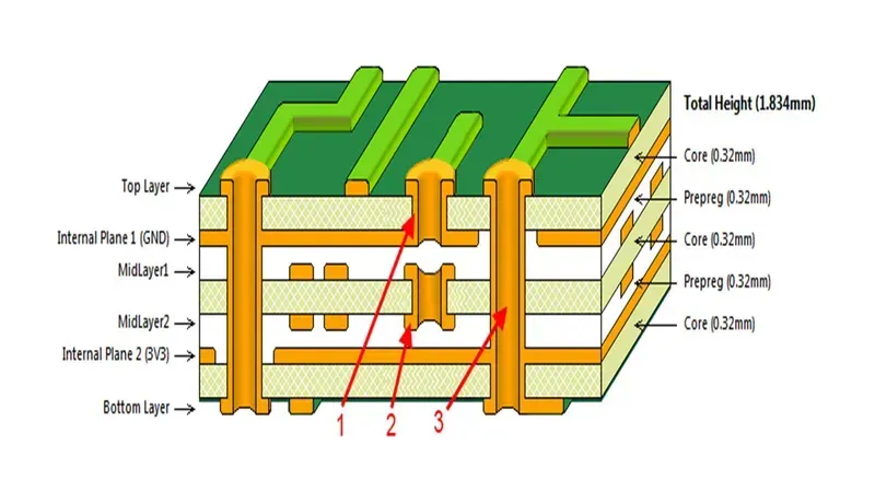
Multi-Layer PCB Design Engineer
At the core of a CT scanner's exceptional diagnostic capabilities lies a sophisticated signal processing Printed Circuit Board (PCB). These PCBs demand unparalleled precision and reliability due to the high-speed data acquisition and processing required for accurate image reconstruction. Zero One Solution Limited, with over a decade of experience as a premier PCB solution provider, brings a deep well of expertise in crafting high-performance, medical-grade PCBs that meet the stringent requirements of CT scanner signal processing, ensuring data integrity and operational stability.
Advanced Design Capabilities for High-Speed and Mixed-Signal PCBs Our proficiency extends to the intricate world of high-speed digital and mixed-signal PCB design. We meticulously manage critical parameters such as impedance control, ensuring signal integrity across high-frequency transmission lines. Our design methodologies also prioritize crosstalk reduction, minimizing interference between adjacent traces, which is crucial for the clear, artifact-free signals essential in CT imaging. Furthermore, we excel in power integrity analysis, delivering stable and clean power distribution networks that prevent voltage drops and noise, vital for sensitive analog-to-digital converters (ADCs) and digital signal processors (DSPs) within CT scanners.
Thermal Management Solutions for Sustained Performance The continuous operation of CT scanners generates significant heat, which can severely impact PCB performance and longevity. Zero One Solution employs advanced thermal management strategies during the design phase, including optimized component placement, efficient heat sink integration, and the selection of materials with superior thermal conductivity. This proactive approach ensures that our CT Scanner Signal Processing PCBs maintain optimal operating temperatures, preventing thermal throttling and guaranteeing reliable, long-term performance even under demanding operational loads.
Mastery of Complex Multi-Layer Designs and Advanced Materials The intricate nature of CT scanner signal processing often necessitates complex multi-layer PCB designs. Our engineers are highly skilled in navigating the complexities of designs with 16, 24, or even more layers, optimizing trace routing, power planes, and ground planes for maximum signal fidelity and minimal electromagnetic interference (EMI). We leverage advanced PCB materials, such as low-loss laminates (e.g., Rogers, Isola) and high-Tg materials, which offer superior dielectric properties and thermal stability, crucial for the high-frequency environments found in CT systems.
Commitment to Medical Device Standards and Compliance Understanding the critical nature of medical devices, our design and manufacturing processes are rigorously aligned with international medical standards. We adhere to ISO 13485 for medical device quality management systems and consider FDA guidelines throughout the development lifecycle. This commitment ensures that every CT Scanner Signal Processing PCB we produce is not only technically superior but also fully compliant with the stringent regulatory requirements of the medical industry, facilitating smoother product approvals for our clients.
Rapid Prototyping and Manufacturing for Medical Devices
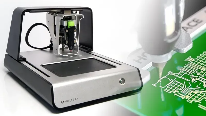
PCB Rapid Prototyping
In the fast-evolving landscape of medical technology, speed to market is paramount for CT scanner innovation. Zero One Solution Limited stands at the forefront of this demand, offering rapid prototyping and advanced manufacturing services that significantly accelerate the R&D cycle for medical device manufacturers. Our specialized capabilities enable swift iteration and validation of critical CT Scanner Signal Processing PCB designs, ensuring that groundbreaking diagnostic tools reach patients faster and more efficiently.
Accelerated R&D Cycle for Medical PCBs Zero One Solution’s rapid prototyping services are engineered to streamline the development timeline for CT scanner PCBs. We understand that each design iteration in medical device development is crucial. Our agile processes, combined with advanced simulation tools and expert engineering support, allow for quick fabrication of functional prototypes. This drastically reduces the time from concept to validation, empowering manufacturers to test, refine, and optimize their CT scanner signal processing PCBs with unprecedented speed. This efficiency not only saves valuable development time but also minimizes costly redesigns.
State-of-the-Art Manufacturing Facilities Our manufacturing facilities are equipped with cutting-edge technology specifically tailored for the demanding requirements of medical-grade PCBs. We maintain strict adherence to industry standards and regulations, ensuring that every CT Scanner Signal Processing PCB manufactured meets the highest levels of quality and reliability. Key features of our manufacturing capabilities include:
Advanced Material Handling Precise handling and processing of specialized substrates and laminates essential for high-frequency signal integrity in CT scanners.
Precision Fabrication Utilizing high-precision drilling, etching, and plating techniques for complex multi-layer PCB structures common in signal processing applications.
Clean Room Environment Maintaining controlled environments to prevent contamination, crucial for the longevity and performance of medical electronics.
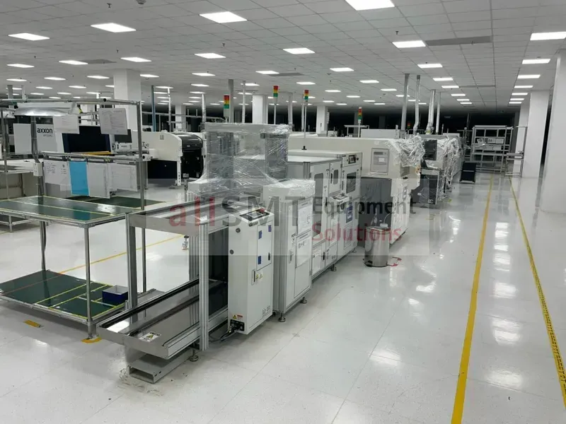
Automated Assembly Lines High-speed SMT (Surface Mount Technology) lines ensure accurate placement of miniature and complex components typical in CT scanner signal processing units.
Rigorous Quality Control and Testing Quality assurance is non-negotiable for medical devices. Our commitment to excellence is reinforced by stringent quality control processes integrated throughout the manufacturing lifecycle. For CT Scanner Signal Processing PCBs, we employ advanced inspection and testing methodologies to guarantee flawless performance and regulatory compliance. These include:
Automated Optical Inspection (AOI) Ensures precise component placement and solder joint integrity, identifying defects that are imperceptible to the human eye, vital for densely populated CT scanner PCBs.
X-ray Inspection (AXI) Provides non-destructive inspection of hidden solder joints (e.g., under BGA and QFN packages) and internal PCB layers, crucial for verifying the complex interconnections within signal processing boards.
In-Circuit Testing (ICT) Verifies the functionality of individual components and checks for manufacturing defects like short circuits or opens, ensuring electrical integrity of the entire circuit.
Functional Testing (FCT) Simulates the operational environment of the CT scanner, confirming that the signal processing PCB performs according to design specifications and meets all performance benchmarks.
Environmental Testing Includes thermal cycling and humidity testing to ensure the PCB's reliability and durability under various operating conditions within a CT scanner.
Comprehensive One-Stop Solution: From Design to Assembly
PCB Assembly Line
Zero One Solution Limited provides a comprehensive, one-stop service for CT Scanner Signal Processing PCB solutions, seamlessly integrating every phase from initial schematic design to final assembly and rigorous testing. This integrated approach is crucial for accelerating product development in medical imaging, ensuring that complex, high-performance PCBs meet the exacting standards of CT scanner technology while significantly reducing lead times and project complexities.
Integrated Design & Development Our process begins with collaborative schematic design, working closely with clients to translate their CT scanner signal processing requirements into robust electronic blueprints. This is followed by meticulous PCB layout, where our engineers optimize signal integrity, power distribution, and thermal performance, especially critical for the sensitive analog and high-speed digital circuits in CT scanners. Our expertise in multi-layer designs ensures optimal routing and minimized interference for high-fidelity signal acquisition and processing.
Precision Component Sourcing & Fabrication Leveraging our extensive global supply chain network, we ensure reliable and cost-effective sourcing of medical-grade components, including specialized ADCs, DSPs, and low-noise op-amps essential for CT scanner signal processing. Our fabrication processes adhere to the highest industry standards, utilizing advanced materials and manufacturing techniques to produce PCBs with exceptional reliability and consistency, compliant with ISO 13485.
Advanced Assembly (PCBA) & Rigorous Testing The assembly phase employs state-of-the-art SMT and through-hole technologies to ensure precise component placement and robust solder joints. Crucially, our comprehensive testing protocols, including Automated Optical Inspection (AOI), X-ray Inspection (AXI), and in-circuit testing (ICT), are specifically tailored for the stringent performance requirements of CT scanner PCBs. Functional testing simulates real-world operating conditions to validate signal processing accuracy, noise performance, and overall system reliability, guaranteeing the highest quality medical device components.
Global Reach and Supply Chain Excellence
Zero One Solution Limited leverages its strategic global presence to ensure unparalleled supply chain excellence for critical CT Scanner Signal Processing PCB solutions, offering medical device manufacturers timely access to diverse component markets and robust logistical support worldwide. Our dual operational hubs in Shenzhen, China, and Dubai, UAE, are not merely physical locations but key enablers of a resilient, cost-effective, and agile global supply chain tailored to the demanding requirements of medical electronics.
Strategic Locations for Global Advantage Our headquarters in Shenzhen, China, positions us at the epicenter of global electronics manufacturing, granting immediate access to an extensive ecosystem of high-quality component suppliers and advanced fabrication facilities. This proximity to the supply chain's core allows for rapid prototyping and mass production with optimized lead times and cost efficiencies. The Dubai branch office serves as a crucial bridge, connecting us to the European, Middle Eastern, and African markets, facilitating expedited logistics, local support, and enhanced responsiveness for clients in these regions. This dual-hub strategy mitigates geopolitical risks and ensures continuous, unhindered access to essential resources for CT Scanner Signal Processing PCB manufacturing.
Enhanced Supply Chain Resilience In an era of increasing supply chain volatility, Zero One Solution's distributed network significantly enhances resilience. By diversifying sourcing channels and logistics routes across multiple geographies, we minimize exposure to single-point failures and disruptions. This proactive approach ensures a consistent and reliable flow of specialized components and raw materials required for complex CT Scanner Signal Processing PCBs, safeguarding against delays and maintaining project timelines for our medical device partners. Our robust inventory management and predictive analytics further bolster this resilience, anticipating and mitigating potential supply chain bottlenecks.
FAQs about CT Scanner Signal Processing PCB Solutions
Optimizing CT scanner signal processing PCBs is paramount for diagnostic accuracy and patient safety. This section addresses common inquiries about the design, manufacturing, and testing of these critical components, offering expert insights into the intricate requirements for high-performance medical electronics, including material selection, EMI/EMC compliance, and crucial lifecycle management considerations.
What are the primary challenges in designing a CT Scanner Signal Processing PCB? Designing CT scanner signal processing PCBs involves managing extremely high-frequency analog and digital signals, minimizing noise interference (EMI/EMC), ensuring thermal stability for sensitive components, and guaranteeing data integrity at high throughputs. Adherence to stringent medical regulatory standards (e.g., ISO 13485, FDA 21 CFR Part 820) is also a significant challenge, requiring robust design for reliability and longevity, as well as meticulous documentation and traceability throughout the entire product lifecycle.
What specific materials are crucial for CT Scanner Signal Processing PCBs? For CT scanner signal processing PCBs, specialized materials are crucial. High-Tg (glass transition temperature) laminates are used for thermal stability, low Dk (dielectric constant) and Df (dissipation factor) materials like high-performance FR-4, polyimide, or specialized ceramic-filled laminates are essential for maintaining signal integrity at high frequencies and minimizing signal loss. Copper foil with excellent conductivity and surface finishes like ENIG (Electroless Nickel Immersion Gold) or ENEPIG (Electroless Nickel Electroless Palladium Immersion Gold) ensure superior solderability and signal transmission while offering corrosion resistance.
How is EMI/EMC compliance ensured in CT Scanner Signal Processing PCBs? EMI/EMC compliance for CT scanner signal processing PCBs is achieved through a multi-faceted approach. This includes meticulous PCB layout techniques such as careful trace routing for impedance control, proper grounding schemes (e.g., solid ground planes), strategic component placement to minimize loop areas, and effective shielding. Additionally, filtering components (e.g., ferrite beads, common-mode chokes, bypass capacitors) are integrated, and signal integrity simulations are performed during the design phase. Rigorous testing in an anechoic chamber or EMC test facility verifies compliance with medical EMC standards like IEC 60601-1-2 before product release.
What testing protocols are applied to CT Scanner Signal Processing PCBs? Beyond standard electrical tests, CT scanner signal processing PCBs undergo comprehensive testing. This includes in-circuit testing (ICT), functional testing at operational frequencies and temperatures, signal integrity analysis (e.g., eye diagram analysis, jitter measurement), and specific performance validation for critical parameters like ADC/DAC accuracy, noise floor, and dynamic range. Environmental stress screening (ESS) such as thermal cycling and vibration testing ensures reliability under various conditions, while accelerated life testing (ALT) helps predict product longevity in the field. All testing is meticulously documented to meet regulatory requirements.
In conclusion, the journey from concept to a high-performing CT scanner hinges significantly on the precision and reliability of its signal processing PCBs. Zero One Solution Limited stands as your premier partner in navigating these complexities, offering a comprehensive, one-stop solution from cutting-edge design to rapid manufacturing and assembly. Our strategic global presence, coupled with a relentless commitment to rapid-response R&D prototyping, ensures that your innovations not only meet but exceed the stringent demands of medical imaging. Partner with Zero One Solution to accelerate your product development cycles, reduce time to market, and ultimately, contribute to the advancement of medical diagnostics worldwide. Contact us today to discuss how our CT Scanner Signal Processing PCB Solutions can transform your next medical imaging project.