In our increasingly interconnected world, copper clad boards are the unsung heroes behind countless electronic devices. From the smartphones in our pockets to the complex systems powering industries, these foundational components play a crucial role. This article delves into the nature of copper clad boards, examining their diverse types, applications, and offering a guide to selecting the right board for your next project. We'll explore not only how they're used in electronics but also what it takes to bring them from a raw board to a functional circuit. Get ready to demystify the world of copper clad boards and uncover how they enable so much of modern technology.
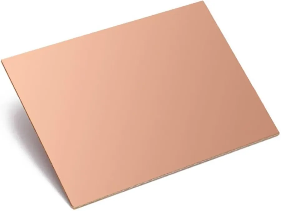
A copper clad board, at its core, is a composite material engineered for the fabrication of printed circuit boards (PCBs). It consists of a base substrate, typically a non-conductive material like fiberglass or a composite, onto which a thin layer of copper foil is bonded. This copper layer is the conductive medium that allows for the creation of electrical pathways. The base substrate provides mechanical support and electrical insulation.
The performance of a copper clad board is determined by the properties of both the base substrate and the copper foil. The substrate's mechanical strength and thermal resistance impact the board's reliability. The copper foil’s thickness, purity and adhesion affect its electrical conductivity. The manufacturing process ensures that the copper layer is firmly adhered to the substrate, which is critical for reliable performance. Let's look at these in more detail.
| Layer | Material | Role | Key Properties |
|---|---|---|---|
| Base Substrate | FR-4 (Fiberglass Epoxy), CEM-1, Phenolic | Provides mechanical support and electrical insulation | Mechanical strength, thermal resistance, electrical insulation |
| Copper Foil | Copper | Provides a conductive pathway for electrical signals | Conductivity, thickness, adhesion |
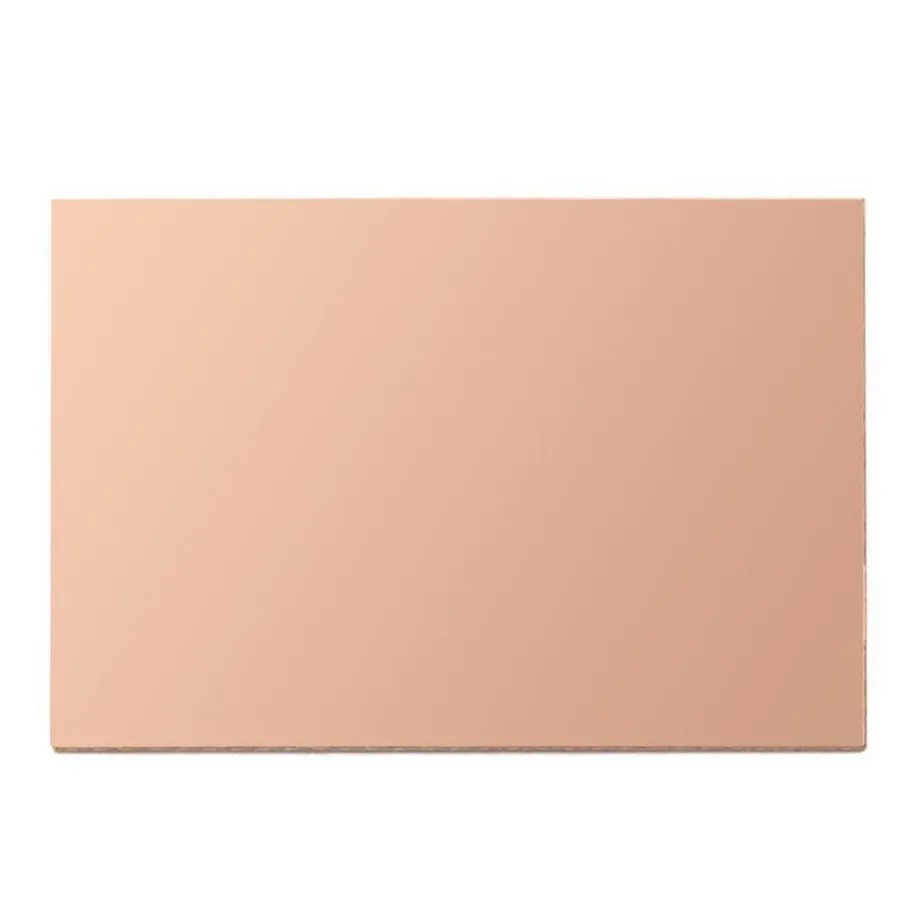
Copper clad boards are fundamental to electronics manufacturing, serving as the base for printed circuit boards (PCBs). They are available in several configurations, each tailored for different applications based on complexity, cost, and performance requirements. The primary types are single-sided, double-sided, and multi-layered boards, each offering distinct advantages and disadvantages.
| Type | Description | Complexity | Cost | Typical Applications |
|---|---|---|---|---|
| Single-Sided | Copper layer on one side of the substrate. | Lowest | Lowest | Simple electronics, educational projects, basic prototyping |
| Double-Sided | Copper layers on both sides of the substrate. | Medium | Medium | Intermediate-complexity electronics, common consumer devices, moderate power applications |
| Multi-Layered | Multiple copper layers separated by insulating material. | Highest | Highest | High-density electronics, advanced computing, telecommunications, aerospace |
The selection of copper clad board type should be driven by the specific project requirements. Single-sided boards are ideal for basic applications where complexity and performance demands are low. As complexity and performance demands increase, double-sided and multi-layered boards are more appropriate. The increased costs associated with the double-sided and multi-layered options are offset by the capabilities and densities they enable.
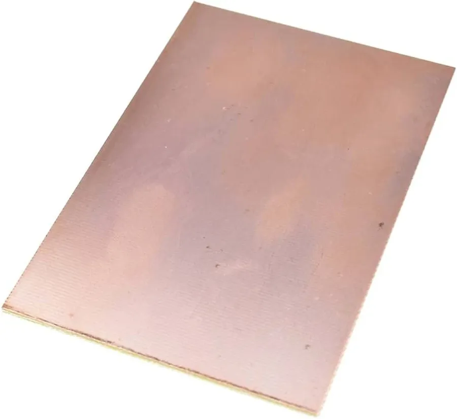
The performance and suitability of a copper clad board are heavily influenced by the base materials used. Common substrates include FR-4, CEM-1, and phenolic, each offering a unique combination of properties concerning fire resistance, mechanical strength, and cost. Selecting the appropriate base material is crucial to achieving the desired performance for a given application.
| Material | Fire Resistance | Mechanical Strength | Cost | Typical Applications |
|---|---|---|---|---|
| FR-4 | Good (Self-extinguishing) | High | Moderate | General-purpose PCBs, consumer electronics, industrial control systems |
| CEM-1 | Moderate | Moderate | Lower | Single-sided PCBs, cost-sensitive applications, less demanding environments |
| Phenolic | Low (Flammable) | Low | Low | Simple, low-cost applications, such as educational kits, non-critical electronics |
FR-4 (Flame Retardant type 4) is the most commonly used substrate for PCBs. It is a composite material made of woven fiberglass cloth with an epoxy resin binder. FR-4 offers a good balance of electrical properties, mechanical strength, and fire resistance, making it suitable for a wide variety of applications. While slightly more expensive than CEM-1 and phenolic, its versatility and reliability make it the preferred choice for many projects. CEM-1 (Composite Epoxy Material 1) is a composite material consisting of a paper substrate with a fiberglass layer and an epoxy resin binder. It offers a cost-effective alternative to FR-4 for less demanding applications. Phenolic is the least expensive substrate material, primarily composed of paper bonded with a phenolic resin. It exhibits lower mechanical strength and is not flame retardant, limiting its use to simple, non-critical electronics where cost is the primary consideration.
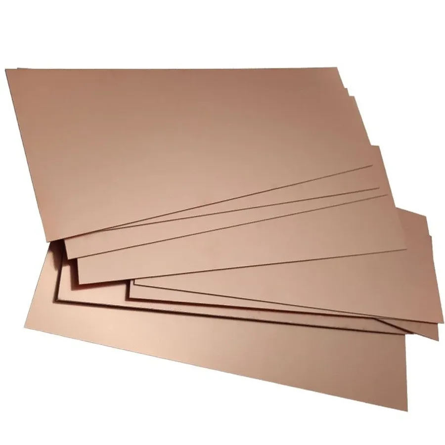
Copper thickness, typically measured in ounces per square foot (oz/ft²), is a critical parameter in copper clad boards that directly influences their electrical performance. This measurement refers to the weight of copper spread over a one square foot area and dictates the board's ability to handle electrical current without overheating or experiencing signal degradation. The appropriate copper thickness ensures the reliable operation of electronic circuits.
| Copper Thickness (oz/ft²) | Approximate Thickness (µm) | Typical Applications | Current Carrying Capacity |
|---|---|---|---|
| 0.5 oz | 17.5 µm | Low-power signal circuits, simple hobby projects | Lower |
| 1 oz | 35 µm | General-purpose electronics, most common thickness | Moderate |
| 2 oz | 70 µm | Higher current applications, power electronics | Higher |
| 3 oz or more | 105 µm+ | High-power applications, demanding thermal management | Very High |
The current-carrying capacity of a copper trace increases with thickness, but also with trace width. The thicker the copper, the more current it can handle without excessive heat build-up, making it a critical design factor in ensuring longevity of the board. Selecting the proper thickness is crucial, balancing performance requirements, cost, and manufacturing considerations.
For low-power applications, such as signal processing or simple digital circuits, a standard 1 oz/ft² copper layer is generally sufficient and cost-effective. In contrast, high-power applications, such as motor controllers or power supplies, require thicker copper layers (2 oz/ft² or more) to manage the higher current levels, prevent overheating, and ensure that the electrical performance is not compromised.
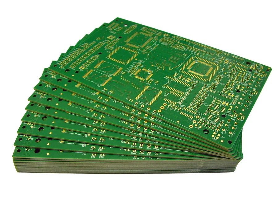
Copper clad boards serve as the foundational building blocks for a vast array of electronic devices and systems, owing to their versatility and essential role in circuit construction. They facilitate the creation of printed circuit boards (PCBs), which are integral to nearly all modern electronics, from simple consumer gadgets to sophisticated industrial machinery.
The widespread adoption of copper clad boards stems from their fundamental role in creating functional electronic systems and facilitating innovation across countless industries. Their adaptability allows them to be utilized in a plethora of applications, meeting the diverse needs of both individual creators and large-scale manufacturers.
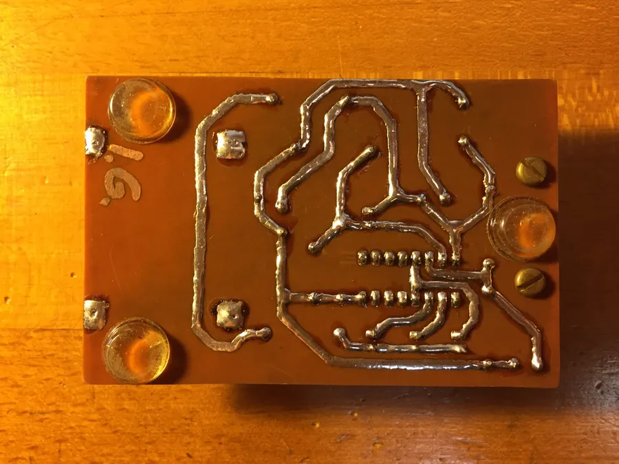
Etching is a critical process in creating custom Printed Circuit Boards (PCBs) from copper clad boards. It involves selectively removing copper from the board, leaving behind the desired circuit traces. This process requires careful planning and execution to achieve accurate and reliable results.
The etching process typically involves several key steps:
Safety Precautions are critical when working with etchants, as these chemicals are corrosive and can cause burns or irritation. Always wear appropriate personal protective equipment, including gloves, eye protection, and a lab coat or apron. Ensure proper ventilation is used when etching, as fumes can be harmful. Dispose of used etchant solutions appropriately, according to local regulations.
| Etchant Type | Description | Advantages | Disadvantages | Typical Usage |
|---|---|---|---|---|
| Ferric Chloride (FeCl3) | A common etchant, usually supplied as a solid and mixed with water. Turns copper into soluble copper chloride | Relatively inexpensive, easy to use, works at room temperature, long shelf life | Stains easily, etches relatively slowly, solution is opaque making it difficult to see the etching process, highly corrosive, produces corrosive waste. | Home etching, educational purposes, small scale projects. |
| Ammonium Persulfate ((NH4)2S2O8) | An alternative etchant which is also mixed with water. Copper is dissolved as a copper sulfate salt. | Clear solution enables real time visual observation, Fast etching rate, less prone to staining. | More expensive than ferric chloride, produces a less stable solution with limited shelf life, can be temperature dependent. | High precision or rapid prototyping, applications where visibility is important, professional production. |
This section addresses common questions regarding copper clad boards, providing clear and concise answers to aid understanding and decision-making.
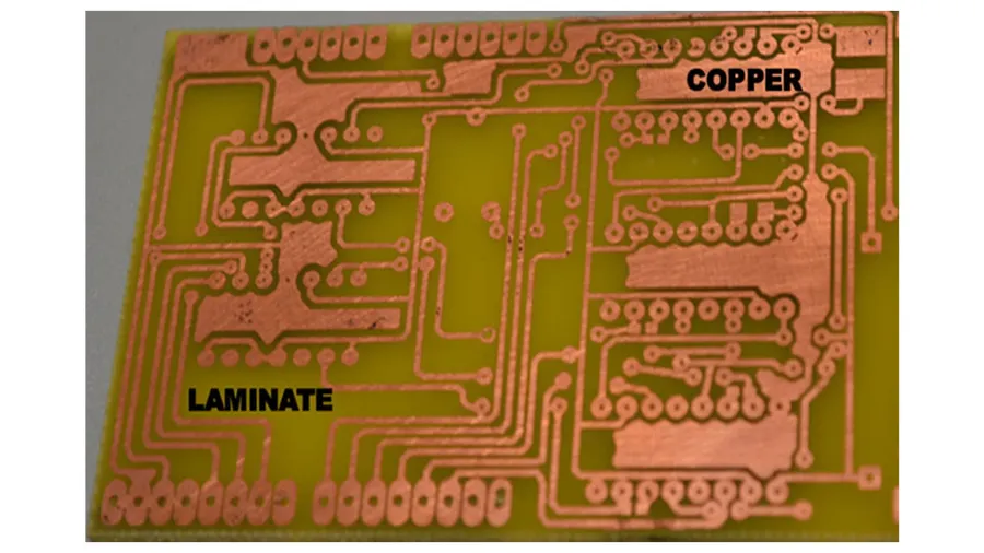
Choosing the correct copper clad board is crucial for the success of any electronics project, whether it's a simple prototype or a complex commercial product. The selection process involves balancing several critical factors: size, material, copper thickness, and budget. A systematic approach to these considerations ensures optimal performance and cost-effectiveness.
By systematically considering these factors, you can make informed decisions that align with your project requirements, leading to more reliable and successful outcomes in your electronics projects.
Copper clad boards are indispensable components in the world of electronics, from simple DIY projects to advanced industrial applications. Understanding their types, materials, and proper handling techniques is crucial for anyone involved in electronics design and development. We've covered a wide range of topics, from the fundamentals of the copper clad board structure to practical etching methods and selection criteria. The ongoing advancements in material science and manufacturing promise further innovations in this field. Armed with this knowledge, you're better equipped to navigate the world of copper clad boards and bring your electronic ideas to life.

