In our increasingly wireless world, RF PCBs are the unsung heroes enabling seamless communication. From your smartphone to sophisticated radar systems, these specialized circuit boards handle high-frequency signals critical for modern technology. This guide delves into the essential aspects of RF PCB design, offering practical insights and expert advice to navigate this complex yet crucial field. We'll bridge the gap between theory and practice, ensuring you understand the ‘why’ behind every design choice.
Understanding the Fundamentals of RF PCBs
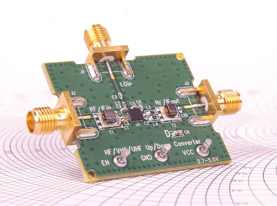
RF PCB Board
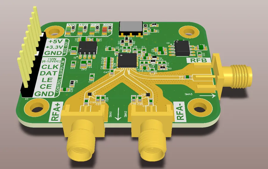
RF PCBs, engineered to manage radio frequency signals typically exceeding 100 MHz, diverge significantly from standard PCBs due to the stringent demands of high-frequency operation. These demands include precise impedance control, maintaining signal integrity, and minimizing signal losses, which are crucial for reliable performance. This section delves into these distinctions and their profound effects on PCB design.
Key Differences Between RF PCBs and Standard PCBs RF PCBs require a heightened focus on impedance matching, signal integrity, and minimizing losses due to the high frequencies they handle, unlike standard PCBs where such parameters are less critical.
Frequency Range of RF PCBs RF PCBs operate at frequencies typically above 100 MHz, extending into the GHz range. This high-frequency operation necessitates specialized design considerations not found in lower-frequency PCB applications.
Impact of RF Design on Performance The specific design considerations in RF PCBs, such as material selection and layout, directly impact performance characteristics like signal transmission quality, noise levels, and overall system efficiency.
Feature
Standard PCB
RF PCB
Frequency Range
Typically below 100 MHz
Typically above 100 MHz, extending into GHz
Impedance Control
Less critical
Highly critical for signal integrity
Material Selection
Primarily FR-4
Specialized materials like PTFE or Rogers often required
Signal Integrity
Less stringent requirements
Stringent requirements to minimize losses and reflections
Design Considerations
Simpler layout practices
Specific routing techniques, ground plane designs, and shielding methods
Material Selection for RF PCBs
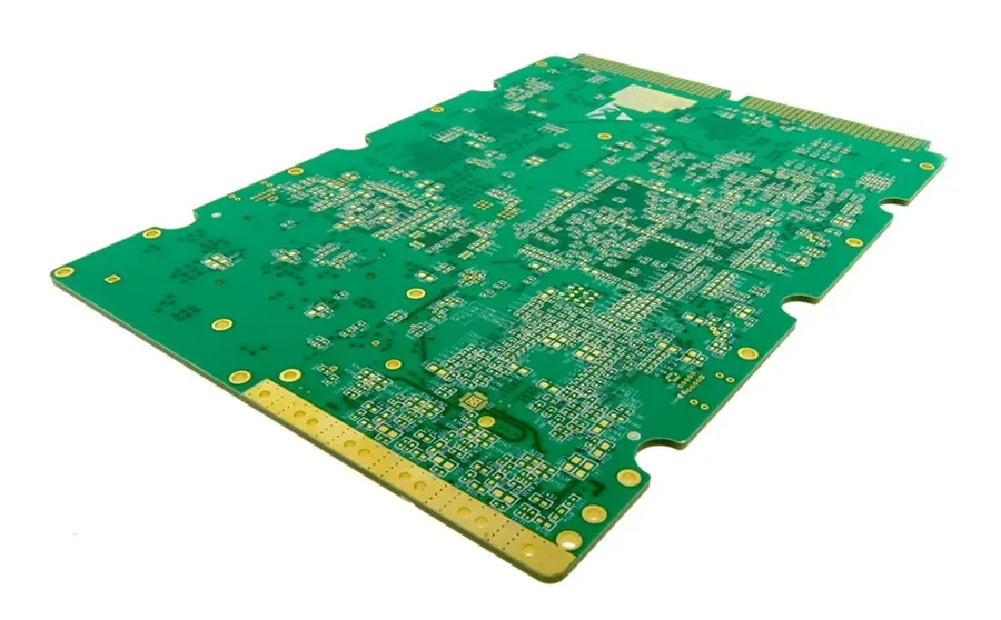
RF PCB Materials
The selection of materials for RF PCBs is paramount, as it directly influences high-frequency performance. Key material properties, including dielectric constant (εr), dissipation factor (tan δ), and thermal conductivity, dictate signal losses, impedance characteristics, and overall reliability. This section delves into the most common materials used and how their properties impact RF PCB design.
Material
Dielectric Constant (εr)
Dissipation Factor (tan δ)
Typical Applications
Advantages
Disadvantages
FR-4
4.3 - 4.8
0.02 - 0.03
Low-frequency RF, general purpose
Cost-effective, widely available
High loss at high frequencies, unstable εr
PTFE (Teflon)
2.1 - 2.6
0.0002 - 0.0005
High-frequency RF, microwave
Very low loss, stable εr
High cost, difficult to process
Rogers (Various)
2.2 - 10.2
0.0009 - 0.002
High-frequency RF, radar, aerospace
Low loss, stable εr, good thermal properties
Higher cost than FR-4
Dielectric Constant (εr) The dielectric constant of the PCB material determines the speed at which signals propagate. Lower dielectric constants typically lead to faster signal speeds and reduced losses. For high-frequency applications, materials with stable and low dielectric constants, such as PTFE and Rogers materials, are preferred. Variations in dielectric constant can cause impedance mismatch issues.
Dissipation Factor (tan δ) The dissipation factor (also known as the loss tangent) measures signal loss within the dielectric material. Lower values result in less signal attenuation. At higher frequencies, the dissipation factor becomes more significant, so selecting a low-loss material is crucial for high-performance RF designs. For example, PTFE exhibits much lower dissipation than FR-4.
Thermal Properties Thermal conductivity and the coefficient of thermal expansion are key considerations. RF circuits generate heat that can affect performance. Materials with good thermal conductivity help dissipate heat, improving reliability. The coefficient of thermal expansion should match that of the components to avoid stress during temperature fluctuations. Rogers materials often exhibit superior thermal performance compared to FR-4 and even PTFE.
Material Selection Trade-offs Choosing the correct material involves weighing performance against cost and manufacturability. FR-4 is cost-effective but performs poorly at high frequencies, making it unsuitable for most RF applications above a few GHz. High-performance materials like PTFE and Rogers offer superior performance but at a higher cost and may require specialized processing. Thus, careful consideration is essential, often involving balancing performance needs against budget and manufacturing capabilities. The selection should be carefully made based on the frequency band, power levels, and the operational environment the RF PCB will be used in.
Key Considerations in RF PCB Design
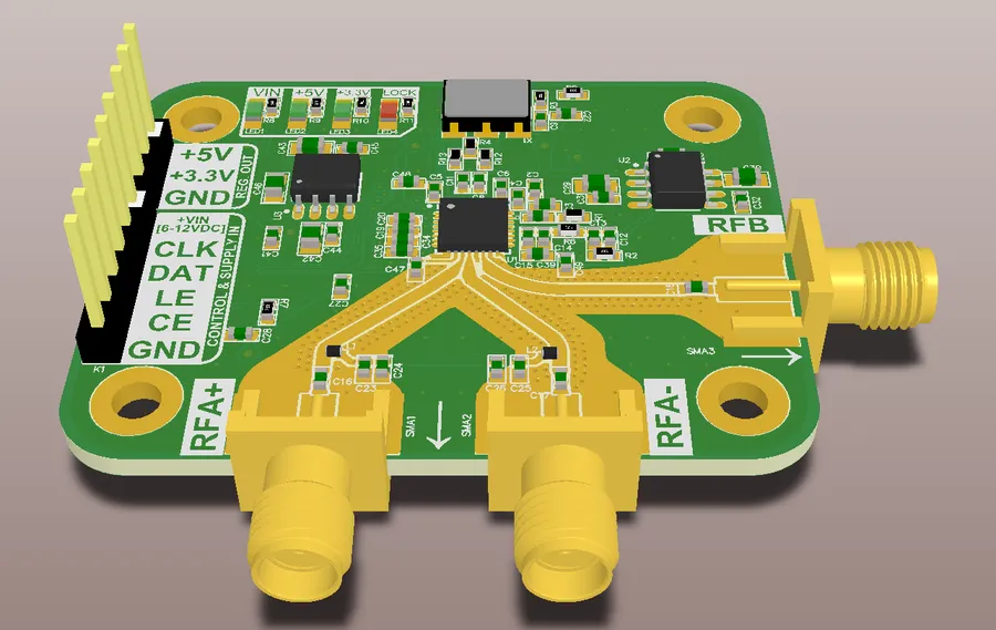
RF PCB Layout
Designing RF PCBs demands meticulous attention to detail, as these circuits operate at high frequencies where even minor imperfections can significantly impact performance. Key design considerations include impedance matching, trace routing, and the strategic use of ground planes, all of which are critical for maintaining signal integrity, minimizing signal reflections, and reducing noise in high-frequency applications.
Impedance Matching Ensuring that the impedance of the transmission lines matches the source and load impedances is crucial to minimize signal reflections and maximize power transfer. This requires careful calculation of trace widths and spacing to achieve the desired characteristic impedance, typically 50 ohms for most RF applications.
Trace Routing The path and geometry of signal traces directly affect signal integrity. Avoid sharp bends which can cause reflections. Keep trace lengths as short as possible and maintain consistent trace width to minimize impedance variations. Use controlled impedance routing techniques to minimize signal degradation.
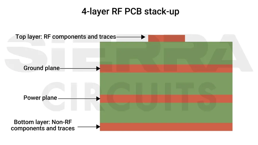
Ground Plane Design A solid, uninterrupted ground plane provides a stable reference potential and aids in shielding. Use a multi-layer PCB design where possible, dedicating at least one layer as a ground plane. Connecting all ground points to this plane with minimal vias ensures good signal return paths and reduces noise.
Via Management Vias, the plated holes that connect different layers of a PCB, can introduce impedance discontinuities and signal losses. Use as few vias as possible and optimize their size and placement. For high-frequency signals, consider using blind or buried vias to minimize their impact.
Component Placement The placement of RF components is paramount in reducing parasitic effects and maintaining the desired signal paths. Place components close to each other to minimize trace lengths and keep sensitive components away from noise sources. Prioritize component placement based on the critical signal paths.
Design Consideration
Impact on RF Performance
Mitigation Strategies
Impedance Mismatch
Signal reflections, power loss, standing waves
Use impedance matching techniques, controlled impedance transmission lines, careful calculation of trace geometry.
Poor Trace Routing
Signal distortion, increased losses, crosstalk
Minimize trace length, avoid sharp bends, use proper spacing, utilize differential pairs where required.
Dedicate a full layer to a solid ground plane, use multiple vias for connection, consider multi-layer boards.
Improper Via Usage
Impedance discontinuities, signal loss
Minimize via usage, optimize via placement, use blind or buried vias for critical signals.
Poor Component Placement
Increased parasitic effects, degraded signal paths
Place components close to each other, prioritize components on critical signal paths, keep sensitive components away from noise sources.
Impedance Control: Ensuring Signal Integrity
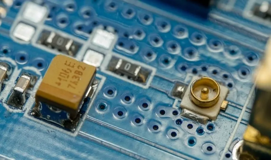
Impedance Controlled PCB
In Radio Frequency (RF) printed circuit board (PCB) design, impedance control is paramount for maintaining signal integrity and preventing signal reflections, thereby minimizing power loss and ensuring optimal performance. This involves carefully managing the characteristic impedance of transmission lines within the PCB to match the source and load impedances, thereby achieving maximum power transfer and minimal signal distortion.
The core concept revolves around designing transmission lines – the conductive paths on the PCB – to have a specific impedance value, typically 50 ohms for most RF applications. This is achieved through meticulous calculation and control of the trace geometry (width, height, and separation from the ground plane), as well as the dielectric properties of the PCB material. A mismatch in impedance will lead to signal reflections back to the source, reducing power efficiency, creating standing waves, and potentially damaging components. Different trace structures are employed to achieve controlled impedance, including microstrip and stripline, each with distinct characteristics and applications. Accurate impedance control therefore underpins the successful function of any RF PCB.
The characteristic impedance (Z0) of a transmission line is determined by its physical dimensions and the dielectric constant of the surrounding material. Common transmission line structures used in RF PCBs include microstrip and stripline. Microstrip lines are traces on the surface of the PCB with a ground plane on the layer below, while striplines are traces sandwiched between two ground planes. The formulas for calculating Z0 for microstrip and stripline are different, and rely on the parameters described in the table above. Achieving precise impedance requires careful planning, accurate manufacturing, and testing. Tools such as impedance calculators and simulators assist in the process. Accurate impedance control prevents signal degradation and maximizes RF performance.
Trace Design and Routing Techniques
RF PCB Trace Routing
Effective trace design and routing are paramount in RF PCB design to minimize signal loss and interference, ensuring optimal performance. This section will cover essential techniques, including avoiding sharp bends, controlling trace lengths, ensuring proper spacing, and utilizing differential pairs to maintain signal integrity in high-frequency applications.
Avoiding Sharp Bends Sharp bends in traces can cause impedance discontinuities, leading to signal reflections and losses. Instead, use smooth, curved traces with radii at least three times the trace width to ensure consistent impedance.
Controlled Lengths Matching trace lengths is critical, especially for differential pairs or parallel lines carrying the same signal. Variations in trace length can cause phase differences, degrading signal quality. Employ techniques like serpentine routing to equalize lengths.
Proper Spacing Between Traces Maintain adequate spacing between traces to minimize crosstalk and electromagnetic interference (EMI). Spacing should typically be 2 to 3 times the trace width. In high-density designs, use impedance-controlled spacing, usually with a 50 or 75 ohm target.
Differential Pairs Differential pairs, consisting of two closely routed traces, are effective for reducing noise and enhancing signal integrity. Ensure consistent spacing, length matching, and use of vias for both traces to maintain balanced signal propagation.
Via Considerations Use vias strategically, especially in high-frequency circuits where vias can introduce parasitic inductance and capacitance. Use a minimum number of vias, and make sure they are impedance-controlled, when used in signal traces.
Technique
Description
Benefit
Curved Traces
Use smooth curves instead of sharp bends.
Minimizes impedance discontinuities, reduces signal reflection.
Length Matching
Match the length of signal traces for parallel signals and differential pairs.
Reduces phase differences, maintains signal quality.
Trace Spacing
Maintain proper spacing between traces, typically 2-3 times the trace width.
Reduces crosstalk and EMI, improves signal integrity.
Differential Pairs
Route signal as closely matched pairs
Reduces noise and enhances signal integrity, balanced signal propagation
Ground Planes and Shielding
RF PCB Ground Plane
Effective ground plane design and strategic shielding are paramount in RF PCB design to minimize noise and ensure signal integrity. A well-implemented ground plane provides a stable reference for RF signals, while shielding techniques prevent unwanted interference between different circuit sections. Proper grounding and shielding significantly enhance the overall performance and reliability of RF circuits.
Continuous Ground Plane A continuous, unbroken ground plane provides the lowest impedance path for return currents, minimizing noise and signal reflections. Any discontinuities or splits in the ground plane can compromise signal integrity. Ideally, the ground plane should span the entire board area.
Ground Plane Layer Placement The placement of the ground plane layer within the PCB stack-up is critical. Typically, it is placed adjacent to signal layers to provide a close return path for signal currents. Having a solid ground plane directly underneath signal traces minimizes loop area, reducing inductance and emissions.
Via Stitching Via stitching involves using multiple vias to connect the ground plane layer at different points. This reduces impedance and inductance of the ground plane, and helps to maintain uniform ground potential throughout the PCB.
Shielding Techniques Shielding involves enclosing sensitive RF circuits within conductive enclosures (either metal cans or conductive material integrated into the PCB). These shields prevent electromagnetic interference (EMI) from external sources and prevent emissions from interfering with other parts of the PCB. The shield should be electrically connected to the ground plane to be effective.
Component Placement Component placement should also be considered for effective shielding. Placing sensitive components closer to the center of the board and surrounded by grounding helps mitigate external interference. Partitioning the board into functional areas can also aid in managing interference by localizing areas that are more susceptible to noise.
Grounding Different Circuit Sections Different sections of the RF PCB can have dedicated ground areas that connect to a main ground plane via low impedance connection. This helps to isolate digital and analog sections within an RF system, preventing high-frequency noise to influence sensitive RF circuits.
Grounding Technique
Description
Application
Advantages
Disadvantages
Continuous Ground Plane
Unbroken conductive layer on one or more PCB layers
General RF applications
Low impedance, minimal noise
May require larger board size
Via Stitching
Multiple vias connect the ground plane at different points
High-speed and RF applications
Reduces impedance, improves signal return
Increases manufacturing complexity
Shielding
Enclosing circuit within conductive material
Sensitive RF sections
Prevents EMI, reduces crosstalk
Increases design complexity and cost
Partitioned Grounding
Dedicated ground areas for different circuit sections
Mixed-signal RF systems
Isolates noise sources, improves stability
Requires careful planning of board layout
Thermal Management in RF PCBs
Effective thermal management in RF PCBs is crucial due to the heat generated by high-frequency circuits, which can significantly affect performance and reliability. Managing this heat through proper design techniques ensures the longevity and stable operation of the PCB.
Heat Sinks Heat sinks are essential components designed to dissipate heat away from the heat-generating components. They are typically made from materials with high thermal conductivity, such as aluminum or copper, and are attached to the PCB or directly to the hot components. The increased surface area of the heat sink facilitates heat transfer to the surrounding environment.
Thermal Vias Thermal vias are conductive holes that connect different layers of the PCB, allowing heat to transfer vertically through the board. These vias are strategically placed under or around heat-generating components to create a path for heat to flow to lower-temperature areas or heat sinks on the other side of the board. Copper-filled vias are often used due to copper's high thermal conductivity.
Component Placement Strategic component placement is crucial for thermal management. Placing high-power components close to the edges of the PCB allows heat to be dissipated more easily. Avoid grouping heat-generating components together in the center, as this can create hot spots. Proper spacing also enhances airflow and heat dissipation.
PCB Material Selection The choice of PCB material affects the heat dissipation. Materials with higher thermal conductivity help distribute heat more evenly across the board. The thermal conductivity of the dielectric material significantly affects the PCB temperature, with materials like metal-core PCBs providing better heat spreading capabilities compared to FR-4.
Airflow Management Ensuring adequate airflow around the PCB, especially in enclosed environments, aids in convective heat transfer. This can be achieved through strategic placement of air vents or cooling fans. The design of the enclosure can either impede or improve thermal performance.
Thermal Management Technique
Description
Advantages
Disadvantages
Heat Sinks
Physical devices attached to components to dissipate heat.
Increases PCB size and cost, requires proper mounting
Thermal Vias
Conductive vias to transfer heat vertically through the PCB.
Effective in multi-layer PCBs, can be implemented in design
May require specific design rules, can add manufacturing costs
Component Placement
Strategic placement of components to distribute heat.
Low-cost, simple to implement, highly effective.
Can complicate layout, requires careful planning
PCB Material Selection
Choosing materials with higher thermal conductivity
Improved heat spreading and dissipation
More costly materials, potentially more difficult to process
Airflow Management
Creating air channels for convective cooling
Cost effective method of thermal management.
Can require specific mechanical design, potentially large designs
RF PCB Assembly Frequently Asked Questions
The assembly of RF PCBs requires meticulous attention to detail due to the sensitive nature of high-frequency circuits. Proper techniques and considerations are crucial for ensuring optimal performance and reliability. Below are some frequently asked questions addressing critical aspects of RF PCB assembly.
What are the key considerations for component placement on an RF PCB? Component placement on an RF PCB is critical for minimizing signal interference and ensuring impedance matching. Key considerations include: keeping high-frequency components close to minimize trace lengths, avoiding 90-degree angles in traces, strategically placing decoupling capacitors, and ensuring proper ground connections to prevent noise and signal degradation. Components that handle high currents or generate heat should also be placed where they can be adequately cooled, avoiding sensitive RF components.
Which soldering techniques are recommended for RF PCB assembly? Reflow soldering is generally preferred for RF PCB assembly due to its precision and uniformity, which are critical for maintaining the integrity of high-frequency circuits. It's essential to use a controlled reflow profile to prevent thermal damage to components. For certain applications, manual soldering techniques may be necessary, especially for rework, but they should be performed with great care using low-temperature solders to avoid thermal stress. Careful control of solder paste application and flux is vital to maintain optimal connection quality and minimize void formation.
How does material selection impact the assembly of RF PCBs? Material selection significantly impacts RF PCB assembly, as different materials have varied thermal properties, dielectric constants, and mechanical strength. These characteristics affect the soldering process and the final operational reliability of the PCB. For instance, materials with high thermal conductivity may require more careful reflow profiles, and materials with low dielectric loss are chosen to maintain signal integrity during the assembly process. Proper material selection is crucial not only for performance but also for the robustness of the assembly.
How do you handle sensitive RF components during assembly? Sensitive RF components require careful handling during the assembly process to prevent damage from electrostatic discharge (ESD), physical stress, or contamination. ESD precautions, including the use of grounded workstations and wrist straps, are essential. Components should be stored in anti-static packaging and carefully placed using vacuum pick-up tools or similar methods to prevent physical damage. Moreover, components with fine leads should be aligned accurately during placement to ensure proper solder joint quality. Avoid any unnecessary touching of terminals.
What are the best practices for minimizing solder voids in RF PCB assembly? Minimizing solder voids is vital for the reliable performance of RF PCBs. Best practices include using high-quality solder paste with the correct viscosity, optimizing the reflow profile, and ensuring proper land pattern design on the PCB. Using nitrogen reflow, vacuum-assisted soldering, and preheating the PCB before the reflow can also significantly reduce voiding. The solder paste application process must also be controlled and inspected thoroughly to achieve optimal solder joint integrity. Minimizing solder voids is particularly important in RF circuits where high reliability is a must.
Are there special considerations for cleaning RF PCBs after assembly? Cleaning RF PCBs after assembly is necessary to remove flux residue and other contaminants that can degrade performance, especially at high frequencies. It's essential to use appropriate cleaning agents and methods that won't damage the PCB material or components. Ultrasonic cleaning with deionized water or specialized cleaning solvents may be required, followed by a thorough drying process to prevent corrosion. Residue from some cleaning chemicals or tap water can have ionic contaminants that are detrimental to RF performance.
How do I ensure proper thermal management during component assembly? Proper thermal management during assembly ensures the longevity and efficient operation of RF PCBs by preventing overheating of critical components. This is achieved through several methods. Using thermal vias to transfer heat from the components to a ground plane is essential. Heat-generating components should be placed near heat sinks. The PCB materials should have the capability of conducting heat away from hot spots. Finally, care must be taken to prevent excessive heating of components during the soldering process. This involves careful temperature control during reflow or manual soldering, as well as the judicious use of heat sinks to keep components within their operating ranges.
Testing and Troubleshooting RF PCBs
Rigorous testing and systematic troubleshooting are indispensable for ensuring that RF PCBs meet specified performance criteria. This section delves into essential testing methodologies, diagnostic techniques, and tools necessary for identifying and resolving issues in RF PCB design, encompassing impedance verification, signal integrity analysis, and noise characterization. Effectively addressing these areas ensures a robust and reliable final product.
Impedance Testing Utilizes a Time-Domain Reflectometer (TDR) to verify the characteristic impedance of transmission lines on the PCB. This test detects impedance discontinuities that can cause signal reflections and power loss. TDR measurements are crucial for validating impedance matching achieved during design.
Signal Integrity Analysis Evaluates the quality of signal transmission on the RF PCB. Measurements include signal rise and fall times, overshoot, undershoot, ringing, and eye diagrams. This analysis is critical for ensuring that the signal quality is within acceptable limits for proper operation. Specialized software tools are often used to simulate and analyze signal integrity.
Noise Measurements Quantifies the noise floor and spurious signals present in the RF PCB. Noise figure measurements and spectrum analysis are used to characterize the noise performance. This is important to determine the sensitivity and dynamic range of the circuit, using spectrum analyzers to detect unwanted signals and noise levels.
S-parameter Measurements Employs a Vector Network Analyzer (VNA) to measure scattering parameters (S-parameters), which describe the behavior of the RF circuit in terms of reflection and transmission. S-parameter measurements are used to verify impedance matching, gain, and isolation. This includes S11 (reflection coefficient), S21 (transmission coefficient), and others that help assess circuit performance.
Functional Testing Verifies whether the RF PCB operates as intended under different operating conditions. This includes testing the board with its intended signals, frequency ranges, and power levels. The functional testing is a combination of the tests above done in real application scenario to check if the PCB meet real product design requirements.
Common Troubleshooting Techniques Systematic approach to problem-solving, using signal tracing, visual inspection, and component substitution to identify faults. Start from the most simple possible point and check for common causes, such as poor solder joints, incorrect component values, and short circuits.
Signal Tracing Using an oscilloscope or signal tracer, follow the signal path through the circuit to find the point where the signal is lost or corrupted. Signal tracing is critical for diagnosing intermittent signal behavior.
Visual Inspection Careful inspection of the PCB for visible defects such as solder bridges, cracks, damaged components, or incorrect parts. Visual inspection often provides a rapid and direct path to the source of failures.
Component Substitution Replacing suspected faulty components with known good components to isolate the source of the problem. This technique helps to pinpoint components that may be damaged or outside specification.
Temperature Mapping Using thermal cameras or temperature sensors to identify hot spots on the PCB which may indicate faulty components or short circuits. Temperature mapping helps to identify issues that may not be obvious through visual inspection.
Mastering RF PCB design requires a deep understanding of high-frequency principles and careful attention to detail. From selecting appropriate materials to implementing robust signal integrity practices, every aspect is crucial for optimal performance. RF PCBs are the backbone of many advanced technologies, and with a solid understanding of the design considerations and assembly best practices detailed in this guide, you're well-equipped to tackle even the most complex RF design challenges, pushing the boundaries of what's possible with this essential technology.