Understanding HDI PCB Costs: A Comprehensive Guide
2025.01.14
In the fast-paced world of electronics, High-Density Interconnect (HDI) PCBs are pivotal for smaller, more powerful devices. But, the question of 'HDI PCB cost' often looms large. From smartphones to medical devices, these boards enable complex functionalities in compact spaces. This article dives deep into the factors affecting HDI PCB costs, empowering you to make informed decisions and optimize your budget without compromising quality. We'll demystify the pricing variations and explore strategies for cost-effective manufacturing.
What is an HDI PCB?
HDI PCB
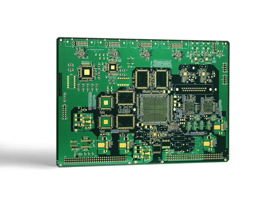
High-Density Interconnect (HDI) PCBs represent a significant advancement in printed circuit board technology, characterized by their higher wiring density per unit area compared to traditional PCBs. This increased density is achieved through the incorporation of microvias, fine lines, and high layer counts, allowing for more complex circuitry and greater functionality within smaller form factors. The design and manufacturing processes of HDI PCBs are more intricate, which impacts their cost.
Key characteristics of HDI PCBs include:
Microvias These are very small vias (typically less than 150μm in diameter) that connect different layers of the PCB, allowing for higher density routing.
Fine Lines and Spaces HDI PCBs feature narrower traces and smaller gaps between traces, further increasing component density.
High Layer Count HDI PCBs can have a large number of layers, enabling complex designs and advanced functionality.
Key Factors Influencing HDI PCB Cost
HDI PCB Layer Stack-up
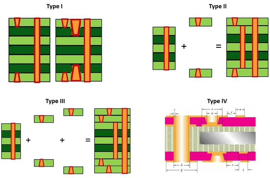
The cost of High-Density Interconnect (HDI) PCBs is determined by a multitude of factors, each contributing to the overall manufacturing expense. Understanding these drivers is crucial for effective cost management and design optimization. These factors encompass material selection, structural complexity, feature dimensions, and finishing processes, each of which will be detailed further in this section.
Factor
Description
Impact on Cost
Material Choices
Type of substrate material (e.g., FR-4, high-Tg epoxy, polyimide) and copper foil thickness.
Higher performance materials and thicker copper increase cost.
Layer Count
Number of conductive layers in the PCB.
More layers mean more processing steps and increased material consumption, leading to higher costs.
Feature Size
The width and spacing of traces and spaces, and the size of pads.
Finer features (smaller trace widths and gaps) require more precise manufacturing techniques, driving costs up.
Via Types
Types of vias used, including microvias, blind vias, and buried vias.
Microvias and other advanced vias add complexity and cost to the manufacturing process.
Surface Finish
The type of finish applied to the PCB's pads (e.g., HASL, ENIG, Immersion Silver).
Some finishes, like ENIG, are more expensive due to material costs and more complex plating processes.
Design Complexity
Overall complexity of the circuit design and layout.
More complex designs require additional manufacturing time and precision, therefore increasing costs.
Each of these elements can dramatically alter the price of an HDI PCB. The cost drivers, including the materials used, number of layers, the fineness of features, the choice of vias, the surface finish, and the design's intricacy, all play a vital role in determining the final price. For instance, employing high-performance materials such as polyimide, which offer better heat resistance and electrical properties than standard FR-4, substantially increases the cost. Similarly, the inclusion of microvias, which are critical for dense interconnects, adds to the complexity and therefore cost of manufacturing. A detailed understanding of these factors allows for strategic decision-making during design, helping to optimize costs without sacrificing performance.
HDI PCB Cost: A Volume-Based Perspective
PCB Mass Production
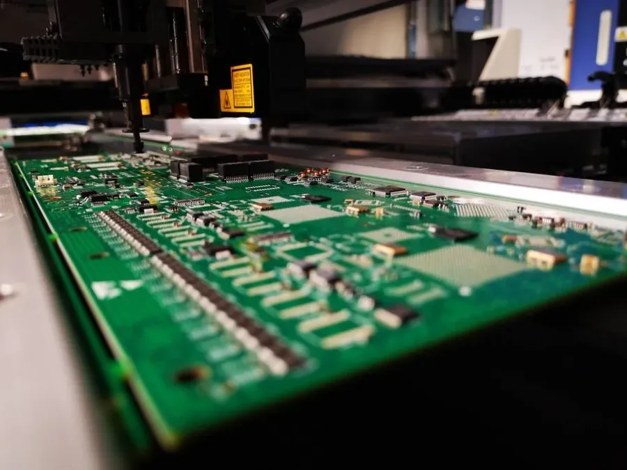
The cost of High-Density Interconnect (HDI) PCBs is significantly influenced by production volume. The unit cost decreases substantially as the quantity increases, shifting from higher per-unit expenses for prototypes to much lower costs in mass production runs. This is a fundamental aspect of manufacturing economics, where fixed costs are spread across a larger number of units.
Production Volume
Approximate Cost per Board
Manufacturing Process
Lead Time
Prototypes (1-10 boards)
$500 - $2000+
Manual assembly, focus on customization and design verification
2-4 weeks
Small Batches (10-100 boards)
$100 - $500
Semi-automated assembly, balancing cost and flexibility.
1-3 weeks
Medium Production (100 - 1000 boards)
$50 - $100
Automated assembly, optimization for moderate-volume
2-4 weeks
Mass Production (1000+ boards)
$10 - $50
Fully automated, high throughput
4-8 weeks
Cost-Saving Strategies for HDI PCB Manufacturing
Laser Drilling Microvias
Optimizing the manufacturing cost of HDI PCBs requires a strategic approach that balances performance with economic feasibility. Implementing cost-saving measures during the design and fabrication phases can significantly reduce overall expenses without sacrificing the essential functionalities of the board. These strategies involve careful planning and understanding of the manufacturing processes.
Optimize Layer Stack-Up Carefully planning the layer stack-up can minimize material usage and the number of fabrication steps. Aim for the fewest number of layers possible while still meeting the design requirements. Balancing the number of signal and power planes based on design needs can help reduce material usage and cost.
Standardize Design Features Using standard component footprints and design rules reduces the need for customized tooling and processes. This also allows for easier manufacturability, leading to faster production times and fewer errors, reducing the overall cost of PCB production.
Reduce Drilling Time Minimizing the number of vias, particularly microvias, can substantially reduce drilling time and cost. Blind and buried vias, while necessary in complex designs, should be used judiciously due to their increased manufacturing complexity. Explore alternative routing strategies that minimize the need for vias.
Select Cost-Effective Surface Finishes Choosing a surface finish that meets the application requirements but is not unnecessarily expensive. For example, ENIG (Electroless Nickel Immersion Gold) is a high-performing finish, but it is also more costly. Alternatives like HASL (Hot Air Solder Leveling) or OSP (Organic Solderability Preservative) may be sufficient for less demanding applications. Always balance performance with cost.
Panelization Optimization Efficient panelization can maximize the number of boards per manufacturing panel and thus reduce the per-unit cost. Work closely with your manufacturer to optimize panelization schemes, factoring in depanelization methods to avoid any material wastage.
Consider Material Choices While high-performance materials like high-Tg FR4 might be needed for specific applications, for most applications, standard FR4 materials will suffice and will be more cost-effective. Consider the trade-off between performance and cost when selecting core and prepreg materials.
Design for Manufacturability (DFM) Analysis Performing a DFM check early in the design process can identify potential manufacturing issues that could lead to higher costs during production. This includes addressing issues related to component placement, trace widths, and minimum spacing between features. By addressing DFM issues early on, cost overruns can be avoided and manufacturing yields will be improved.
HDI PCB vs. Standard PCB: A Cost Comparison
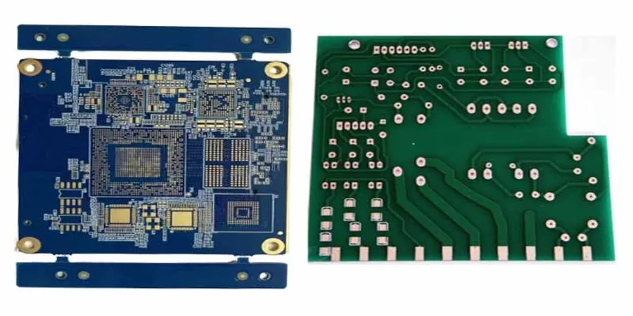
Standard vs HDI PCB Comparison
While High-Density Interconnect (HDI) PCBs offer superior performance and miniaturization capabilities, they generally come at a higher cost compared to standard PCBs. The choice between the two often hinges on the specific application requirements and budgetary constraints. This section provides a comparative analysis, highlighting when each PCB type is the more economically sound or technically suitable option.
Feature
Standard PCB
HDI PCB
Cost
Lower
Higher
Layer Count
Typically 1-16 layers
Often more than 8 layers, with sequential lamination
Feature Size
Larger traces and spaces
Finer traces and spaces, microvias
Via Technology
Through-hole vias
Microvias, blind vias, buried vias
Density
Lower component density
Higher component density
Performance
Suitable for basic applications
Superior performance in high-speed and complex designs
Application
Consumer electronics, low-frequency applications
Smartphones, wearables, medical devices, high-speed communication
Manufacturing Complexity
Simpler manufacturing process
More complex manufacturing process, multi-layer sequential lamination
Turnaround time
Shorter manufacturing time
Longer manufacturing time
Typical Cost Per Board
0.5-5 USD
3-30 USD
As demonstrated in the table, standard PCBs offer cost-effectiveness for basic designs with low density and performance requirements. However, when design complexity, miniaturization, and high performance are crucial, the higher cost of HDI PCBs becomes justifiable. Selecting the correct technology will align design needs with appropriate production costs.
How to Get an Accurate HDI PCB Quote
Obtaining an accurate quote for HDI PCBs requires a thorough understanding of the factors that influence cost and the ability to communicate these details clearly to manufacturers. Inaccurate or incomplete information can lead to misquotes, which can result in unexpected costs and delays.
To ensure you receive an accurate HDI PCB quote, focus on providing comprehensive specifications that allow manufacturers to precisely assess the complexity and resources needed for your project.
Detailed Gerber Files Provide complete and accurate Gerber files (RS-274X or equivalent). These files are the blueprint for your PCB and should include all layers, drill files, and solder mask details. Ensure that all necessary information is present and clearly labeled.
Layer Stack-up Details Clearly specify the layer stack-up, including the material types (e.g., FR-4, polyimide), copper weights, and the sequence of layers. Accurate layer information is crucial for costing and manufacturing processes.
Material Specifications Specify the desired base material (e.g., FR-4, Rogers), its thickness, and any special material requirements such as high TG, lead-free compliance, or halogen-free. Material choices directly impact cost and performance.
Via Type and Size Provide precise information on the number, size and type of vias used, including microvias, blind vias, and buried vias. Specify whether vias will be filled or capped, and the required plating thickness for the vias. Each via type has a significant impact on fabrication costs and is a crucial detail to include in your quote request.
Feature Size and Density Detail the minimum trace width, trace spacing, and via sizes. HDI PCBs are characterized by fine features; providing accurate information on these dimensions is necessary for accurate costing and manufacturability assessment.
Surface Finish Specify the required surface finish (e.g., ENIG, HASL, Immersion Tin/Silver/Gold). Different surface finishes have varying costs and properties, affecting both the budget and the board's longevity and solderability.
Quantity Indicate the precise production quantity required. Per-board costs are highly dependent on order volume; providing this number upfront helps in getting the most accurate cost estimate. Be clear about whether the quote is for prototyping, small-batch, or mass production.
Panelization Details If panelization is needed, clearly specify the panel size, the number of boards per panel, and the breakaway or routing method. Incorrect panelization will increase cost and may lead to manufacturing problems.
Special requirements Include any specific needs or compliance standards that must be followed, such as impedance control, specific testing protocols, or certifications requirements.
Pitfalls to Avoid When Requesting Quotes: When requesting quotes, avoid the following pitfalls to ensure accurate estimates:
Using incomplete or unclear documentation. Ensure that the information you provide is comprehensive, clearly labeled, and free of contradictions. Incomplete information leads to misquotes and delays.
Not specifying production quantity. Failure to specify your desired quantity can result in inaccurate price estimates. The unit cost will vary substantially between prototype and mass production volumes.
Failing to mention special requirements. If your boards require special materials, treatments, or adherence to specific standards, be sure to include these in the initial quote request. Omission of special requirement will result in an inflated final price.
HDI PCB Cost Calculators and Online Tools
Online HDI PCB cost calculators are readily available tools designed to provide initial cost estimates for PCB fabrication. While these tools offer a convenient starting point, it's crucial to understand their limitations and use them judiciously. They can provide a general idea of pricing based on basic parameters but should not replace a detailed quote from a manufacturer, especially for complex HDI PCBs.
These calculators typically allow you to input basic design parameters such as PCB dimensions, number of layers, material type, and quantity. Some advanced tools may also consider via types and surface finishes. However, these online tools often make simplifying assumptions about the manufacturing process, which can lead to inaccuracies, particularly for HDI PCBs that involve complex processes and specialized materials. Therefore, their output should be considered an approximation rather than a definitive quote.
To effectively utilize these tools for initial estimates, focus on the following: start by inputting the most accurate design parameters available, use several calculators to compare results, and verify outputs with manufacturer quotes. Remember to factor in additional costs such as testing, assembly, and tooling, which these calculators may not account for. These tools are best used for preliminary budgeting and comparison between different design choices, rather than for precise costing.
Advantages of Online HDI PCB Cost Calculators Quick initial cost estimates, allowing for rapid comparisons of different design options. They are readily accessible and require no specialized software installation, offering 24/7 availability.
Limitations of Online HDI PCB Cost Calculators They often lack the granularity needed for accurate cost assessment. Factors such as specific HDI features, advanced surface finishes, and complex layer stack-ups are hard to capture with these tools. These tools often use generalized formulas which may not accurately reflect the pricing structure of specific manufacturers or regional variations.
Best Practices for Using Online HDI PCB Cost Calculators Always start by accurately inputting the design parameters and compare the results from multiple sources for consistency. Use the results to refine the design and for initial budget planning. Treat the outputs as rough estimates, and always follow up with a formal quote from a manufacturer, especially for complex HDI PCB projects.
Frequently Asked Questions about HDI PCB Costs
Understanding the costs associated with HDI PCBs can be complex. This section addresses common queries to provide clarity and practical guidance. We aim to provide concise and insightful answers.
How much does an HDI PCB cost? The cost of an HDI PCB is highly variable, depending on complexity, layer count, material selection, and production volume. It's not a fixed price per board; prototypes could be several hundred dollars each, while mass production can reduce this dramatically. A general range can be from a few dollars for simple high-volume boards to hundreds for complex low-volume boards.
How much does one HDI PCB prototype cost? Prototyping costs are significantly higher due to setup fees, engineering time, and the smaller volumes. The cost for a single prototype HDI PCB can range from a few hundred to over a thousand dollars. This is because manufacturers need to prepare specific tools and processes for a small run which are not amortized across larger volumes.
What are the typical cost drivers for HDI PCB manufacturing? Key cost factors include the choice of materials (high-Tg, halogen-free, etc.), the number of layers (more layers, more cost), the complexity of features (microvias, blind vias, fine lines), the surface finish (ENIG, HASL), and the complexity of the design itself. Each of these factors adds to the fabrication complexity and associated costs.
How does production volume impact HDI PCB cost? The cost per unit decreases dramatically with increasing volume. High volume production allows manufacturers to amortize their initial setup costs and achieve economies of scale. Therefore, while a few prototype boards might be costly, the price per board decreases significantly in mass production.
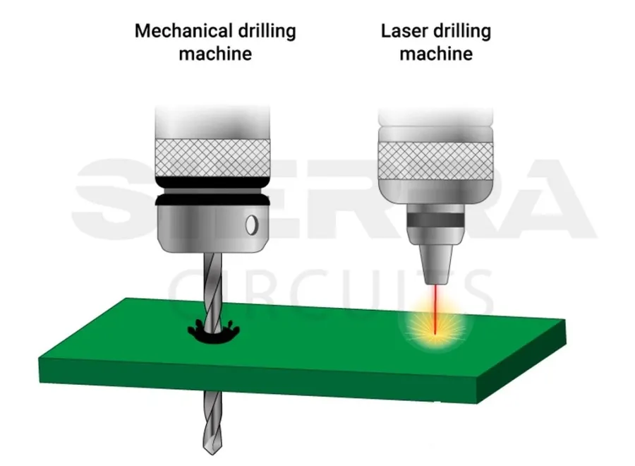
What is the impact of microvias on HDI PCB cost? Microvias are a significant cost driver because they require specialized drilling processes, laser technology, and increased fabrication time. The increased density and complexity they introduce elevates both the material and manufacturing costs.
How much does HDI PCB testing cost? The cost for testing an HDI PCB varies based on complexity. Simple electrical tests could be a small additional cost per board, but functional tests and thorough inspections can substantially increase this cost, especially for very intricate boards. Testing costs can range from a few dollars per board for basic tests to tens of dollars for comprehensive testing.
Can I reduce the cost of HDI PCBs? Yes, cost reduction strategies include optimizing the layer stack-up, simplifying the design, using standard component footprints, and carefully choosing surface finishes that meet your needs without being excessively expensive. Standardization reduces design complexity and manufacturing time, impacting the total cost.
Future Trends in HDI PCB Costs
Flexible HDI PCB
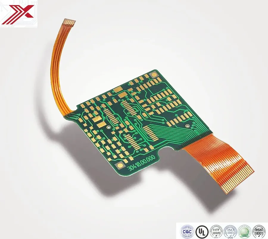
The landscape of HDI PCB manufacturing is constantly evolving, with emerging technologies and innovative manufacturing methods poised to significantly influence future costs. Advancements in materials, miniaturization techniques, and increased automation are key drivers that will reshape the pricing structure of high-density interconnect PCBs.
Specifically, the use of new materials with enhanced electrical and thermal properties will enable the production of smaller, more efficient HDI PCBs. As technology progresses, the demand for smaller form factors will drive innovation in miniaturization techniques, likely leading to lower per-unit costs and increased integration. Also, the automation of processes such as pick-and-place assembly, inspection, and testing is another area expected to considerably reduce manufacturing costs and enhance throughput in the coming years. The effect of these trends will be to lower the overall cost of HDI PCB technology over time, making it more accessible and feasible for a broader range of applications.
Advanced Materials The development of new substrate materials with superior electrical, thermal, and mechanical properties, leading to higher performance and potentially lower costs through streamlined processes and reduced material consumption.
Miniaturization Technologies Continued progress in miniaturization techniques, enabling denser designs with smaller feature sizes, which should translate to cost reduction as more functionality is packed into smaller areas.
Increased Automation Greater use of automation in manufacturing processes, including drilling, etching, and assembly, leading to faster production times, increased precision, and a reduction in labor costs, which in turn influences the final HDI PCB cost.
Additive Manufacturing Emerging technologies like 3D printing for PCB manufacturing may offer a different way to produce HDI PCBs, which potentially allows faster prototyping and customized production at lower costs.
Understanding the nuances of 'HDI PCB cost' is essential for making informed decisions in electronic product development. Factors ranging from design complexity and material selection to production volume significantly influence the final cost. By employing cost-saving strategies and choosing the right manufacturer, you can achieve a balance between budget and high-quality performance. As technology continues to advance, expect even more cost-effective HDI PCB solutions that will further drive innovation across industries. Remember to consider the total cost of ownership, including long-term reliability and performance, when making your choices about HDI PCB implementation.