The intricate dance of electronics often begins with a carefully crafted PCB (Printed Circuit Board) layout. But how much does this crucial step cost? Like a perfectly designed city plan guides its growth, the pcb layout price determines the trajectory of your electronics project. This article will delve into the real factors influencing PCB layout prices and arm you with strategies to optimize your budget without sacrificing quality. We'll explore the intricacies of cost estimation, from basic single-layer boards to complex multi-layer designs, drawing on real-world experiences to help you understand the financial side of your hardware endeavors. Through simple terms, we bridge the gap between technical complexity and financial transparency.
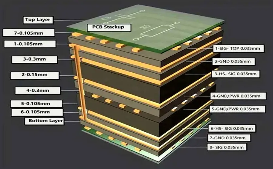
The cost of PCB (Printed Circuit Board) layout is not a fixed value; it's determined by a combination of several interrelated factors. Understanding these key drivers is crucial for effective budgeting and cost management in electronic product development. These primary factors include board complexity, layer count, component density, and routing difficulty.
Board complexity significantly impacts price. A simple single-sided board with few components will cost considerably less than a multi-layer board with high-density components and complex signal routing. The intricacy of the design translates directly into the time and effort required for layout, which affects costs.
The number of layers required for a PCB directly affects the manufacturing complexity and the cost. Single-layer PCBs are the least expensive, followed by double-layer boards and then multi-layer boards, which are necessary for more complex designs. Each layer requires additional processing and materials, driving up costs.
Component density refers to the number of components packed onto a board. Higher component density increases the complexity of the layout and routing process, leading to higher costs. Smaller components with tighter spacing also necessitate more precise placement and routing, further influencing price.
Routing difficulty is another critical factor. Complex signal paths, high-speed signals, and differential pairs demand careful and precise routing to ensure signal integrity. This level of precision requires more time and expertise and therefore increases cost.
| Factor | Impact on Price | Description |
|---|---|---|
| Board Complexity | High | Intricacy of the design (e.g., digital, analog, mixed-signal) |
| Layer Count | Medium to High | Number of conductive layers (single, double, multi-layer) |
| Component Density | Medium to High | Number of components and their proximity on the board |
| Routing Difficulty | Medium to High | Complexity of signal paths (high-speed signals, differential pairs) |

When procuring PCB layout services, understanding the different pricing models is crucial for effective budget management. Two primary models exist: hourly rates and fixed project costs, each with distinct implications for cost predictability and project management.
| Pricing Model | Description | Advantages | Disadvantages | Best Use Case |
|---|---|---|---|---|
| Hourly Rates | Designers charge for each hour spent on the project. | Flexibility to accommodate changes and revisions; potentially lower cost for simple projects. | Uncertainty in final cost; can escalate quickly with scope creep or inefficiencies. | Projects with unclear scope, where changes are highly probable. |
| Fixed Project Costs | A set price is agreed upon before the project begins. | Predictable budget; easier financial planning; cost containment. | Less flexibility for changes; may result in higher costs for unforeseen changes; can be inflexible. | Projects with clear and well-defined specifications. |
Choosing between hourly rates and fixed project costs requires careful consideration of the project’s nature. For projects with well-defined specifications, a fixed price offers budget certainty, while hourly rates are suitable for complex projects where design requirements are likely to change. Always get a detailed estimate, whether it's fixed or hourly, to understand the scope and costs before you start.
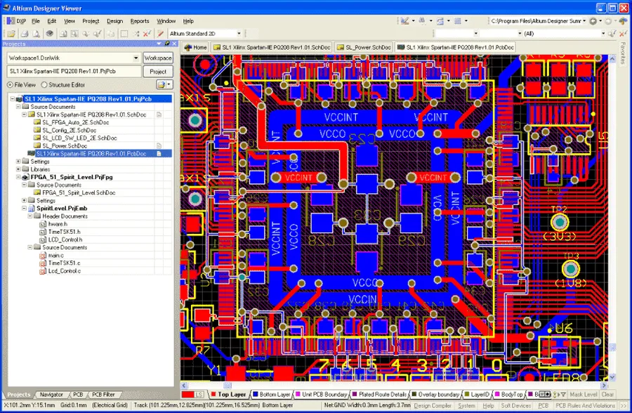
Understanding the typical cost spectrum for PCB layout services is crucial for effective project budgeting. PCB layout prices vary significantly based on the board's complexity, ranging from simple single-layer boards to intricate multi-layer designs with high component density. This section provides a breakdown of these price ranges to help you anticipate costs accurately.
| PCB Complexity | Description | Typical Price Range (USD) | Notes |
|---|---|---|---|
| Simple Single-Layer | Basic boards with components on one side, minimal routing. | $50 - $200 | Suitable for very basic circuits. |
| Standard Double-Layer | Components and traces on both sides, moderate routing. | $150 - $500 | Most common for general purpose electronics. |
| Multi-Layer (4-6 Layers) | Increased layer count for more complex routing and power distribution. | $400 - $1,500 | Suitable for more complex circuitry, higher density designs. |
| Multi-Layer (8+ Layers) | Complex boards with high layer count, dense components, fine-pitch. | $1,200 - $5,000+ | Common in advanced electronics, high-speed applications, and RF circuits. |
| High-Density Interconnect (HDI) | Advanced boards with microvias and blind vias, high pin count devices. | $3,000+ | Typically used in highly advanced electronics where space is at a premium. |
These price ranges are estimates and can be affected by various factors, including the designer's experience, software used, and specific project requirements. For instance, a single-layer board with a simple circuit might fall at the lower end, while a multi-layer board with complex routing and high component density can reach the upper end or even exceed it. The price can also be affected by the turn around time. Expedited turnaround time will increase the price significantly. It's advisable to seek detailed quotes based on your specific needs to get an accurate cost estimate for your PCB layout project. Understanding these ranges, however, will give you a solid starting point when planning the budget for your PCB project.
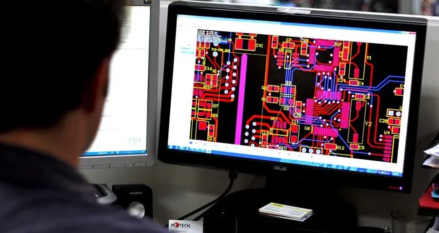
The selection of Electronic Design Automation (EDA) software significantly influences PCB layout pricing. The cost of these tools, along with the specific features they offer, directly affects the overall expense of PCB design projects. Understanding these factors is crucial for cost-effective PCB design.
Different EDA software packages come with varying licensing costs and feature sets. High-end software often includes advanced simulation capabilities and robust design rule checking, but at a premium price. Conversely, more affordable or free options, while sometimes lacking in advanced features, can effectively meet the needs of many projects.
| EDA Software | Licensing Model | Typical Cost Range | Key Features | Suitability |
|---|---|---|---|---|
| Altium Designer | Subscription | $7,000 - $10,000+/year | Advanced Routing, Signal Integrity Analysis, 3D Visualization | Complex, high-performance designs |
| Cadence Allegro | Perpetual/Subscription | $10,000 - $20,000+/year | Advanced Simulation, Large Team Collaboration, High-Speed Design | High-complexity, enterprise projects |
| Mentor Graphics Xpedition | Perpetual/Subscription | $15,000 - $30,000+/year | High-Speed Design, Advanced Simulation, Large Team Collaboration | Very high complexity, enterprise projects |
| PADS Professional | Perpetual/Subscription | $5,000 - $10,000+/year | Mid-range designs, good balance of features and cost | Mid to high complexity projects |
| Eagle (Autodesk) | Subscription | $100 - $500+/year | User-friendly interface, cloud-based, suitable for small teams and startups | Small to medium complexity projects |
| KiCad | Open Source (Free) | $0 | Free and open source with a large user community, good for hobbyist and small projects | Simple to medium complexity projects |
The choice of EDA software should align with project requirements and budget. KiCad, for example, is an excellent choice for budget-conscious projects, while Altium or Cadence might be necessary for highly complex designs with signal integrity requirements. The cost of the software is not the only consideration, the time required for a designer to complete a task with the chosen software should be factored into project cost.

The geographic location of PCB design services significantly impacts pricing due to variations in labor costs, infrastructure, and operational overhead. Understanding these geographical influences is crucial for optimizing your budget when outsourcing PCB layout projects. This section explores the cost differences between North America/Europe and Asia, and discusses strategies to leverage global markets for cost efficiency.
| Region | Typical Hourly Rate for PCB Design | Key Cost Drivers | Overall Cost Implications |
|---|---|---|---|
| North America/Europe | $75 - $150+ | Higher labor costs, advanced infrastructure, higher operating costs. | Generally higher overall PCB layout prices. |
| Asia (e.g., China, India) | $20 - $70 | Lower labor costs, competitive market, established supply chains. | Significantly lower overall PCB layout prices. |
The cost differential arises primarily from discrepancies in labor costs. Regions like North America and Europe, with higher wages and stringent labor regulations, naturally command higher service fees. Conversely, Asian countries, with their larger labor pools and lower living expenses, offer more cost-effective solutions. Furthermore, established manufacturing hubs in Asia benefit from economies of scale and well-developed supply chains, further reducing costs. However, it is essential to consider other factors, including communication, quality control, and intellectual property protection, when deciding to work with an offshore provider.
To optimize costs, you can employ several strategies that leverage global market dynamics. Carefully vet potential partners in different regions based on their experience, certifications, and past projects. Engage in transparent communication to avoid misunderstandings and ensure your requirements are thoroughly understood. Additionally, consider splitting your project by performing the initial design work locally and then send the layout out to an overseas vendor for the detailed layout and manufacturing stages. This hybrid approach helps balance cost efficiency with quality assurance.
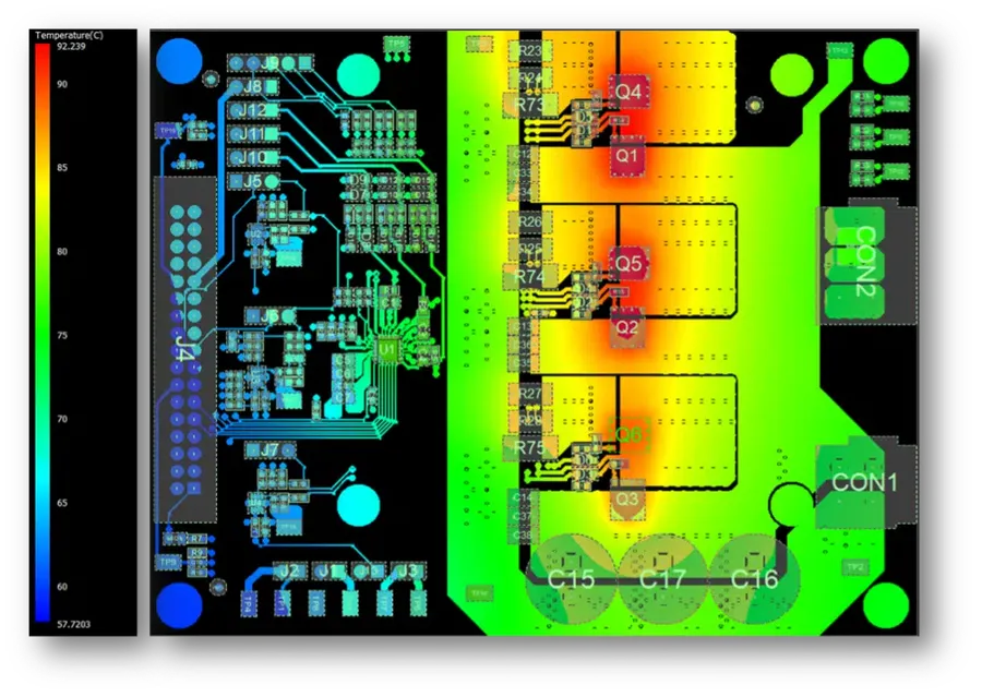
Reducing PCB layout costs without compromising quality requires a strategic approach that focuses on efficient design practices and informed decision-making throughout the design process. By carefully considering various design choices and communication strategies, significant cost savings can be achieved without sacrificing the functional integrity of the PCB.
Understanding the costs associated with PCB layout can be complex, as numerous factors influence the final price. This section addresses common queries regarding PCB layout costs, providing clarity and guidance for those seeking to budget their projects effectively.

The complexity of a Printed Circuit Board (PCB) design significantly impacts its layout cost. This complexity is largely defined by the number of layers, with single-layer, double-layer, and multi-layer boards each presenting unique challenges and corresponding costs. Understanding these differences is crucial for effective budget planning and design optimization.
| PCB Type | Complexity | Typical Cost per Square Inch (USD) | Typical Applications |
|---|---|---|---|
| Single-Layer | Lowest | $0.05 - $0.15 | Simple circuits, basic consumer electronics |
| Double-Layer | Moderate | $0.10 - $0.30 | Intermediate complexity, basic industrial control, IoT |
| Multi-Layer (4-6 Layers) | High | $0.25 - $0.75 | Complex consumer electronics, advanced industrial control, higher power electronics |
| Multi-Layer (8+ Layers) | Very High | $0.60 - $2.00+ | High-speed digital, complex signal processing, high-performance computing |
The cost per square inch is indicative and varies based on other factors like component density and the design house, but clearly demonstrates the escalating cost as PCB complexity increases. Single-layer boards are the simplest and cheapest, suitable for basic applications with straightforward routing requirements. Double-layer boards offer greater routing flexibility, accommodating more complex circuit designs while still being cost-effective for many applications. Multi-layer PCBs, however, are necessary for high-density designs that require routing of many signals, more power or complex signal integrity requirements.
Choosing the right PCB layer configuration involves balancing cost with functionality. A simpler design that uses fewer layers may reduce upfront expenses but could limit the capabilities of the board and increase routing complexity. Conversely, opting for a multi-layer design offers greater flexibility and performance, but at a higher price point. Therefore, careful assessment of application requirements and cost implications is essential before making design decisions. It’s crucial to fully understand the implications of increasing complexity, as it directly translates to higher production and layout design costs. The trade-offs between complexity and budget must be carefully considered at the outset of any PCB design project.
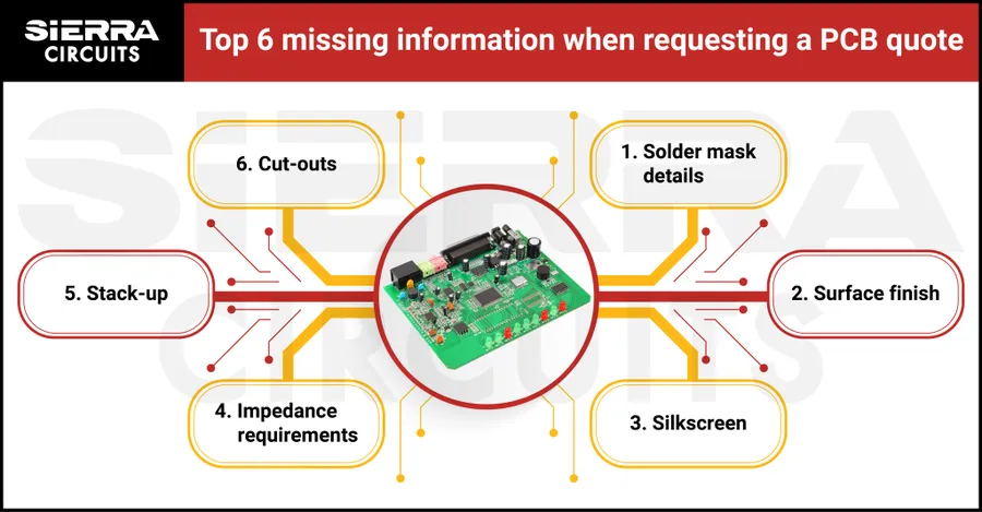
Online PCB layout price calculators can provide preliminary cost estimates, but they should be used with caution. While they offer a quick snapshot of potential costs, accurate quotes require a detailed specification of your project's requirements. Understanding the limitations of these calculators and providing comprehensive information when requesting quotes are crucial steps to obtaining precise pricing.
Here's how to navigate both price calculators and quote requests effectively:
Understanding the various factors that influence PCB layout price is crucial for efficient project management and cost control. The key takeaways include that pcb layout price hinges on complexity, location, design software used, and the chosen pricing model. By adopting the strategies discussed—such as optimizing design for manufacturability, seeking cost-effective global options, and using suitable design software—you can significantly reduce costs while maintaining the desired quality. As technology advances, these insights will remain relevant for ensuring cost-effectiveness in electronic design and production. Always ensure to get detailed quotes and compare the best pcb layout price before committing to your projects to maximize your budget.

