The ubiquitous printed circuit assembly (PCBA) forms the backbone of nearly every electronic device we use today, from our smartphones to complex industrial equipment. This article will take you on an informative journey through PCBA, unraveling its assembly process, key components, quality control measures, and the critical differences between a bare PCB and a fully assembled PCBA. By understanding the fundamentals of PCBA, you gain insight into the technology that powers modern electronics and the precision engineering behind it.
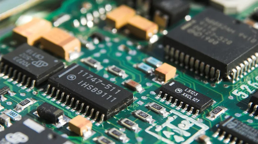
A Printed Circuit Assembly (PCBA) is a fully assembled and functional electronic circuit, created by mounting various electronic components onto a Printed Circuit Board (PCB). This assembly process transforms a bare, non-functional PCB into a complete electronic module, ready for integration into a larger electronic system. PCBA represents the culmination of circuit design and manufacturing.
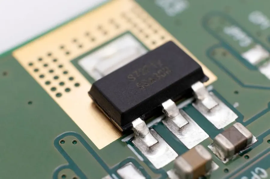
The functionality of a Printed Circuit Assembly (PCBA) hinges on the integration of various electronic components. These components, each with unique characteristics and roles, work in concert to achieve the desired electronic function. Understanding these components is essential to comprehending the overall operation of a PCBA.
| Component Type | Function | Importance | Examples |
|---|---|---|---|
| Resistors | Limit current flow and divide voltage. | Essential for controlling current, setting voltage levels, and preventing damage to sensitive components. | Surface mount resistors (SMD), Axial Lead Resistors |
| Capacitors | Store electrical energy and filter out unwanted noise or voltage fluctuations. | Crucial for power supply smoothing, signal filtering, and timing applications. | Ceramic capacitors, electrolytic capacitors, tantalum capacitors |
| Inductors | Store energy in a magnetic field, filter out high frequency noise and block AC signals. | Used in power electronics, signal filtering, and electromagnetic interference suppression. | Ferrite core inductors, air core inductors |
| Diodes | Allow current to flow in one direction, rectify AC signals to DC, and protect against over voltage. | Critical for rectifying AC power, signal routing, and overvoltage protection. | Schottky diodes, Zener diodes, Light-Emitting Diodes (LEDs) |
| Transistors | Amplify or switch electronic signals and electrical power. | Fundamental building blocks of modern electronics, used in amplifiers, switches, and logic circuits. | Bipolar Junction Transistors (BJTs), Field-Effect Transistors (FETs) |
| Integrated Circuits (ICs) | Perform complex functions on a single chip, such as processing data or controlling operations. | Core elements of sophisticated electronic systems. Enable complex functionalities in a single small device | Microcontrollers (MCUs), Microprocessors (MPUs), Operational Amplifiers (Op-Amps) |
| Connectors | Provide connection points between different parts of the circuit or external devices. | Facilitate signal transmission and power delivery between different parts of a PCBA or to the external environment. | Headers, terminals, USB connectors, Ethernet connectors |
| Crystals/Oscillators | Provide accurate timing signals for digital circuits. | Essential for synchronized operation of microprocessors and other time-sensitive components. | Quartz crystals, Crystal Oscillators |
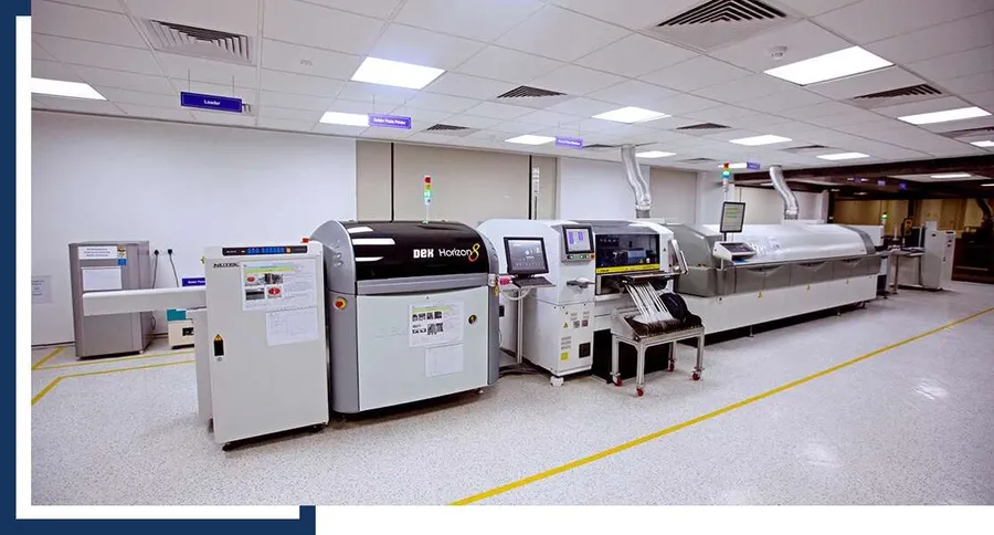
The printed circuit board assembly (PCBA) manufacturing process is a complex and multi-staged operation that transforms a bare PCB into a fully functional electronic module. This process involves precise application of solder, accurate placement of electronic components, and rigorous quality control measures to ensure the reliability and performance of the final product.
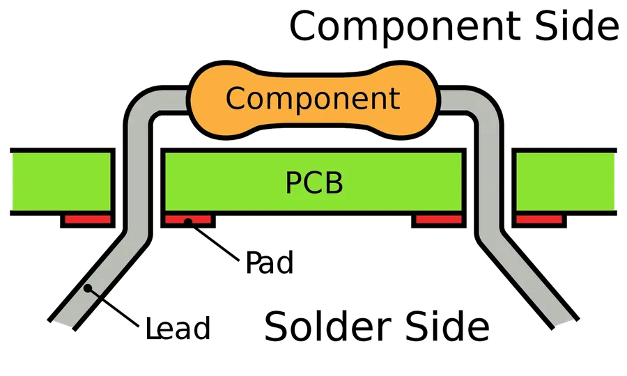
Printed Circuit Board Assembly (PCBA) utilizes two primary methods for mounting electronic components: Surface Mount Technology (SMT) and Through-Hole Technology (THT). Each method possesses unique characteristics, advantages, and limitations that dictate their application in various electronic devices.
| Feature | Surface Mount Technology (SMT) | Through-Hole Technology (THT) |
|---|---|---|
| Component Mounting | Components are mounted directly onto the surface of the PCB. | Components have leads that are inserted through holes in the PCB. |
| Component Size | Typically smaller and more compact components. | Typically larger components with leads. |
| Assembly Process | Automated process with pick-and-place machines and reflow soldering. | Can be manual or automated, often requiring wave soldering. |
| Density | Higher component density possible, leading to smaller PCBs. | Lower component density due to larger component sizes and leads. |
| Cost | Generally lower assembly cost for mass production. | Higher assembly cost, especially for manual assembly |
| Reliability | Good reliability for most applications, but solder joints can be more susceptible to mechanical stress. | Stronger mechanical bond with the PCB, more resistant to mechanical stress. |
| Applications | Widely used in most modern electronics, including consumer electronics. | Common in applications requiring robust connections and high power handling. |
| Repair | More challenging to repair due to component size and mounting | Easier to repair and replace components. |
The choice between SMT and THT depends on various factors, including the size and complexity of the PCB, the required density of components, the cost constraints, and the desired level of mechanical robustness. While SMT is dominant in modern electronics due to its efficiency and suitability for mass production, THT remains relevant for specific applications where its robustness is essential. A hybrid approach combining both technologies is often employed to optimize performance and cost in complex PCBA.
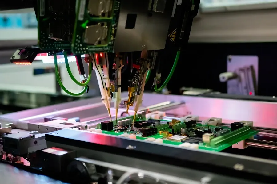
Rigorous quality control and testing are paramount in PCBA manufacturing to ensure reliability and functionality. These processes involve a multi-stage approach, starting from visual inspection to advanced techniques like X-ray and functional testing, to identify and rectify any defects that may compromise the final product.
| Inspection Method | Description | Purpose | Technology |
|---|---|---|---|
| Visual Inspection | Manual inspection of the PCBA by trained personnel. | Detects obvious defects such as missing components, misaligned parts, solder bridges, and damaged components. | Human observation, magnifying glass, microscopes |
| Automated Optical Inspection (AOI) | Automated inspection using cameras and light sources. | Identifies defects such as solder joint issues, component placement errors, and incorrect component polarity, improving inspection speed and consistency compared to visual inspection. | High-resolution cameras, LED lighting, image processing algorithms. |
| X-ray Inspection | Uses X-rays to inspect solder joints and internal structures. | Examines solder joints hidden under components, detects solder voids, and internal component damage. Ensures connections and solder integrity, crucial for Ball Grid Array (BGA) packages. | X-ray source and detector system. |
| Functional Testing | Tests the PCBA under operational conditions. | Validates that the PCBA performs as designed, according to its functional specification, by simulating its use-case. | Test fixtures, power supplies, measuring instruments, dedicated test software |
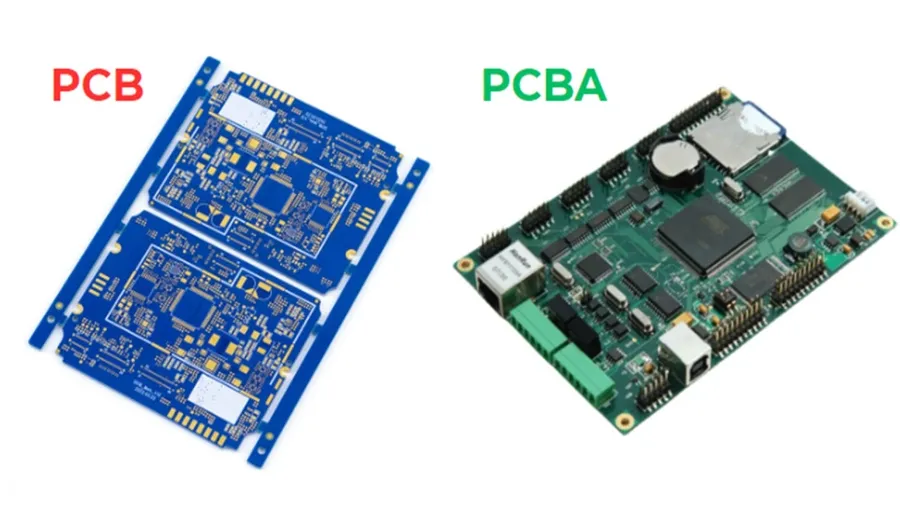
The terms PCB (Printed Circuit Board) and PCBA (Printed Circuit Board Assembly) are often used in the electronics industry, but they represent distinct stages in the creation of a functional electronic device. A PCB is the foundational base, a substrate with conductive pathways, while a PCBA is the fully assembled, functional board, ready to be integrated into a product.
| Feature | PCB | PCBA |
|---|---|---|
| Definition | Bare board with conductive tracks, pads, and vias | PCB with all electronic components soldered on |
| Functionality | Provides electrical connections | Functional electronic module |
| Components | None | Resistors, capacitors, ICs, etc. |
| State | Unpopulated | Populated |
| Application | Base for electronic assembly | Ready for integration into devices |
| Testing | Basic continuity and isolation tests | Functional tests |
| Cost | Lower cost than PCBA | Higher cost due to component and assembly costs |
In essence, a PCB is the blueprint upon which a PCBA is built. The distinction is crucial because while PCBs undergo basic electrical testing to confirm connectivity and isolation, PCBAs are subject to comprehensive functional testing to ensure that all the components work together as intended. The transition from PCB to PCBA signifies the shift from a passive element to an active one, capable of carrying out specified electronic operations.
This section addresses common inquiries about Printed Circuit Board Assemblies (PCBAs), providing clear and concise answers to help clarify any confusion surrounding these critical electronic components.
The cost of Printed Circuit Board Assembly (PCBA) is influenced by a multitude of factors, requiring a holistic understanding to manage expenses effectively. These factors can be broadly categorized into component-related costs, production-related costs, and material costs. A thorough understanding of these influencing parameters enables cost-effective design and procurement strategies, crucial for efficient product development and market competitiveness.
| Cost Factor | Description | Impact on Cost |
|---|---|---|
| Component Complexity | The intricacy and type of components (e.g., integrated circuits, microcontrollers, passives) | Higher complexity and specialized components increase cost due to design, sourcing, and placement requirements. |
| Production Volume | The quantity of PCBA units being manufactured in a production run. | Larger volumes typically lower per-unit cost through economies of scale, while smaller volumes incur higher setup and overhead costs. |
| PCB Material | The material used to fabricate the base PCB (e.g., FR-4, flexible substrates, high-frequency laminates). | Specialized materials, such as those used for high-frequency applications or thermal management, elevate PCB costs. |
| Labor Costs | Expenses associated with personnel involved in the PCBA process, including design, assembly, testing, and inspection. | Higher labor rates, especially for skilled technicians and engineers, increase overall PCBA costs. |
| Assembly Technology | The specific assembly methods employed, such as Surface Mount Technology (SMT), through-hole, or mixed technologies. | Advanced assembly techniques, like SMT for fine-pitch components, require specialized equipment and processes, influencing costs. |
| Testing and Quality Control | The level of testing and inspection procedures applied during the assembly process (e.g., functional testing, AOI, X-ray inspection). | Rigorous testing and inspection increase reliability but also add to the overall cost, balancing quality with budget constraints. |
| Lead Time | The timeframe required to complete the PCBA process, from design to delivery. | Short lead times often incur premium costs, while extended lead times may offer cost savings through streamlined processes. |
The printed circuit assembly (PCBA) industry is continuously evolving, driven by demands for increased functionality, higher performance, and smaller form factors. Several emerging trends are shaping the future of PCBA, encompassing advancements in materials, technologies, and manufacturing processes. These advancements aim to address the challenges of modern electronics manufacturing and push the boundaries of what is achievable.
In conclusion, printed circuit assembly (PCBA) is a pivotal aspect of electronics manufacturing. Understanding its process, key components, and quality control is vital. The difference between a bare PCB and the completed PCBA is significant, highlighting the transition from a blank board to a fully functional electronic module. As technology continues to advance, so too will the methods and techniques used in PCBA, ensuring a key role in shaping the electronics of tomorrow.

