In our increasingly digital world, printed circuit boards (PCBs) are the unsung heroes enabling the functionality of almost every electronic device we use daily. From smartphones and computers to medical equipment and industrial machinery, these intricate boards are the foundation upon which modern technology is built. This article explores the core concepts of PCBs, guiding you through their definition, composition, design, and real-world applications, offering a solid understanding of this critical component in the realm of electronics.
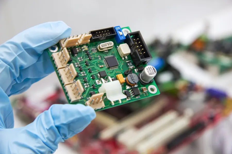
A Printed Circuit Board (PCB) serves as the foundational platform for electronic components, providing both the necessary mechanical support and the intricate electrical connections required for a functional electronic device. Essentially, it's the 'backbone' of nearly every modern electronic device, ensuring components are correctly interconnected to perform their designated tasks.
The basic structure of a PCB comprises a substrate material, which is typically a non-conductive base, and conductive pathways, generally made of copper, that form the electrical circuit. The substrate provides the mechanical structure, while the copper traces etched onto it enable the flow of electrical signals between components.
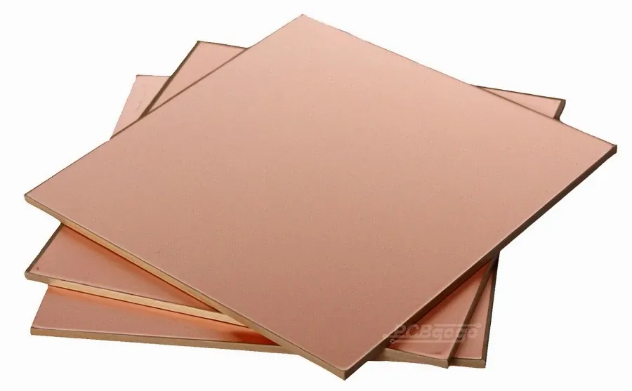
The performance and reliability of a printed circuit board (PCB) are significantly influenced by the materials used in its fabrication. These materials provide the necessary mechanical support, electrical insulation, and conductive pathways for electronic components to function correctly. The selection of these materials is critical and depends on the intended application, operating environment, and cost considerations.
| Material | Description | Key Properties | Typical Applications |
|---|---|---|---|
| FR-4 | A composite material made from woven fiberglass cloth with an epoxy resin binder. | Good electrical insulation, high strength-to-weight ratio, flame retardant, cost-effective. | Most general purpose PCBs, common in consumer electronics and industrial applications. |
| Metal Core (Aluminum/Copper) | Metal substrate with a dielectric layer and copper circuitry. | Excellent thermal conductivity, good mechanical strength. | LED lighting, power electronics, applications requiring efficient heat dissipation. |
| Rigid-Flex Materials | Combination of rigid and flexible materials, typically polyimide or polyester based. | High flexibility, can withstand repeated bending, high-density interconnections. | Aerospace, medical devices, portable electronics, applications that require complex 3D shapes. |
| High-Frequency Laminates (e.g., PTFE) | Laminates with low dielectric constant and loss tangent, commonly Polytetrafluoroethylene (PTFE) based. | Excellent signal integrity, low loss at high frequencies, stable performance over temperature. | RF circuits, microwave communication, high-speed digital applications. |
Beyond the substrate, copper is the most common conductive material used to create traces and pads on a PCB. It is preferred for its excellent conductivity and relatively low cost. Other conductive materials, such as gold or nickel, are sometimes used for plating to enhance the conductivity, solderability, and corrosion resistance of the copper.
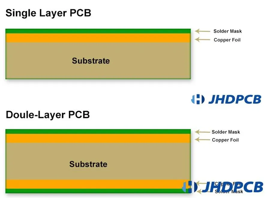
Printed circuit boards (PCBs) are categorized based on their layer count, construction, and specific application needs. The choice of PCB type significantly impacts the functionality, cost, and complexity of electronic devices.
| PCB Type | Description | Applications | Advantages | Disadvantages |
|---|---|---|---|---|
| Single-Layer PCB | Contains conductive material on only one side of the substrate. | Simple electronics, basic circuits, lighting, low-cost devices. | Low cost, easy to manufacture, suitable for simple designs. | Limited component density, not suitable for complex circuits. |
| Double-Layer PCB | Has conductive material on both sides of the substrate. | Power supplies, basic audio circuits, industrial control, most common type. | Higher circuit density than single-layer, more complex circuits possible. | Still limited in density compared to multilayer, less effective with high speed signals. |
| Multilayer PCB | Features three or more layers of conductive material within the board. | High-end computers, servers, advanced medical equipment, complex signal processing. | Very high density, capable of complex designs, excellent signal integrity. | Expensive, complex to manufacture, longer lead times. |
| Flexible PCB | Constructed on a flexible substrate, allowing it to bend and flex. | Wearable devices, automotive applications, printers, camera lens systems. | Flexible, lightweight, can fit into tight spaces, vibration resistance. | More expensive than rigid boards, potential for tearing or damage. |
| Rigid-Flex PCB | Combines flexible circuits with rigid board sections. | Aerospace, military, medical equipment, high-end electronics. | Combines advantages of both rigid and flex boards, enhanced reliability. | Complex to design and manufacture, higher cost than rigid or flexible PCBs alone. |
| HDI PCB | High-Density Interconnect PCB featuring very fine lines and vias. | Smartphones, tablets, high-performance computing, complex integrated circuits. | Extremely high density, suitable for miniaturized devices, better signal integrity. | More expensive, requires specialized manufacturing processes. |
| Metal Core PCB | Features a metal core (typically aluminum or copper) for heat dissipation. | LED lighting, power electronics, high power equipment, high temperature applications. | Excellent thermal management, good mechanical stability. | Can be heavier, potentially more expensive, different manufacturing needs. |
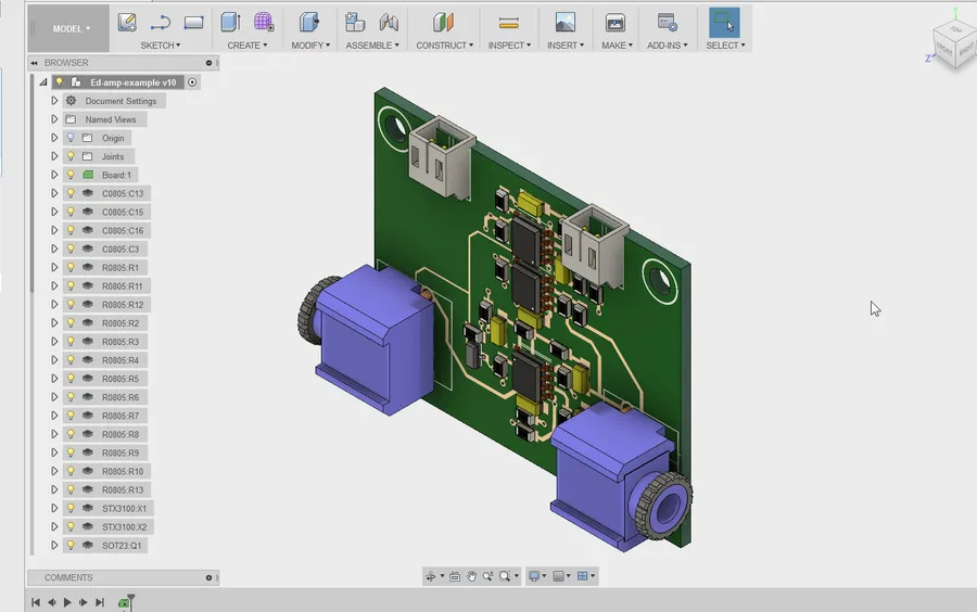
The design of a printed circuit board (PCB) is a multi-stage process that transforms an abstract electronic circuit into a physical reality. It involves converting a schematic diagram into a functional board layout using Electronic Design Automation (EDA) tools, requiring meticulous attention to electrical, thermal, and mechanical aspects.
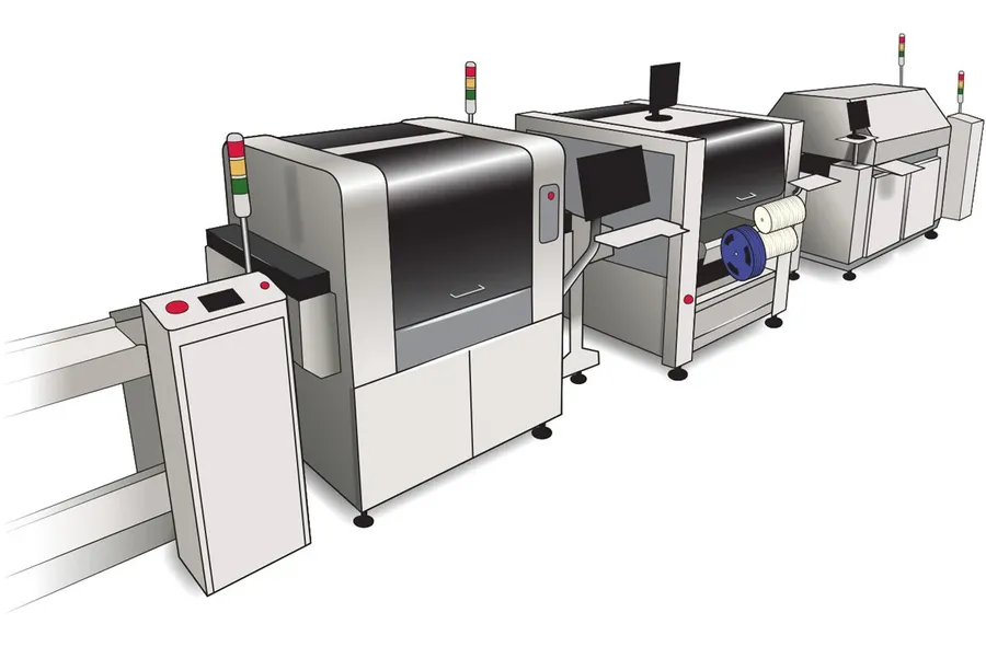
The fabrication of printed circuit boards (PCBs) is a complex, multi-stage process that transforms a digital design into a physical substrate that provides both mechanical support and electrical connections for electronic components. This process includes creating conductive pathways, known as traces, and pads for component attachment, as well as drilling holes for component leads and vias, and applying a solder mask and silkscreen for protection and identification.
The PCB manufacturing process can vary depending on the type of board being produced, the complexity of the design, and the volume of production. However, the core steps remain consistent across most manufacturing methods. Below, we delve into the various stages and highlight the advantages and disadvantages of different approaches.
| Manufacturing Step | Description | Methods | Advantages | Disadvantages |
|---|---|---|---|---|
| Material Preparation | Cutting the base material (e.g., FR-4) into the required panel sizes. | Shearing, Sawing | Precise cutting, fast | May create rough edges if not careful |
| Inner Layer Imaging | Transferring the circuit pattern to copper clad laminate using a photo-imaging process. | Photolithography | High precision | Multi-stage process |
| Etching | Removing the unwanted copper, leaving only the conductive traces and pads. | Chemical etching | Efficient for large-scale production | Requires careful handling of chemicals |
| Layer Alignment and Lamination | Stacking the etched layers with prepreg (an adhesive layer) and pressing under heat and pressure to create the multilayer PCB. | Hydraulic Press Lamination | Ensures strong layer adhesion | Can be time-consuming for thick boards |
| Drilling | Creating holes for component leads, vias (interlayer connections), and mounting. | CNC drilling, Laser drilling | High precision drilling, automation | Requires specialized equipment |
| Plating | Applying copper, and other metals to the inner walls of the drilled holes to establish electrical connection between layers. | Electrolytic Plating | Good electrical conductivity | Can be costly |
| Outer Layer Imaging and Etching | Transferring the final circuit pattern to the outer layer using photo-imaging and etching. | Photolithography | High resolution pattern transfer | Needs specific chemicals |
| Solder Mask Application | Applying a solder mask to protect the traces and pads from oxidation and prevent solder bridging during assembly. | Screen printing, photo-imaging | Protects board from damage | Needs precise alignment |
| Silkscreen Printing | Printing component labels, logos, and other identifiers on the PCB surface. | Screen printing, inkjet printing | Good visibility, cost-effective | Limited resolution |
| Surface Finish | Applying a protective finish to the exposed copper to prevent oxidation, improve solderability, and protect the material. | ENIG, HASL, Immersion Silver, OSP | Good solderability and protection | Each has different characteristics in cost, protection, and processing. |
| Electrical Test | Testing the PCB to ensure the electrical connections are accurate and functional using in-circuit testing or flying probe testing. | Automated Optical Inspection (AOI), in-circuit testing (ICT) | Identifies manufacturing defects | Expensive equipment |
| Profiling and Separation | Cutting individual PCBs from the panel. | Routing, v-scoring | Provides dimensionally accurate board | May introduce stress |
The choice of manufacturing methods depends on factors such as the quantity needed, cost constraints, and design complexity. For example, high-volume production often uses automated processes, while low-volume prototyping may employ more manual techniques. Choosing the right method can optimize both the quality and the cost-effectiveness of PCB production.
This section addresses common questions regarding printed circuit boards (PCBs), providing clear and concise answers to enhance understanding of their function, limitations, and applications. We aim to clarify frequently encountered queries, drawing on established engineering principles and industry best practices.
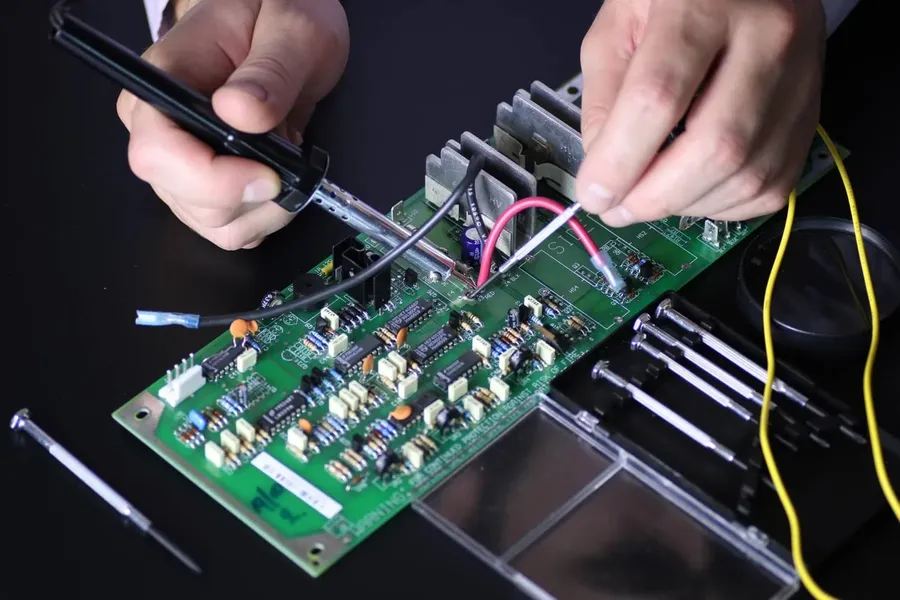
Printed circuit boards (PCBs) are the ubiquitous foundation of modern electronics, facilitating connections and mechanical support for electronic components across a diverse range of applications. Their adaptability and reliability make them indispensable in virtually every industry that utilizes electronic technology.
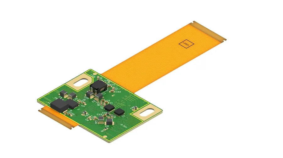
The printed circuit board (PCB) industry is in a state of constant evolution, driven by the increasing demands for smaller, faster, and more efficient electronic devices. This section explores the key trends shaping the future of PCB technology, encompassing advancements in materials, design, and manufacturing processes.
Printed circuit boards are pivotal to modern electronics, forming the core of almost every device we use. From understanding their material composition and design process to exploring varied applications and future trends, this guide offers a comprehensive overview of PCBs. The continuous innovation in PCB technology will drive forward technological progress, highlighting the importance of this foundational component in the evolution of electronics.

